


Serviços Personalizados
Journal
Artigo
 Inglês (pdf)
 Artigo em XML
 Referências do artigo
 Enviar este artigo por email
Indicadores
-
 Citado por SciELO
 -
 Acessos
Links relacionados
-
 Similares em
SciELO
Similares em
SciELO
Compartilhar

 Permalink
Superficies y vacío
versão impressa ISSN 1665-3521
Superf. vacío vol.26 no.4 Ciudad de México Dez. 2013
Electronic transitions in single and double quantum wells made of III-V compound semiconductors
Velásquez-Arriaga A., Hernández-Rosas J. *, Ponce H., López-López M.**
*UPIITA-IPN Av. IPN 2580, México D.F. 07340, México. jhr@fis.cinvestav.mx
**Departamento de Física, Centro de Investigación y Estudios Avanzados del IPN Apartado Postal 14-740, México D.F., México 07360.
Recibido: 21 de agosto de 2013.
Aceptado: 15 de noviembre de 2013.
Abstract
In this work, we calculate the electronic inter-band transitions in low dimensional nanostructures employing the effective mass approximation. With the help of the well-known models of square quantum well (SQW) and the symmetric square double quantum well (DQW), we calculate the energy levels in nanostructures commonly grown by molecular beam epitaxy (MBE) of III-V compound semiconductors. We choose in our calculations quantum wells (QWs) made of heterostructures without strain such as GaAs/AlxGa1-xAs, as well as heterostructures where the strain is very important such as InxGa1-xAs/GaAs and InAs/GaAs. We present our results showing the electronic transition energy versus the well width in the SQW case, or versus the middle barrier width in the DQW case. A discussion about the wave functions in the SQW and its coupling in the DQW is included.
Keywords: Quantum well; Double quantum well; Compound semiconductor; MBE; Heterostructure; Wavefuntion
1. Introduction
The textbook problems of quantum mechanics related to the single and the double square quantum well (QW), have at present relevant importance because the research in low dimensional semiconductor heterostructures is not exhausted [1-3]. By means of heteroepitaxy techniques such as MBE, the growth of QWs with a few monoatomic layers or even with a sub-monolayer thickness is a routine fact [4]. The optical properties of QWs are strongly dependent on the structure dimensions, i.e. the quantum confinement is an important property for these nanostructures. The strain originated by the lattice mismatch between neighbor heterostructure layers, is another profitable property in QWs. The InxGa1-xAs/GaAs system shows a strain at the interfaces as a function of the In concentration. The maximum strain is obtained for the InAs/GaAs system with a mismatch of ~7%. As a consequence, it is not possible to deposit many layers of InAs on GaAs substrates in a coherent growth, forming the so-called 8-layer. In fact, the critical thickness is about 1.7 monolayers, after this thickness the lattice is relaxed first by producing self-assembled nano-islands which can be used as quantum dots (SAQDs) [5,6]. The SAQDs suffer a redshift in the photoluminescence (PL) peak with respect to the very thin epitaxial layer before the emerging of three-dimensional (3D) structures. This kind of nanostructures is object of intense study at present due to its complexity [7].
The matter of coupling two SQWs forming a DQW has been used to figure out several physics problems, for instance to study the transport and lifetime of carriers in heterostructures [8]. As well as, with this system, it has been determined the band offset at the highly strained InAs/GaAs interface [9]. The DQW system also is quite interesting in theoretical studies in quantum coherence and interference phenomena [10].
Due to several reasons, such as defects at interfaces, segregation of chemical species, et cetera; real QWs not always have perfect abrupt interfaces, a more complicated well profile at the interfaces could be solved by the transfer matrix method [11]. In this work, we calculate the electronic transitions of ideal SQWs and symmetric DQWs with abrupt interfaces as a function of its width. We studied the unstrained and strained heterostructures made of GaAs/AlxGa1-xAs and InxGa1-xAs/GaAs, respectively. Including the highly strained case for the InAs/GaAs system [4,5]. We performed the calculations only along the conventional [100]-oriented substrates due to the fact in other growth directions corrugated surfaces can appear, forming self-assembled quantum wires (SAQWRs) and, where the model of the SQW could not match well with the experiment [12]. Electronic transitions are also temperature dependent, so we considered such effects in the band-gap energy. We finally study the wave functions in order to obtain further information on the physics of these systems.
2. Theory
Theoretical calculations about QWs heterostructures in the effective mass approximation have been presented by Bastard [13]. If mW is the effective mass of the charge carrier in a well, and mB the effective mass in the barrier; the respective even and odd bound states energies E in a SWQ of width 2a and depth V0 are given by solving the transcendental equations
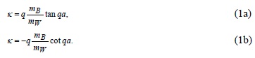
where q and k are the wave-vector in the well and the barrier, respectively. These quantities are defined as k2 =-2mB|E|/h2 and q2=2mW(V0-|E|)/h2.
Likewise, following similar calculations to the SQW, it can be found out the bound state energies of two identical coupled SQWs of width a separated by a barrier of width b, i.e. the symmetric DQW. The energy level degeneracy of the two identical SQWs is lifted when the SQWs approach together, emerging the symmetric and antisymmetric states of the DQW [3], being the first symmetric state the ground state. If the middle barrier is made of the same material to the barriers surrounding the coupled wells, the eigenenergies are given by solving the next transcendental equations
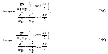
where Eq. (2a) corresponds to the symmetric energy levels, and Eq. (2b) corresponds to the antisymmetric energy levels. Being q and k the same wavevectors as in the SQW case. For a well width fixed a, there are two important limits in theses equations. The first one is when the barrier width b tends to zero. Thus, equations (2a) and (2b) tend to equations (1a) and (1b), respectively. One consequence of this limit is that the first antisymmetric energy level in the DQW not always exists as occurs with the odd energy level in the SQW. The second limit is when b tends to infinite, thus the eigenvalues in Eq. (2a) become the same as the Eq. (2b). The way we have presented equations (2a) and (2b), i. e. the eigen-value conditions of the DQW, is a generalization of the solutions given by Gasiorowicz for the DQW, where we have taken into account the effective masses of the charge carriers in each layer [14].
Without taking into account the exciton, in semiconductors with direct band gap at the r point, the electronic interband transition energy Eg,eff(T) for a given temperature is given by Eg,eff(T)= Eg(T)+Eme+Enhh. Being Eg(T) the temperature dependent bulk band gap width of the well layer. Whereas Eme and Enhh are the energies of the m-th subband of electrons and the n-th subband heavy holes in the QWs. In order to obtain the temperature dependence of the band-gap energy we used the Varshni's formula [15]:
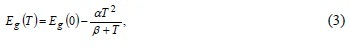
where Eg(0) is the energy gap at 0 K, α and β are the fitting parameters of the material.
In strained QWs, the band gap experiments a shift AE corresponding to the strain for mismatched interfaces. Therefore, we should add also this term to the energy Eg,eff(T). For the [100] direction, the energy shift is given by
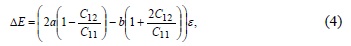
where C11 and C12 are the elastic constants, ε the strain; and, a and b the deformation potentials [16].
3. Results and Discussions
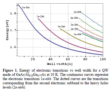
It is well established that the electronic transitions observed in photoluminescence (PL) and photoluminescence excitation (PLE) techniques are those with the same parity. However, we present our results showing all the interband transitions no matter if they were or not possible to be observed. In such a case, the width where one possible transition begins is the same where a new level in one of the wells is emerging. Figure 1 shows electronic transitions in a SQW at 10 K for the GaAs/Al0.23Ga0.77As system. The parameters we used in the Varnish's formula for GaAs are α = 5.4x10⁻⁴ eV/K, β= 200 K and Eg(0)= 1.5192 eV. On the other hand, for Al0.23Ga0.77As the band gap is 1.963 eV at the same temperature. In GaAs, the effective masses are 0.0665m0 and 0.51m0, for the electrons and the heavy holes; respectively, where m0 is the free electron mass [17]. The remaining parameters of Al0.23Ga0.77As were taken from the same reference. For our calculation we employed the conduction band offset ratio at the GaAs/Al0.23Ga0.77As interface as Qc = 0.65 [18]. Figure 1 shows only one electronic transition (1e-1 hh) up to the emerging of the second level n = 2 at the heavy holes band at the well width 2a = 26 Å. With the increasing of the well width the energy spectrum is enriched with a variety of transitions. The well width broadening also causes that the energy of the electronic transition 1e-1 hh approaches to the gap of the well, that in the case of GaAs at 10 K is Eg(10)= 1.5189 eV.
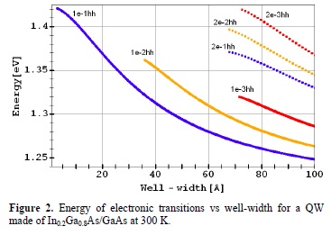
For the InxGa1-xAs/GaAs system with x = 0.2, a biaxial compressive stress is applied to the well layer. Thus, the lattice mismatch of about 1.4% among In0.2Ga0.8As and the barrier layers increases the unstrained band gap by an energy shift of 72.4 meV at 300 K. Therefore, for this system, the bulk band gap Eg(300) = 1.140 eV goes up to 1.212 eV [19]. In this case, the conduction band offset ratio of Qc = 0.71 was used [18]. Figure 2 shows the energy transitions for an In0.2Ga0.8As SQW at 300 K as a function of well width. The behavior of the electronic interband transitions is similar to the shown for Al0.23Ga0.77As. However, in figure 2 we do not observe the transitions 1e-4hh, 2e-4hh, etc. because of the fourth heavy hole level emerges up a to a well thickness of 107 Å.
Normalized wave functions for the electrons and heavy holes associated with two In0.2Ga0.8As/GaAs QWs of 30 and 50 Å well width are shown in figure 3. The calculations display a greater percentage of localization inside the QW for the heavy holes than for the electrons in the ground state. The electronic wave function in the wider QW has 76 % of probability to localize the electron inside the well, whereas there is a 53 % of probability to localize the electron inside the QW of 30 Å. With respect to the heavy holes, there is a 92 % of probability to find the heavy hole in the wider QW versus 79 % in the thinner QW. For the odd state, the probability of the heavy holes to be localized inside the 50 Å QW decreases to 58 %.
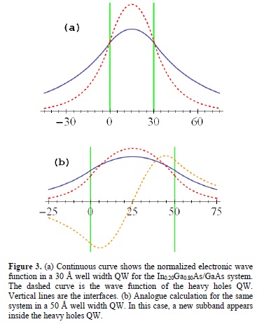
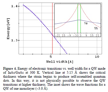
Figure 4 shows the transition energy as a function of well width for InAs/GaAs SQW. In this calculations, we have used the conduction band offset ratio of Qc = 0.58 [9]. Theoretically there is not limit in the well width. However, it is important to note that the Stranski-Krastanov mechanism stops the possibility to growth SQWs of InAs/GaAs with arbitrary well width. Thus, the InAs/GaAs quantum wells support only one level in the conduction band as well as in the valence band, allowing only the ground state transition. About the energy shift in the bulk band gap in the InAs monolayer, the Eq. (4) gives 103 meV at 300 K. Therefore, the bulk band gap of InAs increases from 0.350 to 0.453 eV. Our calculations in InAs monolayers are in very good agreement with reported PL experiments [4], but also without the use of delta functions frequently used to represent these very thin layers [9]. In the case of one nominal monolayer of InAs embedded in barriers of GaAs, the calculation shows a 4.25 % of probability for electrons to be confined, versus 20 % for heavy holes.
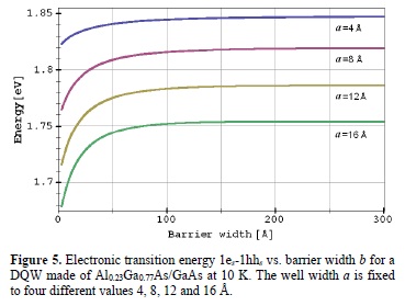
Electronic transition energies corresponding to the ground state of the electrons and holes of a DQW for the system GaAs/Al0.23Ga0.77As at 10 K are shown in figure 5. In this figure, the calculations were done fixing the well width a to four different values 4, 8, 12 and 16 Å. From the 1es-1hhs transition energies versus the barrier width we can observe two limits. For the first limit, when the barrier width b tends to zero, the transition energy tends to the corresponding SQW of width 2a, due to the total coupling of both SQWs when the barrier disappears. In the second limit, we can see as the barrier width increases, the transition energy tends to a constant value, which corresponds to two decoupled SQWs of the same width a. Thus, the transition energies at the barrier widths b=0 Å and b=300 Å in figure 5 have corresponding values with the electronic transition 1e-1 hh showed in the figure 1.
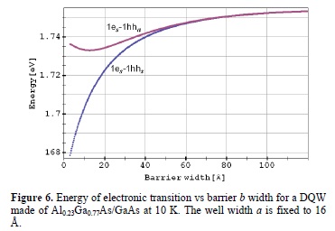
The 1es-1hhs transition shown in figure 5 corresponding to α= 16 Å is compared with the 1es-1hhα transition in figure 6. We can see as the barrier width b increases, both transitions converge very fast. This result is in agreement with the behaviour of the equations (2) when b tends to infinite. We stated in Eq. (2b) that not always exists the antisymmetric states. Thus, at a = 16 Å and b = 3 Å, there are already the first two states in the hole's DQW, but only one in the electron's DQW. Figure 6 took into account this consideration.The analysis of the wave functions in a DQW is given in figure 7. The system under study is again Al0.23Ga0.77As/GaAs at 10 K. Figure 7a shows a DQW with parameters a=6 Å and b=3 Å. Similarly to the SQW case, the calculations also show a greater percentage of localization inside the wells for the heavy holes than for the electrons in the ground state. The electronic wave function has 5.87 % of probability to localize the electron inside each well, whereas there is a 13.9 % of probability to localize the heavy hole inside their corresponding wells. About the probability to localize the charge carriers in the middle barrier, there is a probability of 0.00016 % for the electrons versus 0.0026 % for the heavy holes. These data contrast with the great probability to localize the charge carriers in the external barriers: 44.13 % for the electrons versus 36.1 % for the heavy holes. Figure 7b shows a DQW with parameters a=50 Å and b=100 Å. The wells are weakly coupled; however the probability of tunneling between the wells is greater than the DQW shown in figure 7a. In the middle barrier, there is a probability of 0.25 % to find the electrons versus 0.07 % for the heavy holes. We also have a probability of finding the electrons in each well of 39.82 % and a probability of 47.28 % for the heavy holes. Meanwhile, the probability of finding the electrons is 10.05 % at the external barriers versus 2.68 % for the heavy holes. With respect to the antisymmetric state located at the heavy holes we have an increased probability to find them in the middle barrier, being of 13 %. At the same time, reducing the probability at the external barriers to 1.4 %. Finally, the probability at each well is 42.1 %.
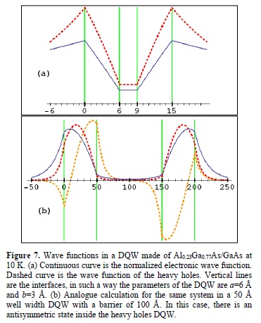
We can see from the figure 7b, that although there is a little probability to find the charge carrier in the middle barrier; the wells are strongly coupled even separated at 100 Å, in such a way the wave functions are still quite different from two decoupled SQWs as we can see in figure 3. The differences in probabilities of finding the charge carriers in each one of the regions in SQWs and the DQWs, are in all cases mainly due to the differences in their effective masses, but also in the differences of the band offset of the wells.
4. Conclusions
In a QW heterostructure there is always at least one electronic transition, this is the case of the very thin delta-layers heterostructures made of InAs/GaAs. In QWs with or without strain, as the well-width increases, the system begins to have a richer subband structure. At thinner QWs the charge carriers have a higher probability to be localized at the barriers. The coupling between SQWs can be studied qualitatively by means of the shape of the wave function, and quantitatively by the probabilities of finding the charge carriers. In identical coupled QWs, the degeneracy splits in antisymmetric and symmetric energy level. Becoming the last one in the ground state. The energetic separation between levels or transitions can also give us quantitative information about the degree of coupling between SQWs forming a DQW.
Acknowledgments
The authors are thankful to SIP-IPN project No 20131035, the Mexican Agencies CONACYT-SENER project No 151076, and ICyT-DF, for financial support.
The authors also thank the technical assistance of E. Gómez.
[1] I. Dhifallah, M. Daoudi, A. Bardaoui, B. Eljani, A. Ouerghi, R. Chtourou, J. Lumines. 131, 1007 (2011). [ Links ]
[2] A. Castañeda-Medina and R.M. Gutiérrez, Phys. Status Solidi B. 248, 2877 (2011). [ Links ]
[3] A. Acus and A. Dargys, Phys. Scr. 84, 015703 (2011). [ Links ]
[4] J. Hernández-Rosas, J.G. Mendoza-Álvarez, S. Gallardo- Hernández, E. Cruz-Hernández, J.S. Rojas-Ramírez, and M. López-López, Microelectron. J. 39, 1284 (2008). [ Links ]
[5] W. Rudno-Rudziński, G. Sek, and J. Misiewicz, T. E. Lamas, A. A. Quivy, J. Appl. Phys. 101, 073518 (2007). [ Links ]
[6] H. Morales-Cortés, C. Mejía-García, V.H. Méndez-García, D. Vázquez-Cortés, J.S. Rojas-Ramírez, R. Contreras-Guerrero, M. Ramírez-López, I. Martínez-Velis and M López-López, Nanotechnology 21, 134012 (2010). [ Links ]
[7] J. G. Keizer, P. M. Koenraad, P. Smereka, J. M. Ulloa, A. Guzman, and A. Hierro Phys Rev B 85, 155326 (2012). [ Links ]
[8] A. Matos-Abiague and J. Berakdar, Phys. Scr. T118, 241 (2005). [ Links ]
[9] J. Brübach, A. Yu. Silov, J. E. M. Haverkort, W. v. d. Vleuten, and J. H. Wolter, Phys. Rev. B 59, 10315 (1999). [ Links ]
[10] Wen-Xing Yang, Xiaoxue Yang, and Ray-Kuang Lee, Opt. Express 17, 15402 (2009) [ Links ]
[11] C.M. Yee-Rendón, M. López-López, and M. Meléndez-Lira Rev. Mex. Fis. 50 193 (2004). [ Links ]
[12] E. Cruz-Hernández, J. Hernández-Rosas, J.S. Rojas-Ramírez, R. Contreras-Guerrero, R. Méndez-Camacho, C. Mejía-García, V. H. Méndez-García, and M. López-López, Physica E 42, 2571 (2010) [ Links ]
[13] G. Bastard: Wave mechanics applied to semiconductor heterostructures (Halsted, New York 1988). [ Links ]
[14] S. Gasiorowicz, Quantum Physics (Wiley, New York 1996). [ Links ]
[15] Y. P. Varshni, Physica (Utrecht) 34, 194 (1967). [ Links ]
[16] F. H. Pollak, in Semiconductors and Semimetals, edited by Thomas P. Pearshall (Academic, New York, 1991), Vol. 32, p 17. [ Links ]
[17] L. Pavesi, M. Guzzi, J. Appl. Phys. 75, 15 (1994). [ Links ]
[18] C. G. Van de Walle, Phys. Rev. B 39, 1871 (1989). [ Links ]
[19] Handbook on Physical Properties of Semiconductors Vol. 2, edited by S. Adachi (Kluwer Academic, Boston, MA, 2004). [ Links ]

