


Serviços Personalizados
Journal
Artigo
 Inglês (pdf)
 Artigo em XML
 Referências do artigo
 Enviar este artigo por email
Indicadores
-
 Citado por SciELO
 -
 Acessos
Links relacionados
-
 Similares em
SciELO
Similares em
SciELO
Compartilhar

 Permalink
Superficies y vacío
versão impressa ISSN 1665-3521
Superf. vacío vol.26 no.3 Ciudad de México Set. 2013
Ultrasound assisted synthesis of ZnO nanorods on flexible substrates
Meléndrez M. F.1, Vargas-Hernández C.2
1 Hybrid Materials Laboratory (HML). Department of Materials Engineering (DIMAT) Faculty of Engineering, University of Concepcion 270 Edmundo Larenas, Casilla 160-C, Concepcion, Chile 4070409 mmelendrez@udec.cl
2 Optical Properties of Materials Laboratory GTA-POM, Physics & Chemistry Department Universidad Nacional de Colombia, Manizales, Colombia cvargash@unal.edu.co
Recibido: 23 de mayo de 2013
Aceptado: 26 de agosto de 2013.
Abstract
Small hexagonal-shaped ZnO Nanorods (ZnO-NRs) were synthesized on PET (Polyethylene terephthalate)/ITO substrates through a conventional wet chemical method assisted by ultrasound using Zn(NO3)2 and hexamethylenetetramine (HMT) as precursors. The reaction was carried out in three steps: i) ZnO seeds synthesis, ii) ZnO seeds deposition, and iii) ultrasound-assisted unidirectional growth of ZnO-NRs. Aligned ZnO-NRs were characterized by HRTEM, SAED, EF-SEM, UV-Vis and Raman spectroscopy; their lengths and thicknesses ranged 240 - 350 nm and 25 - 80 nm, respectively on PET/ITO substrates. Results indicated that ZnO-NRs were grown on a 200 nm thick ZnO rigid film formed by a dip-coating method which has brittle nature. It could hinder the use of these substrates in the construction of flexible devices. ZnO-NRs/(PET/ITO) transmits a UV-Vis radiation between 50% and 80%, whose variation depends on the synthesis conditions. Optical band-gap of the synthesized material approximately 3.3 eV is independent on the Nanorods' dimensions. Experimental and structural details are also discussed in this work.
Keywords: Ultrasound-assisted synthesis; Nanostructures; Zinc Oxide.
1. Introduction
Zinc oxide is a semiconductor that is being used in many technological applications around the world, all this owing to its excellent physical properties. This is often used to design electronic and optoelectronic devices [1] and also it is an important electronic and photonic material because of its wide band gap 3.37 eV and has a relatively large exciton binding energy of 60 meV. Besides, ZnO nanowires and nanorods are expected to further lower the lasing threshold because of quantum effects that result in the enhancement in density of states near the bands' edges and recombination due to carrier confinement [2]. Additionally, there is a wealth of information regarding the processing and properties of ZnO nanowires and a large variety of ZnO morphologies that are accessible by either vapor deposition [3] or solution methods [4-6], including nanobelts [7], nanorods [8], nanowires [9], nanotips [10] nanonails [11], nano helices [12], and ultrasound assisted technique among others [13-16]. These have been developed using various synthesis methods such as metal-organic chemical vapor deposition (MOCVD) [17], metal-organic vapor phase epitaxy [18], thermal evaporation [19], vapor phase transport process [20] and thermal chemical vapor deposition [21]. Some of the methods mentioned above are physical methods and they use high temperatures to obtain ZnO-NRs or ZnO nanowires generally deposited on the silicon or quartz substrates, these can withstand temperatures above 500 °C. Despite, these methods are not suitable for the fabrication of solar cells (referring to DSSCs) or other devices on glass and plastic substrates. If the devices are flexible, e.g., flex-LEDs (Flexible Light-Emitting Diode) [20] or flex-DSSCs (Dye Sensitized Solar Cells), non-rigid materials can be used for this purpose, but these materials melt under 300 °C. These materials have to be flexible and should have high temperature stability. Some polymers are used as substrate for preparing the working electrode in such devices through a wet synthesis route. For that reason, one of the most widely used methods for obtaining nanostructures by wet methods is hydrothermal [23-24], which has attracted considerable attention because of its unique advantages, it is a simple, low temperature (60-100 °C), has high yield and a more controllable process [25]. Preparation of 1-D ZnO nanorods by this method has been reported by different groups [26-29], and is also possible to obtain vertically aligned ZnO nanostructures using nanoparticles or a thin film as a preferential growth matrix [30] through this method. The disadvantage of this method is that the substrate must be immersed in the reaction system so it will be in direct contact with chemicals which can damage the conducting layer of substrates, this leads to loss of conductivity and thereby affects the efficiency of the devices that are built using these substrates as working electrode. This can be corrected to some extent, by protection of the substrates' conducting surfaces with a seed-film (ZnO nanoparticles) greater than 100 nm thick [31].
The present study describes the growth parameters to obtain vertically aligned ZnO-NRs on PET (Polyethylene terephthalate)/ITO flexible substrates using a new variant of the hydrothermal wet method with ultrasound assisted.
Parameters taken into account in the synthesis were: growth temperature, reaction time, reagents concentration. The parameters on ZnO-NRs size and its alignment on PET substrate, as well as the bending effect of the substrate on the stability of material deposited on it were analyzed. According to this study, the future goal of this work is to develop flexible working electrodes which can be used in the development of flexible devices.
2. Experimental Details
2.1 Synthesis
The experiment is divided into three steps: i) synthesis of ZnO seeds by chemical methods, ii) ZnO seeds' deposition on polymeric substrates and finally iii) ZnO-NRs growth by ultrasound-assisted methods. All the chemicals used in this experiment were purchased from Sigma-Aldrich (St Louis, MO). In the first step, the ZnO seeds' synthesis was carried out as follows: 125 mL of zinc acetate Zn(Ac)2. (2H2O)/Methanol [0.01 M] is added drop wise under vigorous stirring to a solution of NaOH/methanol [0.03 M] at 60 °C. After two hours of growth, the reaction becomes slightly pink indicating that the reaction has been completed. Color formation of the solution is very susceptible to temperature changes and it may appear before it has finished adding the entire Zn(Ac)2 solution. If this is the case, then it is recommended to suspend the addition of zinc acetate and gently heat the solution; and keep it under this process for 5h to complete super saturation and thus, obtain ZnO nanoparticles with small sizes. Then, the seed solution is centrifuged (supernatant is discarded) and washed four times with fresh methanol, and finally ZnO nanoparticles are left suspended in methanol. The second step for seed deposition: in this case polymeric substrates PET/ITO (Polyethylene terephthalate with a thin layer of tin-doped indium oxide (ITO) purchased from Solaronix SA (Switzerland) and were cleaned with deionized water, 2-propanol and then dried under an air stream. ZnO seed deposition was carried out by dip-coating on vertically aligned substrates and it was heated to 80 °C for 15 minutes; this procedure was repeated four times. The third step of ZnO-NRs growth: here a molar ratio of 1:1 between (HMT) and Zn(NO3)2 was used, both solutions were mixed in equal volume at room temperature under constant magnetic stirring for 15 minutes, the mixture was placed in a closed container and PET/ITO/ZnO seeds substrate was placed with their conducting layer in a facedown position on a teflon-support in the center of the reaction system. The container was kept in an ultrasonic bath (Branson 3200) with a frequency of 40 kHz at 65°C for a time period of 4-8 hours. After the reaction, they were immersed in deionized water for 1 hour, and finally the grown substrate was washed with ethanol and dried at 70 °C under a vacuum.
2.2 Characterization
Transmission electron microscopic (TEM) studies and selected area electron diffraction (SAED) were performed using a 2100F JEOL microscope operated at 200 kV (point resolution of 0.19 nm) which was employed to record HRTEM images and EDX (Energy dispersive X-ray spectroscopic). Micrographs were captured using a FEG Hitachi S-5500 ultra high resolution electron microscope (0.4 nm at 30 kV) with a BF/DF Duo-STEM detector. The measurement of the ZnO-NRs' dimensions was randomly chosen and the obtained data was plotted as frequency histograms using the Microcal™ Origin 6.0 software (Microcal Software, Inc.). Average particle size was fitted with normal curves and the standard deviation was also calculated. UV absorption spectra were recorded for the ZnO nanorods (PET/ITO reference) in the wavelength range 200-800 nm using a UV-Vis spectrophotometer (Shimadzu corp., Jyoto, Japan). Raman spectroscopic studies were carried out using a high resolution confocal microscope (HORIBA Jobin Yvon) with a monochromatic radiation source of 784 nm and a 3mW laser power.
3. Results and Discussion
3.1 Growth Mechanism of ZnO Nanorods
The synthesis of ZnO-NRs is based on the formation of a solid phase from a solution, which involves two steps -nucleation and growth. In nucleation, the clusters of molecules joining together results in the formation of minute particles which again combine to grow up to a certain thickness by heterogeneous reaction on the substrate surface [32-33]. ZnO is a polar crystal whose positive polar plane is rich in Zn and negative polar plane is rich in O [34]. Several growth mechanisms [34-35] have been proposed for aqueous chemical solution deposition of ZnO. The most important growth path for a single crystal is the so-called Ostwald ripening process [35]. This growth is a spontaneous process that occurs because larger crystals are more energetically favored than smaller crystals. In this case, kinetically favored tiny crystallites are nucleate first in supersaturated medium and followed by the growth of larger particles (thermodynamically favored) due to the energy difference between large and smaller particles of higher solubility based on the Gibbs-Thomson law [35]. The concentration of HMT plays a vital role for the formation of ZnO nanostructure since OH- is strongly related to the reaction that produces nanostructures. Initially, OH- was introduced in Zn2+ aqueous solution and their concentration increased due to decomposition of Zn(NO3)2 and HMT at an elevated temperature. The aqueous solutions of zinc nitrate and HMT can produce the following chemical reactions:
The optimized (001) surface has roughly a 60% higher cleavage energy than the nonpolar (100) and (110) faces. ZnO has a dipole moment along the [001] direction. These properties suggest that the c"axis is the fastest growth direction and the ZnO (001) has the highest energy of the low-index surface [32, 36]. ZnO grow faster along this direction easily. Therefore, as will be seen later, there is an increased concentration of the reactant, and temperature and reaction time leads to obtaining larger Nanorods of ZnO [31].
3.2 ZnO seeds synthesis
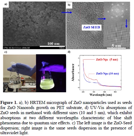
Micrographs of ZnO nanoparticles used as seeds for the nanorods' growth are shown in Fig. 1a, 1b. 5 nm ZnO seeds were obtained at 60 °C according to molars' relations mentioned in the experimental part, ZnO-Nps' size could be increased up to 10 nm by increasing the reactants concentration and reaction temperature. UV-Vis analysis was carried out for the ZnO seeds (both 5 and 10 nm) dispersed in methanol as shown in Fig. (1d); an absorption band around 323 and 346 nm wavelengths is observed for the 5 nm and 10 nm seeds, respectively. This band has a blue-shift due to a quantum size effect of the semiconductor ZnO seeds and is characteristic in metal and semiconductor nanostructures [37].
In this work, both seeds of 5 nm and 10 nm were used to deposit them on PET substrate, which forms a thin film that acts as a growth matrix of zinc oxide nanorods. Corresponding results showed that ZnO-NRs growth is size-independent variation in seed size, and both seeds of 5 and 10 nm produce nanorods roughly with the same dimensions. The above mentioned is explained because of seeds coalescence in solution by the Zn[(NH3)4]2+ absorption on its surface, this absorption depends on the temperature and also of the species concentration in reaction medium. Usually, the control of ZnO-NRs size by hydrothermal methods is accomplished through changes in reactant concentration, reaction time and temperature.
3.3 Seed deposition by Dip-Coating
Despite the many methods for the deposition of ZnO thin film on a substrate; the said ZnO seed film could work as a growth matrix. The most common methods to produce such a ZnO thin films are ALD (atomic layer deposition) [38], thermal evaporation and sputtering [39], etc. Among these, dip-coating is a simple, reproducible, fast and economical method for the seeds' deposition [40]. Hence, the dip-coating method was adopted to produce ZnO seed nanoparticles to achieve a growth matrix for ZnO-NRs production, the substrates were analyzed by SEM and it was found that the size of the thin film formed by the seeds was between 180-220nm, but the actual size of the thin film increased to 240nm due to Zn[(NH3)4]2+ absorption.
3.4 Growth of ZnO nanorods
ZnO-NRs growth was achieved by hydrothermal method in a glass reactor at 65 °C; in this work a stainless steel autoclave was not used. Several pre-attempts were made in order to find the best conditions for obtaining vertically aligned nanorods as follows: i) initially, the growth was carried out by placing the PET substrate with ZnO seeds deposited on (PET/ZnO-NPs) in face-up position at the bottom of the reaction system, ii) subsequently, the substrate was placed in a face-down position in a teflon holder which holds the substrate 5 cm away from the bottom of the reactor, and finally iii) the above treatment was repeated but with the presence of ultrasound.
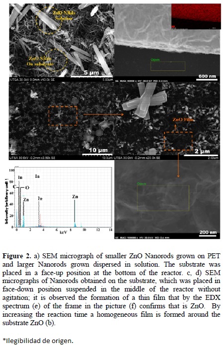
The first experiment results are shown in Fig. 2. One can see two types of ZnO-NRs nanorods with different sizes; some of them have sizes from 300 to 600 nm long and others with sizes greater than 4.00 urn (Fig. 2a). Therefore, it is obvious that there are two types of nanorods growing in the reaction system, those smaller which grow supported by PET substrate and those larger grow and are suspended in the reaction medium, which after the reaction has completed are deposited on the smaller nanorods altering their alignment. In addition, figures 2b, 2c and 2d correspond to the second experiment. In these micrographs, it was observed that the ZnO-NRs grown homogeneously over the whole PET surface, but a film grows on them (Fig. 2c and 2d). EDX spectrum (Fig. 2e) of this area (Fig. 2f) confirms the ZnO peak at 3.7 eV correspond In (Lβ2) of the conducting layer of PET substrate. Otherwise, once reaction time is raised to 10h h ZnO-NRs formed over the entire surface of the film (Fig. 2b). In this way, the three experimental processes such as, NRs deposition on PET; NRs growth in solution, and the thin film formed over ZnO NRs deposited on PET. But, the said third experiment was carried out due to lack of agitation of the reaction system; it's probably the cause of film on ZnO-NRs.
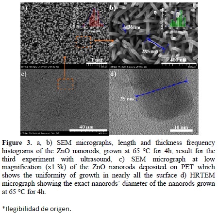
On the other hand, it is possible to obtain nanorods with a thickness less than 25 nm (Fig. 3d) avoiding the seed coalescence by using ultrasound frequency (40 kHz) (third experiment). Ultrasound allows the agitation of the reactant solution and also shakes the substrate while ZnO-NRs grow, hence ZnO thin film on the nanorods is not formed and NRs grow homogenously and vertically aligned throughout the substrate (Fig. 3c). The substrate is not rigid, but flexible; ZnO-NRs orientation on PET/ITO surface is not completely vertical as shown in Fig. 3a, 3b. If it seeks to build flexible devices with this material certain degrees of freedom between the nanorods are required to facilitate their folding. This allows us to assume that the synthesis method used is effective to obtain small nanorods on PET/ITO free of ZnO film and big rods produced in solution. Figure 3a and 3b also exhibit length and thickness frequency histograms of ZnO-NRs obtained with molar ratio 1:1 between the HMT and Zn(NO3)2 at 65 °C for 4h; one can see that length and thickness ranged between 240-285 nm and 25-42 nm; and when they are grown at 8h these values changed to 60-80 nm and 350-400 nm, respectively. However, if the reaction is performed in a discontinuous way it is possible to obtain larger nanorods. For that, the substrate is removed one hour after the reaction has started, so it is washed with deionized water and placed back into the reaction system with a new [HMT and Zn(NO3)2] reactant solution another hour. This process is repeated until the desired size is obtained. The problem now is that when NRs grow too many lose their alignment on the flexible substrate. In rigid substrate like Si(100) these NRs can be obtained to be perfectly aligned.
High-resolution TEM image taken from the square portion in Fig.4b clearly shows the fringes of ZnO (001) plans with the inter-planar spacing of about 0.52 nm and confirms the single crystallinity with the preferential growth in [001] direction (Fig. 4d). Inverse fast Fourier transformation (FFT) analysis confirms that the synthesized nanorods are single crystalline phase with hexagonal wurtzite and grown along [001] direction (Fig. 4c). Simulated images in Fig. 4d show the alignment of atoms seen from the zone axis [100] and Fig. 4c exhibit a hexagonal arrangement because of the nanorods are seen in the zone axis [001] which is the crystal growth direction, Jung et al synthesized ZnO thin films enough to visualize the planes (100) [41].
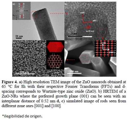
Interestingly the morphologies of synthesized ZnO nanorods like these are an ideal hexagonal ZnO crystal model in which the possible existence of crystal growth velocities in the various crystal facets should be at [0001]>[0111]>[0110]>[0001] [42]. Hence, the growth along the [0001] direction is the maximum and about twice that of [0110]. Therefore, the nanorods were grown along the [0001] direction bound with six crystallographic equivalent [0110] planes. As for the growth habit of ZnO is concerned, it is strongly hemimorphic, thus both the ends of ZnO crystals are bound with the ± (0001) faces. Moreover, it is believed that a fast growing plane generally tends to disappear and leave behind the slower growing forms with lower surface energy. Therefore, the (0001) face is not a surface with equilibrium and it is bound by the growth facets of (0111) which have higher Miller indices but lower specific surface energy compared to the (0001) facets [43-44].
Figure 5a shows a SEM micrograph of ZnO-NRs on PET/ITO substrate, the ZnO thin film formed by ZnO seeds used as growth matrix. The ITO layer of the substrate was confirmed by the EDX spectrum in Figure 5b. After analysis, the substrate is folded slightly and checked by SEM to see the flexion effect on it. The results are illustrated in Figures 5c and 5d. Here it is noted that a slight flexion produces a fracture of the thin film. Even if the substrate is flexible, but the film of ZnO seeds is not, it makes the substrate brittle. This is contradictory, in order to deposit any active material to manufacture flexible devices, the use of theses substrate as working electrode would be limited. Figure 5d shows the cross sectional area of the ZnO thin film where nanorods were grown.
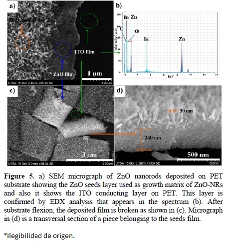
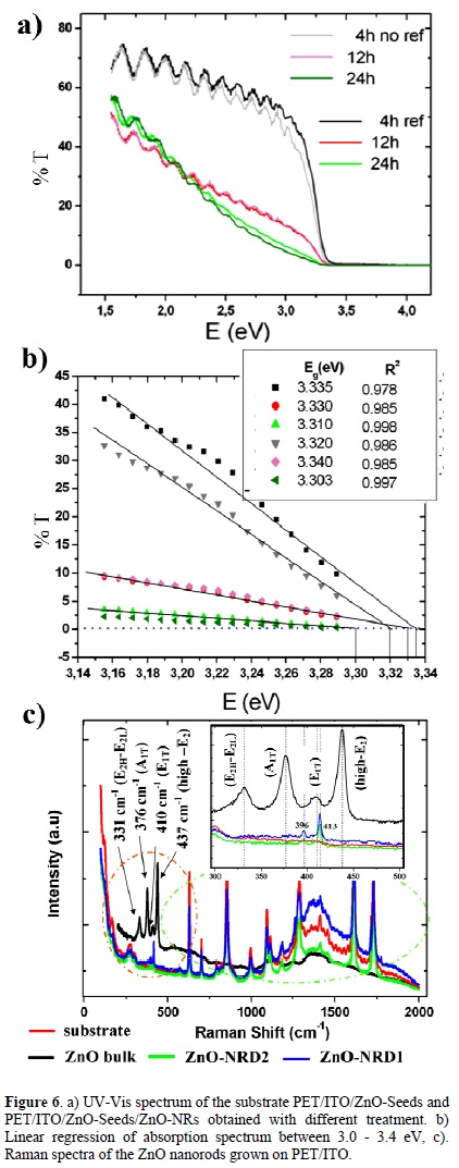
Fig. 6a shows the absorption spectrum of the nanorods deposited on polymer substrates with different treatment. PET/ITO/ZnO seeds and PET/ITO were used as reference sample in order to evaluate the absorption of the seed film deposited on the conducting layer of the substrate. The analyses show that substrates have transmittance above 50% in the visible region, and nanorods' deposits with time reaction (4 h) have a %T around 70%. Transmittance did not vary significantly between PET/ITO/ZnO seeds and nanorods after growth process and, both ZnO nanorods and film formed by ZnO nanoparticles have almost the same visible absorption. This is due to the presence of spaces without nanorods on the polymer surface hence the incident radiation passes directly through it. A more detailed, linear regression was done on an absorption curve in order to determine the band-gap and it was found to be a corresponding value of 3.3 eV approximately, this value does not change significantly in respect to the other treatment in which both diameter and length nanorods are larger (Fig. 6b), the band-gap values determined agree with those reported for bulk zinc oxide [45]. One effective approach to investigate the phase and purity of the low-dimensional nanostructures is micro-Raman scattering. Room-temperature micro-Raman spectroscopy was performed to examine the properties of the ZnO nanostructures. Wurtzite-type ZnO belongs to the space group C46v, with two formula units in primitive cell [46]. The optical phonons at the r-point of the Brillouin zone belong to the representation [46-47]: Topt = (1A1 + 2B1 + 1E1 + 2E2). The phonon modes E2 (low and high frequency), A1 [transverse optical (TO) and longitudinal optical (LO)] and E1 (TO and LO) are all expected to be Raman and infrared (IR) active. The A1 and E1 modes are polar and split into TO and LO phonons with different frequencies due to the macroscopic electric fields associated with the LO phonons. In this experiment, the incident light is normal to the substrate, namely, the incident light is parallel to the c-axis of the nanorods and the Raman signal was recorded in the backscattering geometry. In this configuration, only A1 (LO) and E2 modes are allowed and the other modes are forbidden according to the Raman selection rules [48-49]. The Raman spectrum of the ZnO nanorod arrays was shown in Fig. 5. As expected, only the A1 (TO) mode at 413 cm-1 and E1 (TO) 396 at cm-1 were observed, which further confirms that the ZnO nanorod arrays are highly c-axis oriented.
4. Conclusions
ZnO NRs were synthesized by hydrothermal synthesis assisted by ultrasound. Their dimensions varied between 25 - 80 nm in diameter and 240 - 400 nm in length. NRs' size depended on the synthesis parameters; for that, larger NRs are obtained when the reaction time and temperature increased. NRs were grown on a ZnO rigid film of nanoparticles (seeds) of 5 and 10 nm, which were obtained by wet chemistry and deposited on PET/ITO by dip-coating. NRs' size was independent to the nanoparticles (seed) size. When the PET substrate is flexed the rigid ZnO film is broken affecting its electrical properties, this leads to limitations of these substrates in the elaboration of electronic flexible devices. The synthesis process showed three types of reactions: NRs were grown dispersed in solution, aligned NRs obtained on the PET/ITO substrate and ZnO film grown on aligned NRs, this film grew owing to the absence of agitation in the reaction system. It is evidenced that using the ultrasound hydrothermal system, the ZnO film on NRs is avoided. All of the obtained materials had a ZnO hexagonal wurtzite type structure with [001] preferential growth.
Acknowledgements
The project described was supported by Award Number 2G12RR013646-11 from the National Center for Research Resources, USA. The content is solely the responsibility of the authors and does not necessarily represent the official views of the National Center for Research Resources or the National Institutes of Health and also to PREM grant number DMR 0934218 "Oxide and Metal Nanoparticles the Interface between Life Sciences and Physical Sciences". The authors thank the electronic microscopy laboratory of the International Center for Nanotechnology and Advanced Materials University of Texas at San Antonio and we also thank Dave Olmos from UTSA for technical support and we thank Alma Paola Jose Paola for her assistance in this work.
References
[1] Z.S. Wang, C.H. Huang, Y.Y. Huang, Y.J. Hou, P.H. Xie, B.W. Zhang, H.M. Cheng, Chem. Mater. 13, 678 (2001). [ Links ]
[2] C.H. Liu, J.A. Zapien, Y. Yao, X.M. Meng, C.S. Lee, S.S. Fan, Y. Lifshitz, S.T. Lee, Adv. Mater. 15, 838 (2003). [ Links ]
[3] M.H. Huang, Y.Y. Wu, H. Feick, N. Tran, E. Weber, P.D. Yang, Adv. Mater. 13, 113 (2001). [ Links ]
[4] L.E. Greene, M. Law, J. Goldberger, F. Kim, J.C. Johnson, Y.F. Zhang, R.J. Saykally, P.D. Yang, Angew. Chem. Int. Ed. 42, 3031 (2003). [ Links ]
[5] C. Vargas-Hernandez, F.N. Jimenez-Garcia, J.F. Jurado, V. Henao Granada, Microelectronics Journal 39, 1349 (2008). [ Links ]
[6] F.N. Jiménez-García, D.G. Espinosa-Arbeláez, C. Vargas-Hernández, A. del Real, M.E. Rodríguez-García, Thin Solid Films 519, 7638 (2011). [ Links ]
[7] Z.W. Pan, Z.R. Dai, Z.L. Wang, Science 291 (2001) 1947 [ Links ]
[8] J.Y. Park, D.E. Song, S.S. Kim, Nanotechnology 19, 105503 (2008). [ Links ]
[9] S. Chakrabarti, S. Chaudhuri, Mater. Chem. Phys. 87, 196 (2004). [ Links ]
[10] C.X. Xu, X.W. Sun, Appl. Phys. Lett. 83, 3806 (2003). [ Links ]
[11] J.Y. Lao, J.Y. Huang, D.Z.Wang, Z.F. Ren, Nano. Lett. 3, 235 (2003). [ Links ]
[12] P.X. Gao, Y. Ding, W. Mai, W.L. Hughes, C.S. Lao, Z.L. Wang, Science 309, 1700 (2005). [ Links ]
[13] T. Alammar, A-V Mudring , Materials Letters 63, 732 (2009) [ Links ]
[14] N.R. Pandaa, B.S. Acharya, P. Nayakc, Materialss Letters 100, 257 (2013) [ Links ]
[15] J-F Zhou, J. Ao, Y-Y Xia, H-M Xiong, Journal of Colloid and Interface Science 393, 80 (2013). [ Links ]
[16] Y. Peng, J. Ji, X. Zhao, H. Wan, D. Chen, Powder Technology 233, 325 (2013). [ Links ]
[17] K.-S. Kim, H.W. Kim, Phys. B: Condens. Matter 328, 368 (2003). [ Links ]
[18] K. Ogata, K. Maejima, S. Fujita, S. Fujita, J. Cryst. Growth 248, 25 (2003). [ Links ]
[19] Q. Wan, K. Yu, T.H. Wang, Appl. Phys. Lett. 83, 2253 (2003). [ Links ]
[20] J. Grabowska, K.K. Nanda, K. McGlynn, J.P. Mosnier, M.O. Henry, A. Beaucamp, A. Meaney, J. Mater. Sci. Mater. Electron. 16, 397 (2005). [ Links ]
[21] T. Hirate, T. Kimpara, S. Nakamura, T. Satoh, Superlattices Microstruct. 42, 409 (2007) [ Links ]
[22] Dae-Young Chunga, Jingsong Huangb, Donal D.C. Bradleya, Alasdair J. Campbell, Org. Electron. 11, 1088 (2010). [ Links ]
[23] Jingzhen Shao, Fengjuan Liu, Weiwei Dong, Ruhua Tao, Zanhong Deng, Xiaodong Fang, Songyuan Dai, Mater. Lett. 68, 493, (2012). [ Links ]
[24] C.X. Xu, A. Wei, X.W. Sun, Z.L. Dong, J. Phys. D: Appl. Phys. 39, 1690 (2006). [ Links ]
[25] L. Vayssieres, K. Keis, S. Lindquist, A. Hagfeldt, J. Phys. Chem. B 105, 3350 (2001). [ Links ]
[26] Yan-Xiang Wang, Jian Sun, XueYun Fan, Xi Y, Ceram. Int. 37, 3431 (2011). [ Links ]
[27] D. Polsongkram, P. Chamninok, S. Pukird, L. Chow, O. Lupan, G. Chai, H. Khallaf, S. Park, A. Schulte, Physica B: Condensed Matter. 403, 3713 (2008). [ Links ]
[28] Prabhakar Rai, Hyeon-Min Song, Yun-Su Kim, Min-Kyung Song, Pyong-Rok Oh, Jeong-Mo Yoon, Yeon-Tae Yu, Mater. Lett. 68, 90(2012). [ Links ]
[29] Zhenfeng Zhu, Dong Yang, Hui Liu, Adv. Powder Technol, 22, 493 (2011). [ Links ]
[30] M. F. Meléndrez, K. Hanks, Francis Leonard-Deepak, F. Solis-Pomar, E. Martinez-Guerra, E. Pérez-Tijerina, M. José-Yacaman, J. Mater. Sci. 47, 2025 (2012). [ Links ]
[31] F. Solis-Pomar, E. Martinez-Guerra, M.F Meléndrez, E. Pérez-Tijerina, Nanoscale, Res. Lett. 6, 553 (2011) [ Links ]
[32] L. Vayssieres, K. Keis, S. Lindquist, A. Hagfeldt, J. Phys. Chem. B. 105, 3350 (2001). [ Links ]
[33] X.X. Liu, Z.G. Jin, S.J. Bu, J. Zhao, Z.F. Liu., Mater. Lett. 59, 3994 (2005). [ Links ]
[34] H. Zhang, D. Yang, Y.J. Yi, X.Y. Ma, J. Xu, D.L. Que, J. Phys. Chem. B 108, 3955 (2004). [ Links ]
[35] O. Krichershy, J. Stavan, Phys. Rev. Lett. 70 (1993) 1473 [ Links ]
[36] J.W. Mullin, Crystallization, third ed, Butterworth/Heinemann, p. 1436 (Oxford, 1997). [ Links ]
[37] Y. Chen, X.L. Xu, G.H. Zhang, H. Xue, S.Y. Ma, Physica E: 42, 1713 (2010). [ Links ]
[38] Hisao Makino, Aki Miyake, Takahiro Yamada, Naoki Yamamoto, Tetsuya Yamamoto, Thin Solid Films, 517, 3138 (2009). [ Links ]
[39] Zhenguo Ji, Qinan Mao, Weiqing Ke, Solid State Communications, 150, 1919 (2010). [ Links ]
[40] T. Ratana, P. Amornpitoksuk, T. Ratana, S. Suwanboon, J. Alloy. Compd, 470, 408 (2009). [ Links ]
[41] Z.T. Chen, L. Gao, J. Cryst. Growth 29, 522 (2006). [ Links ]
[42] C. Bundesmann, N. ashkenou, M. Schubert, D. Spemann, T. Butz, E.M. Kaidashev, M. Lorenz, M. Grundmann, Appl. Phys. Lett. 83, 1974 (2003). [ Links ]
[43] C.A. Aguello, D.L. Rousseau, S.P.S. Porto, Phys. Rev. 181, 1351 (1969). [ Links ]
[44] A. Kaschner, U. Haboeck, M. Strassburg, M. Strassburg, G. Kaczmarczyk, A. Hoffmann, C. homsen, A. Zeuner, H.R. Alves, D.M. Hofmann, B.K. Meyer, Appl. Phys. Lett. 80, 1909 (2002). [ Links ]
[45] J. Zhao, Z.G. Jin, T. Li, X.X. Liu, Z.F. Liu, J. Am. Ceram. Soc. 89, 2654 (2006). [ Links ]
[46] Z.W. Pan, Z.R. Dai, Z.L. Wang, Science 291, 1947 (2001). [ Links ]
[47] C. Bundesmann, N. ashkenou, M. Schubert, D. Spemann, T. Butz, E.M. Kaidashev, M. Lorenz, M. Grundmann, Appl. Phys. Lett. 83, 1974 (2003). [ Links ]
[48] C.A. Aguello, D.L. Rousseau, S.P.S. Porto, Phys. Rev. 181, 1351 (1969). [ Links ]
[49] A. Kaschner, U. Haboeck, M. Strassburg, M. Strassburg, G. Kaczmarczyk, A. Hoffmann, C. Homsen, A. Zeuner, H.R. Alves, D.M. Hofmann, B.K. Meyer, Appl. Phys. Lett. 80, 1909 (2002). [ Links ]

