


Servicios Personalizados
Revista
Articulo
 Inglés (pdf)
 Artículo en XML
 Referencias del artículo
 Enviar artículo por email
Indicadores
-
 Citado por SciELO
 -
 Accesos
Links relacionados
-
 Similares en
SciELO
Similares en
SciELO
Compartir

 Permalink
Superficies y vacío
versión impresa ISSN 1665-3521
Superf. vacío vol.26 no.2 Ciudad de México jun. 2013
A methodology for simulation of hybrid Single-electron/MOS transistor circuits
Sarmiento-Reyes A.1, Castro González F. J.1,2†, Hernández-Martínez L.1*
1 INAOE, Electronics Department, Puebla, México. * jarocho@inaoep.mx; fraja@inaoep.mx; luish@inaoep.mx
2† Is currently a PhD student at INAOE.
Recibido: 22 de septiembre de 2012
Aceptado: 27 de abril de 2013
Abstract
On one side, the steady downscaling that CMOS technology has experienced in the last four decades has brought it near its fundamental limits due to the appearance of quantum effects which were not previously taken into account. On the other side, — and even though the current problems involved in their fabrication, nanoelectronic devices such as the Single- Electron Transistors (SET) are devised as future basic cell in the development of electronic systems. It clearly results that in forthcoming years, mature nanometric CMOS devices will share scenario with single-electron devices and other nano-devices in a wide number of applications, yielding hybrid electronic systems. Therefore, it becomes imperative to develop design verification methods and tools specially suited for these hybrid systems. In this paper, we present a simulation methodology for the electrical simulation of hybrid SET/MOS IC designs. The methodology results in a piecewise linear representation of the static SET characteristic that can be easily combined with existing MOS models in a standard industry package for electrical simulation such a SPICE.
Keywords: Single-electron transistor; Hybrid simulation; Piecewise linear modelling.
1. Introduction
In the early days of microelectronic design, a top-to-down design flow was conceived to achieve the designs, while a bottom-up verification path was used in order to check them during every stage of design with the aim of generating a series of EDA tools. In a near future, hybrid systems composed of nanometric CMOS transistors and nano-devices, such as the SET will also need the development of a counterpart of their own design and verification paths. It is regarding the last one, that a simulation methodology is devised in order to determine their electric response.
The main current obstacle when establishing a simulation strategy of hybrid systems consists in dealing with the big gap in development of both worlds, that is to say, the simulation methodology for CMOS circuits is mature even considering the new issues regarding the nanometric dimensions of the devices; while the simulation methodology for SET structures is still in its infancy. A simulation methodology for hybrid systems must cope with this circumstance while providing a reliable verification of the electric behaviour of the MOS/SET circuitry in a scheme that should be appealing for nowadays circuit designers.
By considering this aspect, a particularly straightforward verification strategy for hybrid systems composed of SET devices and CMOS consists in establishing models for the SET that can be easily combined with the MOS models that are embedded in SPICE-like simulators.
1.1. Structure of the SET
A SET consists of two metallic tunnel junctions (Drain and Source) that share a common electrode (Gate), as its symbol shows in Figure 1, [1], [2].

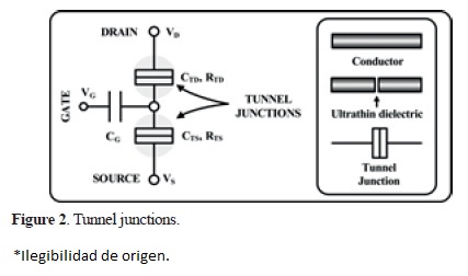
Correspondingly, a tunnel junction is formed — in plain words — by two pieces of metal separated by a very thin insulator, as sketched in Figure 2.
Besides, it turns out that two tunnel junctions in series create a Single-Electron Device (SED) which is the basic cell for Single-Electronics. As a result of the concatenation of the junctions, a third region is located in the middle, the so-called Island — as shown in Figure 3.

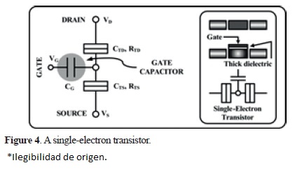
If we connect the island to an external terminal (the gate) via a thick dielectric, then structure of the SET is completed as sketched in Figure 4.
In fact, the structure above constitutes the simplest form of a SET, because actually another structure of SET arises when two external gates are connected to the island [3], [4].
1.2. A glimpse to SET simulation
In the SET, a mechanism of electric charge flow takes place as a result of the discrete nature of the tunneling process, which occurs in multiples of e, the charge of a single electron. Therefore, the analysis of stochastic processes was the most commonly used techniques for simulating SET devices in the early days. However, during the last years, several approaches for simulating the SET have been developed. These efforts can be recast in three categories: Statistical Approach, Master Equation and Macromodelling.
The statistical approach is considered as a low-level simulation method and it is one of the most popular for simulating single-electron structures mainly due to its high precision. It is based on assessing the possibility of a tunnel event via a Montecarlo analysis. Despite its accurate results, simulating large number of structures becomes an extremely slow process, and it does not allow hybrid simulation [5], [6], [7], [8].
The Master Equation approach is considered as a high-level method and it rests on describing the Markov process for the tunneling of a single-electron by establishing a finite number of states. This approach regards each single-electron structure as isolated components in the network and it can combined with MOS circuitry in a rather easy form, but it neglects the needed interconnexions, which conveys errors when used in hybrid simulation [3], [4].
The Macromodelling approach is another high-level simulation method and it is aimed to overcome the problems that arise with the use of the previous methods by resorting to an electric circuit equivalent that can almost directly included in the modified nodal matrix embedded in most of the circuit simulators. It clearly results that hybrid simulation is direct, although it misses insight on the physics of the device [9], [10].
1.3 Using models in electric simulation
Device models are used in electrical simulation in order to represent the set of parameters that characterise a given device.
One can see when and how device models are employed by looking at the standard structure of a circuit simulator [11], as depicted in Figure 5. Herein, the input stage of the simulator achieves — among others — the tasks of parsing the input file, error detection and recovery, and establishing the input data structure. The output stage is mainly focussed on establishing the output display capabilities of the simulator.
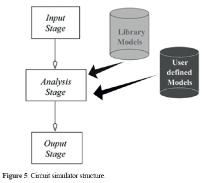
The analysis stage has as main task to establish the equilibrium equation of the circuit and to obtain the solution by resorting to an appropriate numerical engine. It is in this stage where models are incorporated.
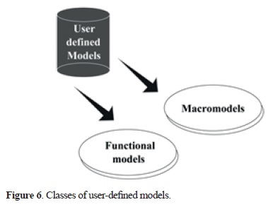
Models usually come in two flavours in most circuit simulation tools: as embedded models within a library or as user defined models. On one side, library models mostly arise from pre-loaded models from IC fabs or specific discrete components. On the other side, user-defined models are given as models that the users have previously developed. The last classes of models offer more flexibility to the user that can be applied on its full extent in order to speed up the simulation by re-using circuit blocks that were previously verified.
Besides, user-defined models are mainly divided into two large categories, namely Macromodels and Functional models —see Figure 6. The first ones are given as sub-circuits or subnetlists that constitute in fact circuit equivalents. The second ones are models stated in a hardware description language, such as VHDL or VERILOG that can recognised by the simulator [12]. Functional models constitute a particularly simple modelling strategy for the case of hybrid systems composed of SET devices and CMOS because the resulting model formulation can be straightforwardly added in any verification flow-path but specially at circuit level.
2. Simulation Methodology
The motivation for achieving a simulation methodology can be established with basis on the previous paragraphs. It clearly results that some techniques above are more suited for simulation at device level, while others are more oriented to circuit level simulation.
With this preamble, the underlying philosophy of our simulation methodology consists in combining the accuracy of the results at device level with the effectiveness of the functional model as a circuit-level simulation technique.
The methodology for simulating hybrid circuits is graphically described in the flow diagram of Figure 7. Hereafter, a step-by-step explanation of the blocks of the methodology is given.
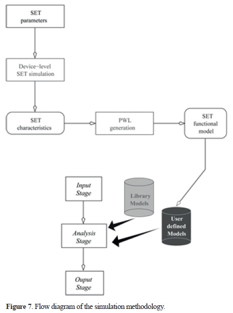
2.1. Device-level simulation
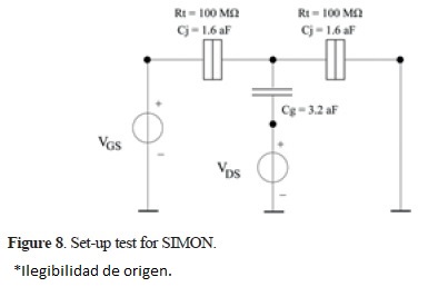
Given the SET parameters, the SET characteristics are obtained by using SIMON —a well-known device-level SET simulator. The parameters of the SET that constitute the input data for SIMON are the values of capacitors and resistors: CTD, RTD, CTS and RTS. The set-up for obtaining the SET characteristics is given in Figure 8, and shows the parameter values. The results of SIMON simulation are shown in Figure 9, where the discrete points of the plots are denoted by small boxes. The characteristics are given as a family of curves IDS- VGS for several values of VDS. Figure 9 (a) shows the characteristics for positive values of VDS while Figure 9 (b) shows the same for negative values of VDS.
(a) For VDS > 0.
(b) For VDS < 0.
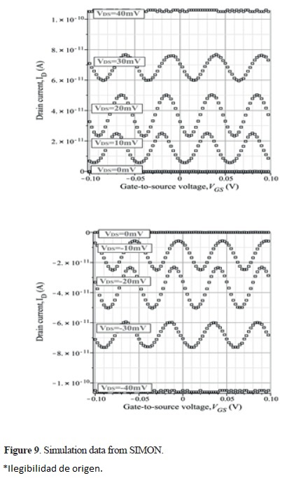
It can be notice that the IDS - VGS characteristics obtained with SIMON, as shown in Figure 9, exhibit a remarkable periodic behaviour that resembles a sinusoid of the form:
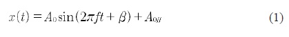
where A0 f, β and Aoff are the amplitude, oscillation frequency, delay and offset, respectively.
2.2. Piecewise linear model generation
PWL modelling approximates continuous i-u branch relationships by means of several linear segments. The main advantage of using PWL models resides in the fact that the resulting equilibrium equations are recast in a set of linear algebraic equations instead of nonlinear algebraic equations, which accelerates the process of finding a solution.
Given a continuous piece-wise linear function, f(x), composed by a finite set of linear segments, its explicit canonical formulation was proposed by Chua and Kang in [13], [14], [15]:
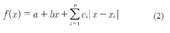
Where the involved coefficients can be calculated as follows:

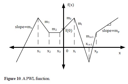
The graphical representation of Equation 1 is given in Figure 10. Herein, a continuous piece-wise linear function, f(x), is formed with p different breakpoints x1< x2< ... < xp. Each segment is defined with a slope mi, where i = 0,1,2, ... , p.
Hereafter, the parameters of the sinusoid in Equation 1 are modelled by PWL representations in order to generate the function in 1 in fully PWL form. Figure 11 shows the behaviours of these parameters as functions of VDS in piecewise linear approximations.
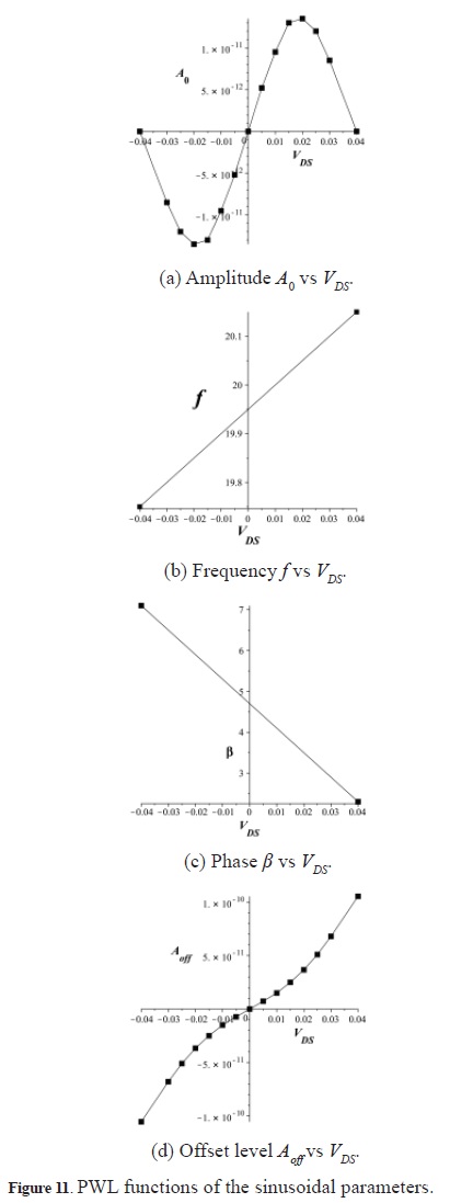
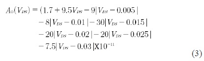
Using the explicit PWL definition of Equation 2, the explicit PWL functions that model the parameters above are given as:


As a result, a closed PWL model of the ID (VGS, VDS) characteristics can be obtained after substituting the previous expressions in Equation 1. Hereafter, the expression for the positive part, i.e. when VDS > 0:

and for the negative part (when VDS < 0):
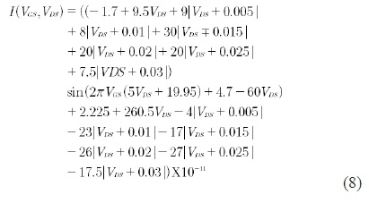
Equations 7 and 8 represent indeed the functional model of the single-electron transistor. By evaluating these equations the continuous plots of Figure 12 have been obtained. In this Figure, the results from SIMON are shown by the square boxes symbols. Our model shows Ids-Vgs characteristics that have an excellent agreement with those generated by SIMON.

Besides, these curves agree with the experimental results from [16], where the Coulomb blockade oscillation phenomenon in a SET is reported.
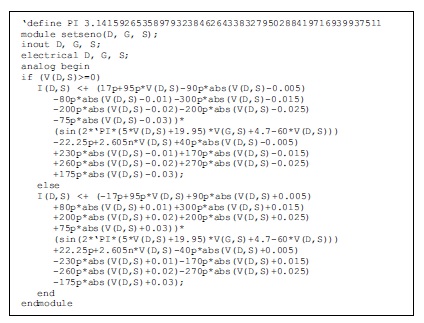
An important advantage of the models expressed in equations 7 and 8 resides in the fact that they can be easily coded in a high-level language such as VERILOG-A in order to carry out hybrid simulation by using a standard circuit-level simulation tool such as SPICE. The next code is a VERILOG-A module ready to be imported by SPICE.
3.Cases of Study
In this section, several only-SET and hybrid circuits are simulated by using the aforementioned model.
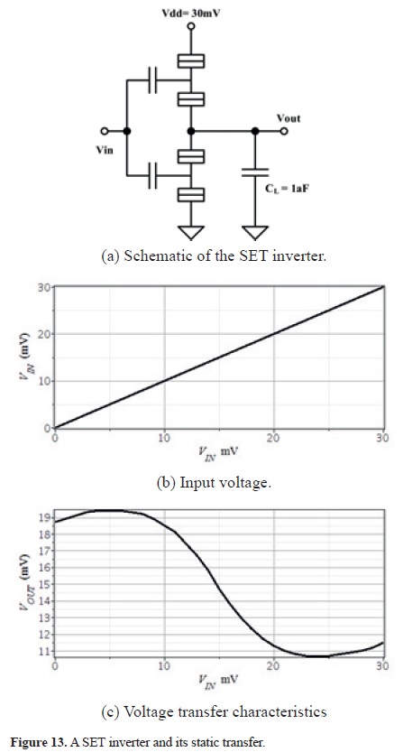
3.1.SET inverter
An inverter is shown in Figure 12-(a). It consists of two identical SETs [17], [18]. The circuit is biased by Vdd source of 30mV, the input voltage is unit ramp, and the output voltage drives a load capacitor of 1aF. The SET parameters are given in Figure 8.
The ramp input voltage is shown in Figure 13-(b). The static characteristics of the SET inverter that are obtained by using our functional model is shown Figure 13-(c).
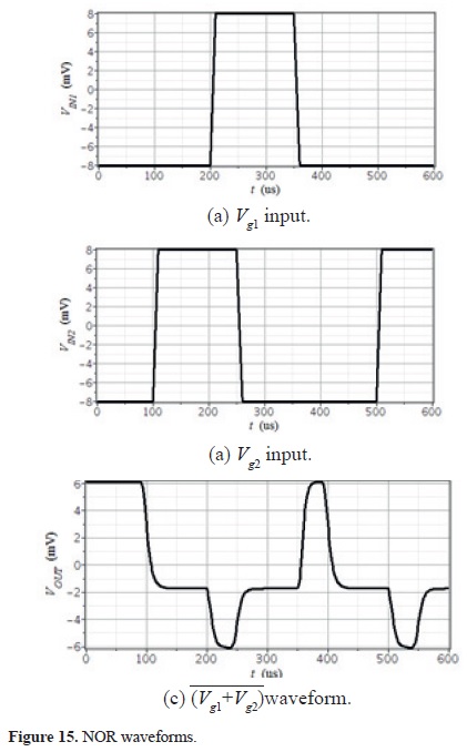
3.2 Single-electron NOR-gate
The next example is a NOR-gate [19] entirely composed of 8 single-electron transistors (from S1 to S8) —as shown in Figure 14. The gate is biased by a ±15mV rail-to-rail supply voltage. The input signals (Vg1, Vg2) are given as ± 8 mV square pulses. The resulting output signal drives a load capacitance of 1aF.
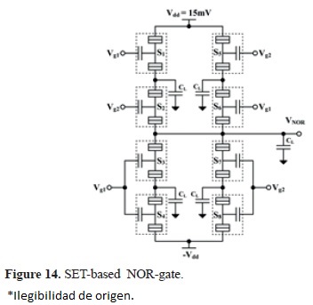
The logic inputs are shown in Figure 15-(a) and Figure 15-(b), while the resulting output waveform is depicted in Figure 15-(c). The output agrees with that reported in [19] where an electrical macro-model of the SET was employed.
3.3 Hybrid NDR
An important basic cell for the design of a wide number of applications, such as oscillator, is the negative differential resistance cell (NDR). In this example, the hybrid NDR from Figure 16-(a) is simulated. The hybrid NDR cell [20] is composed by a MOSFET and a SET in series (see Figure 16-(a)). Vgg constitute a constant bias voltage and Vdd is swept from 0 to 600mV.

The MOSFET acts as a buffer, then, the DC voltage at the drain terminal of the SET remains almost constant and less than e / CΣ , while Vdd is increasing. Therefore, the MOSFET must be working in deep subthreshold region (i.e. Vgg <VTH + e /CΣ , where CΣ = CTD + CTS + CG). Since Vdd is also connected to the gate terminal of the SET, then when Vdd increases, the SET current oscillates, yielding a periodic NDR behaviour.
Electrical simulation of the NDR cell was achieved by combining a traditional model for the MOS transistor with the functional model for the single-electron transistor.
Figure 16-(b) shows that voltage V1 reaches an almost constant value when Vdd is larger than the stipulated condition.
The NDR static characteristic (Id vs Vdd) is plotted in Figure 16-(c). It exhibits several regions of negative slopes which implies locally negative differential resistance. The i - v characteristic of Figure 16-(c) has been contrasted with the results reported in [21], [22], where a steady-state master equation model for the SET was used to simulate a similar NDR cell.
3.4 Hybrid inverter
Figure 17 shows a hybrid inverter circuit formed by a SET driver with an NMOS load [23], [24].
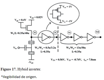
In order to compensate for the low driving-capability of SETs, the inverter is coupled to a CMOS output buffering chain, in order to obtain an output signal with practical amplitude levels.
Similarly, hybrid simulation of the inverter was done by using traditional models for the MOS transistors of the circuit, and our functional model from equation (2) for the single-electron transistor.
Resulting waveforms are shown in Figure 18, for the input voltage Vin, for the inverse output Vt, and for the buffered output V02.
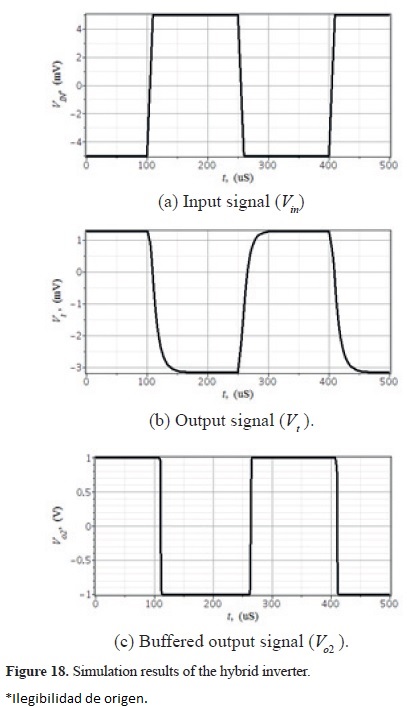
Hybrid simulation results agree with those reported in [24], where the analytical model used for the SET is based on the steady-state master equation, which results much more time consuming than our model.
4. Conclusions
A methodology for the electric simulation of MOS/SET hybrid circuits has been developed. As a result of this, a functional model for the single-electron transistor was obtained by using piecewise linear approximation that yields a closed form for the IDS - VGS characteristic of the SET. The SET model can be easily coded in the VERILOG-A hardware description language and imported by a SPICE-like netlist definition. The feasibility of hybrid simulation methodology has been illustrated by several applications.
References
[1]. R. H. Klunder, PhD Thesis, (Delft University of Technology, 2003). [ Links ]
[2]. J. Hoekstra, R. Van de Haar, Proceedings of European Conference on Circuit Theory and Design, 2, 382, (2003). [ Links ]
[3]. C. H. Hu, J. F. Jiang, and Q.Y. Cai, Proceedings of the 2002 2nd IEEE Conference on Nanotechnology, 483, (2002). [ Links ]
[4]. C. Zhang, L. Fang, B. Sui, Y. Chi, and S. D. Cotofana, Proceedings of the 2nd International Conference on Computer Engineering and Technology, 3, 483, (2010). [ Links ]
[5]. C. Wasshuber, H. Kosina, and S. Selberherr, IEEE Transactions on Computer-Aided Design of Integrated Circuits and Systems, 16, 937, (1997). [ Links ]
[6]. R. Ha. Chen, A. N. Korotkov, and K. K. Likharev, Proceedings of Device Research Conference, 44, (1995). [ Links ]
[7]. Y. S. Yu, J. H. Oh, S. W. Hwang, D. Ahn, Proceedings of Asia Pacific Workshop on Fundamental and Application of Advanced Semiconductor Device, 100, 85, (2000). [ Links ]
[8]. L. R. C. Fonseca, A. N. Korotkov, K. Likharev, Journal of Applied Physics, 78, 3238, (1995). [ Links ]
[9]. Y. S. Yu, S. W. Hwang, D. Ahn, IEEE Transactions on Electron Devices, 46, 1667, (1999). [ Links ]
[10]. Y. L. Wu, S. T. Lin, Technical Proceedings of the 2003 Nanotechnology Conference, 3, 321, (2003). [ Links ]
[11]. J. Ogrodzki, Circuit Simulation Methods and Algorithms, (1994). [ Links ]
[12]. O. Zinke K. Kundert, Kluwer Academic Publishers, (2004). [ Links ]
[13]. P. Julian, IEEE Transactions on Circuits and Systems, 50, 387, (2003). [ Links ]
[14]. D. M. W. Leenarts. M. G. van Bokhoven, Kluwer Academic Publishers, (1998). [ Links ]
[15]. L. O. Chua, P. M. Lin, Computational Methods in CAD, Academic Press, (1973). [ Links ]
[16]. P. Lafarge, H. Pothier, E. R. Williams, D. Esteve, C. Urbina, M. H. Devoret, Journal of Zeitschrift fr Physik B Condensed Matter, 85, 327, (1991). [ Links ]
[17]. R. H. Chen, A. N. Korotkov, K. K. Likharev, Device Research Conference, 44, (1995). [ Links ]
[18]. K. Likharev, Proceedings of the IEEE, 87, 606, (1999). [ Links ]
[19]. Y. S. Yu, Y. I. Jung, J. H. Park, Journal of the Korean Physical Society, 35, 991, (1999). [ Links ]
[20]. C. P. Heij, Applied Physics Letters, 74, 1042, (1999). [ Links ]
[21]. T. Aoki, H. Inokawa, Y. Takahashi, K. Degawa, IEICE Transactions on electronics, 87, 1818, (2004). [ Links ]
[22]. H. Inokawa, A. Fujiwara, Y. Takahashi, Journal of Applied Physics, 41, 2566, (2002). [ Links ]
[23]. K. Uchida, J. Koga, R. Ohba, A. Toriumi, Conference on Solid-State Circuits, 1, 206, (2002). [ Links ]
[24]. K. Uchida, J. Koga, R. Ohba, A. Toriumi, IEEE Transactions on Electron Devices, 50, 1623, (2003). [ Links ]

