


Servicios Personalizados
Revista
Articulo
 Inglés (pdf)
 Artículo en XML
 Referencias del artículo
 Enviar artículo por email
Indicadores
-
 Citado por SciELO
 -
 Accesos
Links relacionados
-
 Similares en
SciELO
Similares en
SciELO
Compartir

 Permalink
Superficies y vacío
versión impresa ISSN 1665-3521
Superf. vacío vol.26 no.1 Ciudad de México mar. 2013
Analysis of threshold voltage fluctuations due to short channel and random doping effects
Jiménez A.*, Ambrosio R. C, Mireles J. Jr., García D. and De la Hidalga F. J.
Electrical and Computer Engineering Department, Instituto de Ingeniería y Tecnología Universidad Autónoma de Ciudad Juárez. *abimael.jimenez@uacj.mx.
Recibido: 21 de septiembre de 2012
Aceptado: 27 de diciembre de 2012.
Abstract
A two-dimensional (2-D) simulation study of short channel and random dopant effects on threshold voltage lowering and fluctuations in 90 nm MOSFET's is presented. The systematic analysis of short channel and random dopant effects was carried out in 2-D on a scale to provide quantitative predictions. Simulations based on a single multigrid solution of the Poisson equation followed by the solution of a simplified current continuity equation are used in the simulations. Both short channel and random dopant effects, on threshold voltage fluctuations are simulated and discussed in MOSFET's. The simulation results will be the start point for the analysis of threshold voltage fluctuations through the comparison with analytical models based on dopant number fluctuations. The simulations show that the threshold voltage fluctuations are principally determined by the fluctuation in the dopant number.
Keywords: Threshold Voltage; Short Channel Effects; MOSFET; 2-D Simulations.
1. Introduction
One of the key design parameters in CMOS technology is the threshold voltage (VTH). For robust circuit design, an accurate estimate of the same is very important. The aggressive scaling of CMOS technology for higher speed and packing density requirements has pushed the device dimensions to such a level where only the 2-D numerical device simulators like MEDICI, SENTAURUS, ATLAS etc. can predict the threshold voltage or any other quantities of interest very accurately. But, such tools are not computationally efficient for VLSI circuit design. The alternative to this is the analytical models, which may even though be approximate but are computationally efficient. In addition, analytical models can provide some insight about the physical processes involved. Basically, there are two general approaches for analytical models for threshold voltage of short-channel devices - charge sharing concept [1-3] and quasi 2-D Poisson's solution [4-5] or a simplified Poisson's equation in the depletion region [6-8].
Because of a number of arbitrary assumptions like the oxide-silicon interface is an equipotential plane over the entire channel length, a trapezoidal depletion charge etc. in a very short channel devices [9] the charge sharing method suffers from two major drawbacks [10]. First, it predicts a 1/L-dependence of the threshold voltage roll-off (ΔVTH) with reduced channel length (L), whereas the experimental results show an exponential increase of ΔVTH with decreasing value of L. Second, it can not predict the VTH fluctuation due to the random channel doping [11-12], which is again a well known fact in channel engineering approach for suppressing the short-channel effects (SCE). In this work, we analyze the VTH behavior due to SCE and Random Dopant Fluctuations (RDF) of a 90 nm n channel MOSFET using 2-D device simulations [13].
2. SCE and RDF
The reduction of VTH for a decreasing channel length and an increasing drain voltage (VDS), is modeled through two SCE, known as Charge Sharing (CS) and Drain Induced Barrier Lowering (DIBL) effects. The CS effect deals with the sharing of the charge in the channel depletion region between the gate and source-drain junctions, while the DIBL is the potential barrier lowering in the Source-Substrate Junction (SSJ). Both effects are modeled through a quasi 2-D analytical solution of the Poisson's equation in the depletion region, considering the depletion approximation and the boundary conditions of φS(0)=Vbi and φs(Leff) = Vbi +VDS (the substrate potential is taken as the ground) [14]:

where VTG = VGS - VTH0 +φs and  is the characteristic length.
The model expressed by (1) can be interpreted as the long channel surface potential modified by the lateral electric field, which is important in short channel devices. In [14] is shown the evaluation of (1) for PD-SOI MOSFETs and the results were compared to 2-D simulations. The conclusion in [15] was that 2-D simulations differ from equation (1), and thus, there is an important variation of the surface potential along the channel even for long channel devices. The surface potential has a minimum at y0 which can be found by solving the equation dφS(y)/dy=0.
The location of y0 and minimum surface potential (φsmin) should be obtained numerically. However, in [12] the value of y0 is approximated by Leff/2, and φsmin is obtained analytically from φSmin = φS(y0)
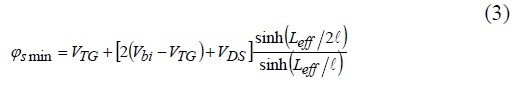
In [12] the approximation y0=Leff/2 is mentioned as to be valid for both, short and long channel devices; however, from PISCES simulations we can see that the location of y0 can not be approximated by Leff/2 in short channel devices [13].
The DIBL effect is present in short channel devices when VDS affects the channel potential profile, lowering the barrier at the SSJ (the potential difference between source and y0), thus allowing carriers to form the inversion channel at a lower VGS than the one expected.
On the other hand, the depletion regions of the SSJ and Drain Substrate Junction (DSJ) overlap the gate depletion region for short channel devices. Thus, the total ionic charge (QB) in the depletion region decreases as the substrate voltage (VBS) increases in the backward direction, but the CS effect should decrease as VBS increases in the forward direction due to the reduction of the depletion region of the SSJ, which results in the increment of QB.
The CS and DIBL models are based on equation (3). In order to determine the threshold voltage, it is assumed that φsmin=2ΦF when VGS = VTH; ΔVTH represents the reduction in the threshold voltage for a decreasing channel length and an increasing VDS:

when ℓ << Leff the threshold voltage roll-off (ΔVTH) can be approximated by

The effect, known as Random Dopant Fluctuation (RDF), is an inevitable consequence of the statistical nature of the doping processes used in current fabrication technology, rendering its elimination impractical. Instead, simulation and analysis techniques are required to fully characterize and mitigate the impact of RDF on transistor and circuit variability.
RDF in MOSFETs results in variation of the threshold voltage, which increases with device scaling. Experimental studies also show that, in short-channel MOSFETs, RDF is the major cause for threshold voltage fluctuation. Not only the variation in the number of dopants but also the shift in their positions in the channel contributes to the deviation of the threshold voltage.
3. Simulation method
A 90 nm channel length n-MOSFET was simulated using SENTAURUS 2-D device simulator. The gate oxide thickness is 4.5 nm, the channel concentration is of 1x1018cm-3. The simulations were based on a 90 nm Bulk technology. To introduce non-uniform channel doping, the channel area is divided into several layers with different doping concentrations along the direction vertical to the channel surface. To introduce the RDF with nonuniform doping, the standard deviation of doping concentration at different channel depths should be calculated. In this case is used the usual definition of the standard deviation of a dataset consisting of N data values as

where is the average or mean of the dataset, as shown in results section. The variance of the dataset is the square of the standard deviation, σ. In SENTAURUS 2-D, Inspect tool is used to display and analyze curves of simulated devices. It features a script language, and an interactive language for computations with curves to determine the standard deviations according to equation (6). Also, SENTAURUS Structure Editor is used to create contacts, to remove the bottom of the substrate, to set the doping concentration of the polysilicon gate, and to define the remeshing strategy, producing the structure shown in Figure 1. Although Figure 1 shows a substrate with a constant doping concentration, which was used to compare with RDF structures. In this figure is also shown the region of RDF where several layers with different doping concentrations were considered.

4. Results
From short channel effects analysis, it is necessary to use a more realistic value for y0 to obtain an improved definition of φSmin. The approximation of y0 = Leff/2 is not valid for short channel devices due to the channel potential profile definitely affect the potential distribution at the source region.
The average doping concentration of the different layers with vertical non-uniform doping is obtained with SENTAURUS simulation. Figures 2 and 3 shows the IDS-VGS curves for 40 devices with different concentrations in the layers and low-drain bias. As can be seen there is an important VTH fluctuation due to the variation in the doping concentration through the layers. As was mentioned before the SCE and the ΔVTH due to these effects depends on both the depletion layer form under the gate and the total ionic charge QB, so the random dopants will change the value of QB in each device. These effects should be modeled accurately for a good representation of electrical behavior of short channel transistors. However, the exact usage of the random number sequence depends on not only the random number of dopants, but also the requested number of samples. Therefore, the random device realization with a certain index out of a sample size of 100 does not correspond to the random device realization with the same index out of a sample size of 1000. To investigate the doping profile of devices that show extreme values of key electrical parameters, the RDF must be used in the simulation that produces the I-V results itself.


5. Conclusions
The short channel effects and random dopant fluctuations were investigated for 90-nm channel length n-MOSFET structures. A more accurate definition of different surface potential must be used in short channel devices. The effects due to random dopant fluctuations are becoming more critical as device dimensions shrink under 90 nm technologies. The results show an important fluctuation of VTH even for devices of 90 nm.
References
[I] Bandy W. R., Kokalis D. P., Solid-State Electron, 20, 675 (1977). [ Links ]
[2] Coe D. J., Brockman H. E., Nicholas K. H. Solid-State Electron; 20, 993 (1977). [ Links ]
[3] Taylor G. W., IEEE Trans Electron Dev 1978;25(3):337-50. [ Links ]
[4] Jean Y. S., Wu C. Y., IEEE Trans. Electron Dev., 44, 441 (1997). [ Links ]
[5] Liu Z. H., Hu C, Huang J. H., Chan T. Y., et al., IEEE Trans Electron Dev., 40, 86 (1993). [ Links ]
[6] Poole D. R., Kwong D. L., IEEE Electron Dev. Lett., 5, 443 (1984). [ Links ]
[7] El-Mansy Y. A., Boothroyd A. R., IEEE Trans Electron Dev., 24, 254 (1977). [ Links ]
[8] Kendall J.D., Boothroyd A. R., IEEE Electron Dev Lett., 7, 401 (1986). [ Links ]
[9] Viswanathan C. R., Burkey B.C., Lubberts G., IEEE Trans Electron Dev., 32, 932 (1985). [ Links ]
[10] Tsividis Y. Operation and modeling of the MOS transistor. (Singapore: Mcgraw-Hill; 2nd ed. 1999). [ Links ]
[11] E. Gnudi, S. Reggiani, E. Gnani, G. Baccarani, IEEE Electron Device Letters, 33, 1453 (2012). [ Links ]
[12] Nauman Z. Butt, Jeffrey B. Johnson, IEEE Electron Device Letters, 33, 1099 (2012). [ Links ]
[13] Sentaurus-Device Version G-2012.06, Synopsys Inc. [ Links ].
[14] Z. H. Liu, C. Hu, J. H. Huang, T. Y. Chan, M. C. Jeng, P. K. Ko, Y. C. Cheng, IEEE Trans. Electron Dev, 40, 86 (1993). [ Links ]
[15] A. Jiménez-P., F.J. De la Hidalga-W, CONCIBE SCIENCE 2009, México. [ Links ]

