


Serviços Personalizados
Journal
Artigo
 Espanhol (pdf)
 Artigo em XML
 Referências do artigo
 Enviar este artigo por email
Indicadores
-
 Citado por SciELO
 -
 Acessos
Links relacionados
-
 Similares em
SciELO
Similares em
SciELO
Compartilhar

 Permalink
Superficies y vacío
versão impressa ISSN 1665-3521
Superf. vacío vol.25 no.3 Ciudad de México Set. 2012
Photocatalytic activity of nitrogen-doped and undoped titanium dioxide sputtered thin films
Franco A. L. M., Zambrano G., Gómez M. E.
Thin Film Research Groups, Department of Physics, Universidad del Valle. Cali Colombia.
Camps E., Escobar-Alarcón L.
Department of Physics, ININ, Apartado Postal 18-1027 México DF 11801, México.
Recibido: 17 de diciembre de 2011
Aceptado: 12 de abril de 2012
Abstract
In the present work titanium dioxide (TiO2) thin films were grown by d.c. reactive magnetron sputtering process, systematically varying the Ar/O2 ratio in the gas mixture, in order to study the influence of the oxygen partial pressure on the crystallographic structure and photocatalytic activity of the Tio2 thin films. After the sputtering process the Tio2 coatings were nitrided in a microwave (f= 2.45 GHz) Electron Cyclotron Resonance (ECR) plasma discharge in pure nitrogen, to compare the photocatalytic activity of undoped and nitrogen-doped Tio2 thin films. The crystal structure of the Tio2 grown samples was studied by x-ray diffraction (XRD) and the presence of the anatase phase in these films were corroborated by Raman spectroscopy. On the other hand, X-ray photoelectron spectroscopy (XPS) measurements carried out in the nitrogen-doped Tio2 samples, showed that the nitrogen was incorporated to the films with an average concentration of 18 at% of N. The UV-Vis optical spectroscopy allowed calculating the band gap. A narrowing of the optical band gap from 3.2 eV for the undoped films to 2.5 eV for the N-doped films was observed. Photocatalytic activity tests were done using a methylene blue (MB) dye solution. The irradiation of the films in the MB dye solution was carried out with an emission lamp in the UV and in the visible range for undoped and N-doped Tio2 films, respectively. The results showed that the N-doped TiO2 films had a higher photocalytic activity in the visible range, reaching a greater MB degradation in comparison with undoped samples, which were subjected to a higher energy radiation.
Keywords: Titanium dioxide; Photocatalytic activity; Magnetron sputtering.
1. Introduction
Titanium dioxide (TiO2) is a semiconductor that is recognized as an efficient photocatalyst due to its excellent functionality, stability and hydrophilicity [1]. However, a main deficiency of TiO2 as a photocatalyst is the wide band gap (3–3.2 eV), and the fact that it is activated only under ultraviolet light irradiation. The change of TiO2 to transform its activity under visible light is one of the most important goals to expand its usefulness in a less expensive way. Many techniques have been examined to achieve this purpose, including the doping of TiO2 with transition metals but these doped materials suffer a thermal instability and increase of the number of carrier recombination centers [2]. Many works describe the nitrogen-doped TiO2 as a more stable material with better properties [3]. There are many different methods to prepare TiO2 films, including sol–gel [4], laser ablation [5], sputtering deposition [6], metal organic chemical vapor deposition [7] among others. In comparison with those methods, the d.c sputtering process presents some advantages, such as the high quality and homogeneity of obtained films. Furthermore, sputtering depositions should be one of the most promising techniques for a large-area of uniform coatings with a high packing density and strong adhesion. On the other hand, the structure and properties of the TiO2 films prepared by d.c. magnetron sputtering, can be modified and controlled via the process parameters like work pressure, sputtering power, substrate bias voltage and oxygen partial pressure. Therefore, a lot of reports have been published on the sputtering deposition of TiO2 films. The present paper investigates the influence of the oxygen partial pressure on the crystallographic structure and photocatalytic activity of TiO2 films obtained by d.c. reactive (Ar/O2) magnetron sputtering, which subsequently are doped using a microwave Electron Cyclotron Resonance (ECR) plasma discharge in pure nitrogen, in order to compare the photocatalytic activity of undoped and nitrogen-doped TiO2 thin films. In this study the photocatalytic activity is evaluated by the degradation of methylene blue (MB), which has often been used as a reactant in semiconductor photocatalysis because this absorbs little light between 300 and 400 nm and its absorption is not overlaped in the region of absorption of TiO2 [8]. The MB is generally used for dyeing cotton, wool, and silk [9] and it has a great number of biological uses. However, given that methylene blue has various harmful effects on human beings, it is of utmost importance to remove it from wastewater [10, 11].
2. Experimental details
The TiO2 films were deposited on quartz and silicon (100) substrates by dc reactive magnetron sputtering system from titanium (99.9%) target with 2.54 cm of diameter, placed inside a chamber with an Ar/O2 gas mixture. The Ar/O2 ratio in the gas mixture was varied systematically (95/5, 90/10, 80/20 and 50/50) in order to study the influence of the oxygen partial pressure on the crystallographic structure and photocatalytic activity of the TiO2 thin films. The base pressure was 4x10⁻⁴ mbar and the working pressure (2.4x10⁻² mbar), power applied to the target (150 W), distance from the substrate to the Ti target (8 cm), temperature (400 °C) and deposition time (2 hours), were maintained constant for all samples.
After the sputtering process the TiO2 films were treated in pure nitrogen plasma using a microwave Electron Cyclotron Resonance (ECR) discharge. In the experiments described, a constant power of 400W was used. The ultimate pressure of 2.7×10⁻⁶ mbar was obtained using a 200 ls−1 turbo molecular vacuum pump. The nitrogen plasma was created at a nitrogen pressure of 1.3×10⁻³ mbar. A single Langmuir probe was used to take radial profiles of the plasma parameters (electron temperature, density, floating and plasma potential) in a region of the reaction chamber close to the sample holder. For the treatments of the TiO2 films a plasma density of 2×1011 cm−3 was used [12]. The substrate temperature and the treatment time were kept constant at 300 °C and 15 min, respectively.
The crystal structure of the TiO2 films was determined by using glancing angle X-ray diffraction (GAXRD) at 2° incidence angle in the 2-theta mode over the range of 20°<2ϑ <80° with a Bruker (Model D8 Advance) diffractometer using the Kα1 line of Cu (λ = 1.5406 Å, 25 kV and 16 mA). The crystallite size was deduced from the full width at half maximum of XRD lines according to Scherrer equation [13].
X-ray photoelectron spectrometer spectroscopy (XPS, Multilab ESCA 2000) was used to analyze the surface element composition. All the XPS spectra were calibrated with the C1s peak at 284.6 eV. A Jobin Yvon micro-Raman system was used to obtain the Raman spectra. A Nd:YAG laser (λ = 532 nm) was used to induce the Raman scattering. An Olympus BX-41 optical microscope was used to focus the laser beam on the sample and collect the scattered light. A Cary 5000 spectrophotometer by Varian was used to obtain the transmittance of the films in the UV–Vis range and a Shimadzu spectrophotometer UV model 1601was used in the photocatalytic tests.
3. Results and discussion
3.1. Raman analysis
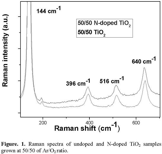
The figure 1 shows the Raman spectra corresponding to the undoped and N- doped TiO2 films growth at 50/50 of Ar/O2 ratio. The Raman results indicate that only the anatase phase is formed under the conditions described above. The spectra are constituted by a peak located at 144cm−1 and three bands at 396, 516, and 640 cm−1. This spectrum is in good agreement with the results reported for the TiO2 sputtered films crystallized in the anatase phase [14]. It can be observed that the Raman spectra of the N-doped TiO2 film has the same bands described for the TiO2 film, indicating that structurally, the material does not change after the treatment in the ECR nitrogen plasma.
3.2 XRD structural analysis
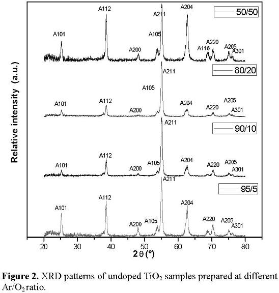
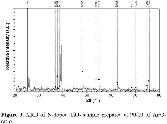
The XRD patterns for undoped TiO2 films deposited on quartz substrates are presented in Figure 2. The crystallite size of the samples calculated from Scherrer equation were 18.6, 18.6, 17.9 and 17.7 nm for the films deposited at 95/5, 90/10, 80/20 and 50/50 of Ar/O2 ratio, respectively. From the XRD patterns we can observe that the undoped TiO2 films have a (211) (peak noted A211) preferred orientation in the anatase crystalline structure. The commonly reported anatase phase orientation is (101). This behavior is attributed to the fact that different surface free energies are associated to the different reflection planes [15]. In the present case the sputtering power density (∼300 kWm-2) activates the TiO2 film growth from a relative lower surface free energy to a higher surface free energy [16]. XRD diffractogram of the N-doped film growth at 90/10 of Ar/O2 ratio is shown in figure 3. This XRD pattern is similar to the patterns for the non nitrided sample. The Bragg peaks correspond to the anatase phase. The preferred orientation changes to the (1 1 2) reflection plane, probably due to the fact that during the nitriding process the sample was heated to 300 °C. Although the temperature is too low to produce a phase change, it can cause a relaxation of the internal stresses in the material, generating a change of the preferred orientation in the TiO2 film. We also observe at the N-doped pattern a shift to the right of the Bragg peaks given by the distortion of the lattice caused by the incorporation of the nitrogen atoms [17]. The crystallite size of the samples calculated from Scherrer equation are 36.0, 35.8, 34.9 and 34.6, nm, for the sample growth at 95/5, 90/10, 80/20 and 50/50 of Ar/O2 ratio, respectively. The crystallite size increases in comparison with the undoped samples indicating that crystallinity improves after the nitriding process.
3.3 Optical properties
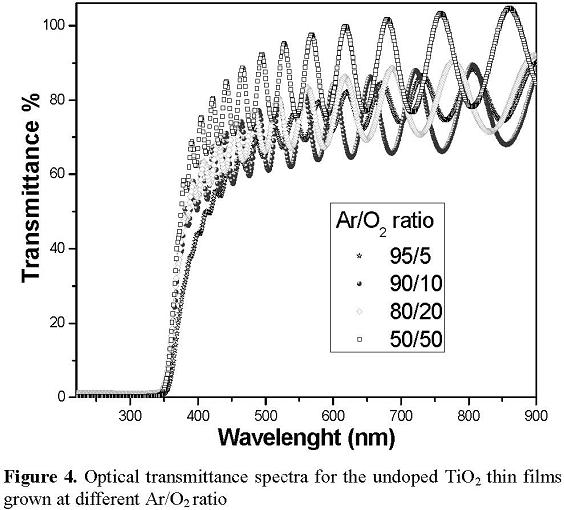
Figure 4 presents the optical transmittance spectra in the 200–900 nm wavelength range for the undoped TiO2 thin films grown at different Ar/O2 ratio. All the films were highly transparent with a transmittance greater than 70% in the visible range of the electromagnetic spectrum and present a sharp cut off at approximately 370 nm. Assuming that the TiO2 and N-doped TiO2 films have an indirect semiconductor band gap, the optical bang gap of the films can be determined using the Tauc approach [18]. The Tauc plot of (αhν)1/2 as a function of the photon energy allows to evaluate the indirect band gap of the films by extrapolating the straight line part of the curves to (αhν)1/2 =0. The band gap for the undoped TiO2 film was estimated to be 3.2 eV for all samples. Within the accuracy of the Tauc approach, the value of the optical band gap agrees well with the reported value of anatase thin films (3.2 eV). The band gap of the N-doped TiO2 films (plots not shown) were 2.1, 2.6, 2.3 and 2.2 eV at 95/5, 90/10, 80/20 and 50/50 of Ar/O2 ratio, respectively. These results demonstrate that the doping with nitrogen cause a narrowing of the band gap of the TiO2 semiconductor, suggesting that the obtained films could be active in the visible light range.
3.4 XPS analysis
The samples were analyzed by XPS (X-Ray Photoelectron Spectroscopy) without etching and with etching by means of Ar+ ion bombardment with energy of 3kV for 5 min on a 25 mm² area of samples. In figure 5 we can see the XPS spectra of N-doped TiO2 films after the etching process with Ar + ions. Fig. 5 shows the characteristic peaks associated to the Ti 3s, 2p, 2s bonds, O 1s bond and N 1s bond. Additionally in the spectra appears a small Ar 2p peak at (241.8 ± 0.7) eV, due to the fact that some Ar ions were implanted into the surface samples after etching. It could also be identified a peak located at (284.5 ± 0.7) eV associated to C 1s which is attributed to the hydrocarbons (C-C, C-H) bonds and another small peak at (289.4 ± 0.7) eV attributed to the C = O bonds [19]. These two peaks usually occur for any contamination that follows when the specimens are removed from the deposition chamber. This is corroborated by the appearance of the 530.6 eV peak associated to the O in the C = O bonds [15]. From these spectra (see Fig. 5) it is observed a slight shift to lower energies that are reported for Ti 2p level of Ti-O bond, in comparison with the Ti 2p peak of 95/5 sample located at (457.9 ± 0.7) eV.
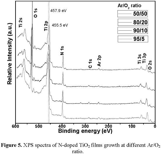
The shift in the energy of this bond in the N-doped TiO2 films suggests that the TiO2 lattice structure is modified by the substitution of O atoms by N atoms due to the covalent bond between the N and Ti. For the samples deposited with a higher oxygen concentration in the Ar/O2 gas mixture (80/20 and 50/50) this shift is greater. This fact is consistent with other reported works in which this fact demonstrates the formation of Ti-O-N bonds by the partial substitution of O atoms by N atoms in the TiO2 lattice [20]. The chemical composition analysis by XPS can be seen in Table 1. As it is required in the present work that the nitrogen concentration in the films remains constant, the plasma density (2 x 1011 cm-3) and the substrate temperature (300 ° C) parameters were kept constant during the treatment of the TiO2 samples in pure nitrogen plasma. In fact, the chemical composition results show that the percentages of N were not significantly different from one sample to another.
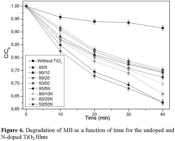
3.5 Photocatalytic analysis
For the photocatalytic measurements the variation of the concentration of the Methylene Blue (MB) dye, was followed by the change (a decrease) of the intensity of the characteristic band in the UV–Vis transmittance spectra of the MB, located at 665 nm, which was analyzed as a function of the irradiation time. The MB solution in a quartz cell was irradiated with ultraviolet light and an incandescent lamp (both with a power of 4 W), for the undoped and N-doped TiO2 films located 4 cm from the cell. The solution was bubbled with air before irradiation. Photocatalytic performance was evaluated from these measurements by analyzing the percentage of dye degradation when the films were used as a catalyst. The undoped samples showed photocatalytic activity but not significant changes between them were observed. The comparison of the N-doped samples results are shown in Figure 6. From this figure it is also observed that the N-doped samples present more photocatalytic activity than the undoped samples. These results show that the substitution of O atoms by N atoms (previously demonstrated by the XPS results) in the TiO2 films is an important factor for films to have a response to visible light, because this substitution reduces the band gap to absorb light in the visible region and acts as an efficient photocatalyst even under visible light. This reduction can be attributed to the change of the top of the valence band through the hybridization of the atoms of the substituted nitrogen 2p and oxygen 2p orbitals, giving rise to acceptor states of N 2p localized over the valence bands, which are mainly composed of O 2p states [21]. Recent theoretical and experimental studies [22-24] have given strong evidence that nitrogen as dopant introduces intermediate discrete states above the gap edge of the valence band of TiO2. For the excitation of the visible light photons, the electrons are promoted to the conduction band, while the holes remain in the intermediate states of the gap. Due to the discrete nature of these intermediate states, the mobility of holes generated by visible light is much lower than the mobility of holes generated by the ultraviolet light in the valence band [25]. As a consequence, the holes generated by visible light have a lesser recombination rate for an oxidation reaction at the interface of the film. The holes move from the valence band slowly through the intermediate states and thus, the mobility gap is strongly influenced by the width of these intermediate states. For this specific case of nitrogen-doped TiO2 films, the migration of the holes through the intermediate states is slower, and for this reason the hole can take a greater time to migrate from the interior to the surface. This time can be comparable or even larger than the time to transfer electrons from the band driving to oxygen. Then, this process improves the photocatalytic activity of films because the time of electron hole pair recombination increases, with this allowing it to be in the process of oxidation on the surface [25].Comparing the photocatalytic activity results of our TiO2 thin films, for instance, with obtained by using boron-doped TiO2 nanoparticles, the last present higher activity, which was explained in terms of such factors as small crystal size, high surface area, mesoporous structure, and the formation of Ti(III) [26], aspect which does not present a supported catalyst, but in comparison, the TiO2 films can be removed easily from a solution and the nanoparticles not. On the other hand, Fe-doped TiO2 nanoparticles displayed a red shift in the band gap transition with the increase of Fe content inserting into the TiO2 matrix, but their photoactivity degradation on MB, decreased. [27]. Likewise, Fe or Cr-doped TiO2 films grown by sol-gel, showed a red shift absorption too, extended to 496 and 434nm corresponding to the band gap energies of 2.50 eV and 2.86 eV, respectively [28], but as can be seen from this study, our nitrogen-doped TiO2 thin films exhibited a change of the band gap energy to 2.1 eV.
4. Conclusions
TiO2 films were deposited on quartz and silicon substrates by dc reactive magnetron sputtering and doped in a microwave Electron Cyclotron Resonance (ECR) plasma discharge in pure nitrogen. Raman and XRD analysis indicate the formation of the anatase phase under our experimental conditions, and XPS confirmed that the doped films have nitrogen substituted at some of the oxygen sites in the TiO2 lattice, which formed a narrow N 2p band above of the valence band. The band gap of the N-doped TiO2 thin film containing 18 % N decreased until 2.1 eV. Finally the photocatalytic tests showed that the N-doped TiO2 films have a greater photocatalytic activity in the visible light range in comparison with the undoped TiO2 samples, however that the doped films were irradiated with a lower energy.
Acknowledgements
To the Mexican National Institute for Nuclear Research (ININ) for all the support granted in the course of this work. This work is partially supported by "El Patrimonio Autónomo Fondo Nacional de Financiamiento para la Ciencia, la Tecnología y la Innovación Francisco José de Caldas", contract RC - No. 275-2011 and Universidad del Valle, research project No 7703.
References
[1]. D. Mardare, D. Luca, C.-M. Teodorescu, D. Macovei, Surface Science. 601, 4515(2007). [ Links ]
[2]. A. K. Ghosh, H. P. Maruska, J. Electrochem. Soc. 124, 1516(1977). [ Links ]
[3]. S. Sato, Chem. Phys. Lett. 123, 126(1986). [ Links ]
[4]. J. Yu, X. Zhao, Mater. Res. Bull. 35, 1293(2000). [ Links ]
[5]. S. Somekawa, Y. Kusumoto, M. Ikeda, B. Ahmmad, Y.Horie. Catal. Commun. 9, 437(2008). [ Links ]
[6]. Z. Qinnan, L. Baoshun, Z. Xiujian, Rare Met. Mater. Eng. 32, 339(2003). [ Links ]
[7]. A.-M. Lazar, D. Chaumont, Y. Lacroute, M. E. Gómez, J. C. Caicedo, G. Zambrano and M. Sacilotti, Phys. stat. sol. (a) 205, 289(2008). [ Links ]
[8]. A. Mills, J. Wang, J. Photochem. and Photobiol. A: Chem. 127, 123(1999). [ Links ]
[9]. S. Senthilkumaar, P.R. Varadarajan, K. Porkodi, C.V.Subbhuraam, J. Colloid Interface Sci. 284, 78(2005). [ Links ]
[10].M. Berrios, M. Á. Martín, A. Martín, J. Ind. Eng. Chem. 18, 780(2012). [ Links ]
[11].X. Jin, M. Jiang, X. Shan, Z. Pei, Z. Chena, J. Coll. and Int.Sci. 328, 243(2008). [ Links ]
[12].Enrique Camps, Fernando Becerril, Stephen Muhl, O. Alvarez - Fregoso, M. Villagrán. Thin Solid Films. 373, 293(2000). [ Links ]
[13].D. Mardare, M. Tasca, M. Delibas, G.I. Rusu, Appl. Surf.Sci. 156, 200(2000). [ Links ]
[14].A. Arias, J. C. Caicedo, L. Ipaz, W. Aperador, L. Tirado-Mejía, G. Zambrano, M.E. Gomez, Rev. Latinoamericana deMetal. y Mater. S1 4, 1479 (2009). [ Links ]
[15].M. Lazzeri, A. Vittadini, A. Selloni, Phys. Rev. B 65, 119901 (2002). [ Links ]
[16].P. Singh, D. Kaur. Physica B. 405, 1258 (2010). [ Links ]
[17].H. Sun, Y. Bai, W. Jin, N. Xu. Solar Energy Materials & Solar Cells. 92, 76 (2008). [ Links ]
[18].J. Tauc, Amorphous and Liquid Semiconductors, (Plenum Press, London, 1974). [ Links ]
[19].L. Zhu. J. Xie. X. Cui. J. Shen. X. Yang. Z. Zhang. Vacuum.84, 797 (2010). [ Links ]
[20].Enrique Camps, L. Escobar-Alarcón, Marco Antonio Camacho-López, Dora A. Solis-Casados, Materials Science andEngineering B. 174, 80 (2010). [ Links ]
[21].Z. Lin, A. Orlov, R. M. Lambert, and M. C. Payne. J. Phys.Chem. B. 109, 20948 (2005). [ Links ]
[22].K. Yang, Y. Dai, B. Huang. J. Phys. Chem. C. 111, 12086 (2007). [ Links ]
[23].G. R. Torres, T. Lindgren, J. Lu, C. G. Granqvist, S. Lindquist, J. Phys. Chem. B. 108, 5995 (2004). [ Links ]
[24].H. Irie, Y. Watanabe, K. Hashimoto. J. Phys. Chem. B. 107, 5483 (2003). [ Links ]
[25].X. Zhang, K. Udagawa, Z. Liu, S. Nishimoto, C. Xu, Y. Liu, H. Sakai, M. Abe, T. Murakami, A. Fujishima. J. Photochem. Photobiol A: Chem. 202, 39 (2009). [ Links ]
[26].R. Khana, S.W Kima, T.J Kima, C.M. Namb, Mater. Chem.and Phys. 112, 167 (2008). [ Links ]
[27].Z. Li, W. Shen, W. He, X. Zu. J. of Hazard. Mater. 155, 590(2008). [ Links ]
[28].S. Buddee, S. Wongnawa, U. Sirimahachai, W. Puetpaibool, Mater. Chem. Phys. 126, 167 (2011). [ Links ]

