


Serviços Personalizados
Journal
Artigo
 Inglês (pdf)
 Artigo em XML
 Referências do artigo
 Enviar este artigo por email
Indicadores
-
 Citado por SciELO
 -
 Acessos
Links relacionados
-
 Similares em
SciELO
Similares em
SciELO
Compartilhar

 Permalink
Superficies y vacío
versão impressa ISSN 1665-3521
Superf. vacío vol.25 no.2 Ciudad de México Jun. 2012
Semiconductor Nanocrystals of InP@ZnS: Synthesis and Characterization
Arias-Cerón J. S.
Centro de Investigación en Ciencia Aplicada y Tecnología Avanzada del IPN, Unidad Legaria Calz. Legaria 694, Col. Irrigación, México D. F. 11500, México
González-Araoz M. P.*
Centro de Investigación en Biotecnología Aplicada, IPN, San Juan Molino Km 1.5 de la Carretera Estatal Sta. Inés Tecuexcomac-Tepetitla, Tlaxcala 90700, México
Bautista-Hernández A.
*Facultad de Ingeniería, Universidad Autónoma de Puebla Puebla, Pue. 72570, México
Sánchez Ramírez J. F., Herrera-Pérez J. L.
Unidad Profesional Interdisciplinaria en Ingeniería y Tecnologías Avanzadas del IPN Barrio Laguna Ticomán, México D.F. 07340, México
Mendoza-Álvarez J. G.
Departamento de Física del Centro de Investigación y de Estudios Avanzados del Instituto Politécnico Nacional Apdo. Postal 14-740, México D. F. 07000, México
Recibido: 22 de febrero de 2012
Aceptado: 3 de junio de 2012
Abstract
Colloidal dispersions of InP@ZnS nanoparticles were prepared using a single-step heating-up method relying at low temperature. The obtained particles are highly crystalline, monodisperse and exhibit size-dependent radiative emission in the range of 329−480 nm. By simply varying the concentration of the molecular precursor, the particles size can be controlled in the range from about 1.1 to 4.5 nm. The formation of InP nanocrystals has been confirmed using the techniques TEM, HRTEM, PL and UV-Vis spectroscopy.
Keywords: Nanocrystals Synthesis; Semiconductors; Optical properties.
1. Introduction
Motivated by new and interesting properties that present the matter at the nanoscale dimensions [1], several studies have been focused on the implementation of methods of preparation of nanoscale particles [2-3]. In particular, the synthesis and characterization of semiconductor nanocrystals (NCs) is so important not only to understand its extraordinary properties that become dominant at the nanoscale [4], but for their application in the development of technologies for new devices such as: LEDs [5], lasers [6], transistors [7], waveguides [8] and solar cells [9].
Group II-VI NCs have been the most studied due to their interesting luminescent properties covering the whole visible spectra [10-11]. Unlike the II-VI NCs that are already commercially available, NCs of the group III-V exhibited better optical properties for applications in areas such as biology and medicine. The presence of covalent bonds, little toxicity to the environment, specific features of excitation, radiative emission taking place in the visible and near IR range, resistance to degradation, high extinction coefficients, as well as the great possibility of bio-conjugation, make the III-V NCs ideal candidates for the development of new luminescent biomarkers [12-14].
At present, indium phosphide (InP) is one of the most promising compounds in this context [15].
Although currently there are chemical methods for the synthesis of NCs, these have been implemented mostly for the II-VI group semiconductors [16]. For the case of III-V semiconductors, probably because of their high degree of covalent bonding, few efforts have been made to develop simple and reproducible methods that are capable of generate nanocrystals with well-defined properties [17-19]. The control of the surface characteristics of the NCs is also important in terms of improving their optical properties and biocompatibility [20].
While some chemical methods such as the dehalosilylation and the hot-injection method [21-24] have been used for the synthesis of InP NCs [25-27], there are still problems that must be solved to obtain highly luminescent nanoscale particles. Methods of surface passivation of InP NCs with HF [28] or by the growth of a ZnS shell [29] have been the best alternative to obtain nanocrystals with improved fluorescence properties.
Based on the background and with the goal of having a control on the formation and the luminescent properties of the NCs, we report in this article the results of the controlled synthesis of InP semiconductor nanostructures with ZnS surface passivation. InP@ZnS core/shell nanocrystals were synthesized using a practical and simple chemical method. We also show the effect of the temperature of synthesis on the formation of the InP@ZnS nanostructure. The structural and optical properties of the nanoparticles were characterized using techniques such as transmission electron microscope (TEM) and high resolution TEM (HRTEM), UV-Vis absorption and photoluminescence (PL) spectroscopies.
2. Experimental
2.1. Chemical
Indium acetate (InAc3) myristic acid (MA), 1-octadecene (ODE), 1-dodecanethiol (DDT), tris (trimethylsily) phosphine (P(TMS)3) and zinc stearate were purchased from Sigma-Aldrich and used as received.
2.2. Synthesis
InP@ZnS nanocrystals were synthesized and stored in a glove box using a single-step procedure without precursor injection according to the procedure adopted by Liang Li et al [30], at different temperatures. First, the precursor of indium (indium myristate, In(MA)x) was prepared by mixing 0.1 mmol of InAc3 under inert atmosphere with 0.3 mmol of myristic acid and 5.0 g of ODE in a 50 mL threeneck flask equipped with a condenser. The mixture was heated to 100 °C for 1 h under vacuum to obtain an optically clear solution, backfilled with Ar gas, and cooled down to room temperature. Then, 0.06 mmol of In(MA)X, 0.06 mmol of zinc stearate, 0.06 mmol of DDT, 0.06 mmol of P(TMS)3 and 8 ml of ODE were stirred under inert atmosphere in a three-neek flask equipped with a condenser. The mixture was then heated at different temperatures 100 (sample S1), 150 (sample S2), 200 (sample S3) and 270 °C (sample S4) for 1 h and the temperature was then decreased to room temperature. The nanocrystals were then purified with a chloroform/ methanol/acetone (1:1:10 in vol) mixture followed by centrifugation, to remove the starting materials and side products. The resulting precipitates were dispersed in chloroform.
2.3. Measurements
Room-temperature optical absorption spectra of the colloidal samples were recorded using a 10 mm path length quartz cuvette in a UV-Vis-NIR scanning spectrophotometer (Shimadzu UV 3101PC double beam). The PL spectra were obtained using a He-Cd (Omnichrome–Series 56) laser emitting at 325 nm with an optical excitation power of ~15 mW at room temperature. The radiative emission from the sample was focalized to the entrance slit of a HRD-100 Jobin-Yvon double monochromator with a resolution better than 0.05nm, and detected with an Ag-Cs-O Hamamatsu photomultiplier with a spectral response in the range 350-1000 nm. For electron microscopy analysis, two microscopes, a Jeol JEM200 and a Tecnai 200 TEM, were used for the lowmagnification and high-resolution observations of the samples, respectively. High-resolution electron microscope (HRTEM) images were digitally processed by using filters in the Fourier space. For transmission electron microscopy (TEM) observations, a drop of colloidal solution was spread on a carbon-coated copper microgrid and dried in vacuum.
3. Results and Discussion
Nanoparticles of semiconductor materials such as InP in the nanoscale strongly absorb light when the excitation energy is greater than the bandgap energy. During this process, electrons are promoted from the valence to the conduction band. Measurements of UV-Vis spectra reveal a large number of energy states in the NCs [31]. The lowest excited energy state is shown by the first observable peak in the absorption spectrum, known as the quantumconfinement peak. The energy of the quantum-confinement peak depends on the size, shape and structure core@shell [32].
While techniques like TEM and HRTEM reveal the exact size and structure of those nanoparticles, optical absorption spectra give a quick and gross idea on their sizes and structures. In this study, we used TEM, and HRTEM, along with optical absorption spectroscopy and PL to study the size, size distribution, and fine structure of semiconductor InP@ZnS colloids formed at different temperatures.
3.1. Optical Absorption
Figure 1 (2) shows the absorption spectra for the NC's colloidal samples S1, S2, S3 and S4. All spectra were recorded at room temperature.
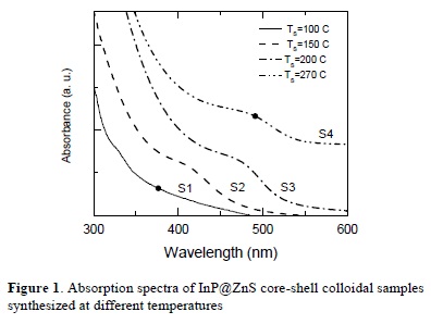
It is clear from Figure 1 that the samples exhibit absorption edges which are red shifted when increasing the synthesis temperature. The red shift of the absorption edges of nanocrystals arises from increasing particle size. The band gaps of the samples were determined using the relation:

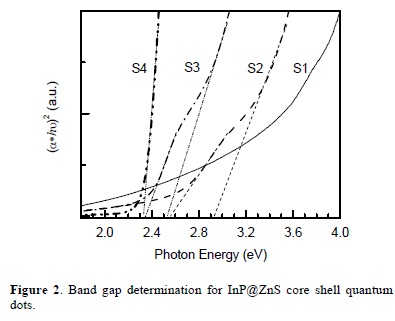
where α is a absorbance, C is a constant, Eg is the band gap energy of the material and the exponent n depends on the type of transition [33], for direct transition we take n=1/2. The value of the optical band gap energy is calculated by the extrapolation of the straight line portion of (αhν)2 vs. hν graph (Fig. 3) to the hν axis.
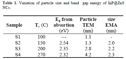
The obtained band gap energy values of the samples are: 2.32 eV for S4, 2.35 and 2.49 eV for S3, 2.54 and 2.93 eV for S2; the band gap for S1 sample is difficult to assess. Values of the band gap energy are higher than the bulk band gap energy of InP (1.27 eV) giving the evidence of the quantum confinement effects in the InP quantum dots.
The shift in the band gap energy as determined from the absorption spectra, might also be used in determining the nanoparticle size (dg) using the effective mass approximation (EMA) relation [33]:
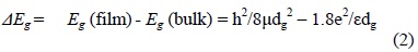
where: 1/μ = 1/mh + 1/mh is the effective electron-heavy hole mass. For cubic InP, me = 0.075 mo, mh = 0.60 mo and ε = 12.40 is the permittivity of the sample and Eg(bulk) is 1.27 eV at 300 C [34]. The particle size values obtained from this last equation are shown in Table I.
In order to determine the effects of the reaction temperature in the synthesis of the nanoparticles, TEM analysis has been performed. In Figure 3, typical TEM micrographs of the semiconductor nanoparticles and their respective size distribution histogram are presented; in this case, it corresponds to the sample S4, grown at a temperature of 270 C. For built up the histogram, the size of more than 60 particles was measured. The size distribution follows a Gaussian fit with a narrow size distribution peaking at about 4.2 nm. The formation of particles with nanometer size is clear from the TEM micrographs.
By using TEM images of samples S1, S2 and S3 and performing a similar particle size counting as in S4, we obtained histograms peaked at 1.1, 1.3 and 2.8 nm, respectively as shown in Table 1. It is observed that the average particle size varied from 1.1 to 4.2 nm with the increase in the reaction temperature. Absence of bimodal size distribution in the histograms suggests that the nanoparticles obtained at different temperatures correspond to a core/shell formation of nanoparticles and not to a mixture of NCs of InP and ZnS. So, the temperature of reaction can control the kinetics of formation and size of the InP nanoparticles.
As can be observed in Table 1, the particle size values obtained from the absorption measurements and the use of eq. (1) and those measured from the HREM micrographs are not very close to each other; we think that this could be due to the fact that for TEM measurements we have to deposit the NC's colloidal solution on the microscope grids and wait until the solvent evaporates, and it is possible that in this process could be some coalescence of the particles, in such a way that when these are observed in the HREM, they have already increased their size.
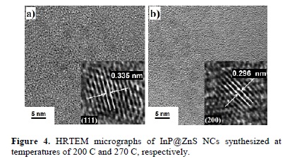
For a closer observation on the crystallinity of the semiconductor nanoparticles and their fine structure, HRTEM images of two samples (synthetized at T = 200 and 270 C) were recorded. From the HRTEM images shown in Figure 4, we can observe the formation of welldefined crystalline nanoparticles for both samples. The lattice spacing in the nanoparticles is clearly visible in the amplified images of the selected areas presented as insets. Interplanar spacing calculated for both samples corresponds well with the interplanar spacing of the corresponding indium phosphide structures of the zincblende phase. We tried to analyze each discrete particle to try to observe the possible presence of ZnS nanoparticles; however, it was not possible to confirm the presence of ZnS on the surfaces of the InP QD's from their HRTEM images, which possibly means that the shell is too thin to be detected. To confirm the formation of the shell-ZnS structure on core-InP, we measured the PL spectra of the colloidal dispersions of semiconductor nanoparticles.
The PL spectra of semiconductor colloids prepared at different temperatures are shown in Figure 5. In this figure we show the PL spectra for samples S1, S2, S3 and S4. It can be observed that for sample S1 there is a broad emission band centered at high energies around 3.07 eV. For sample S2, the band at 3.07 eV decreases its intensity as it is comparable to the 2.5 eV-PL band. For samples S3 and S4 the 3.07 eV-band has almost disappear, and the PL spectra is dominated by the PL band peaked at around 2.4 2.5 eV with a very high increase in the PL intensity. The band at 3.07 eV comes from radiative transitions involving surface states located at the nanoparticles surface; as the temperature of growth increases, there is an increase in the ZnS coverage of the InP NCs, passivating their surface and increasing the intensity of the PL coming from the InP NCs. This effect of passivation has also been observed when CdSe NCs are passivated with ZnS [35].
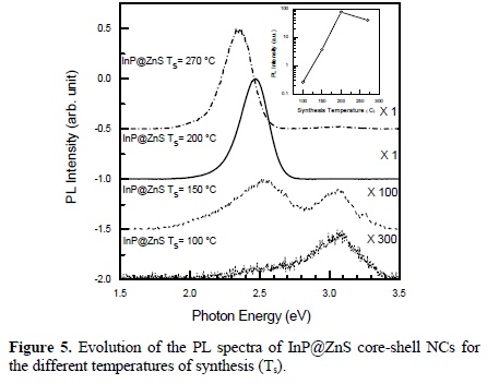
The insert shows the temperature dependence of the PL intensity.
The decomposition temperature of pure DDT is 350 C. In the presence of the other compounds within the reaction mixture, we observed that DDT already begins to react at around 200 C, releasing sulfur for the formation of the ZnS shell. The emission efficiency increases significantly with increasing temperature of synthesis, due to the successful surface passivation of the cores with ZnS shells of wider band gap energy. We attribute the in situ formation of the core/shell structure, to the difference in reactivity of the InP and ZnS precursors applied together. On increasing the temperature of synthesis, the PL emission spectra of the InP/ZnS core/shell NCs presented in this study were redshifted by around 187 meV. The position of the peak shifted towards longer wavelengths suggests an increase in the size of the nanocrystals. This is consistent with TEM and optical absorption results as can be observed in Table 1. As the reaction temperature is increased above 270 C, the diffusion of atoms of In, P, Zn and S at the interface is highly enhanced and the intensity of the PL decreases because there is an increase in the surface states density at the QD/shell interface.
4. Conclusions
The PL emission efficiency of ZnS@InP NCs increases significantly with increasing the synthesis temperature. We attribute the in situ formation of the core/shell structure to the difference in reactivity of the InP and ZnS precursors applied together. Also, we have shown that the InP particle size increases as the temperature of synthesis does. We believe that this remarkable enhancement in optical properties is due to the successful surface passivation of the InP cores with ZnS shells of wider band gap energy. The ZnS shells structurally passivate the dangling bonds on the surface of the cores and also energetically suppress the leakage of excitons from the cores into the shell because of its wider band gap energy as compared to that of the core.
References
[1]. R.M. Iost, J.M. Madurro, A.G. Brito-Madurro, I.L. Nantes, L. Caseli, F.N. Crespilho, Int. J. Electrochem. Sci. 6, 2965 (2011). [ Links ]
[2]. D.V. Talapin, A.L. Rogach, A. Kornowski, M. Haase, H. Weller, Nano Letters 1, 207 (2001). [ Links ]
[3]. X. Peng, Chem. Eur. J. 8, 334 (2002). [ Links ]
[4]. A.P. Alivisatos, Science 271, 933 (1996). [ Links ]
[5]. J. Ziegler, S. Xu, E. Kucur, F. Meister, M. Batentschuk, F. Gindele, T. Nann, Adv. Mater. 20, 4068 (2008). [ Links ]
[6]. S. Gao, C. Zhang, Y. Liu, H. Su, L. Wei, T. Huang, N. Dellas, S. Shang, S.E. Mohney, J. Wang, J. Xu, Optics Express 19, 5528 (2011). [ Links ]
[7]. G. Shen, P. Chen, Y. Bando, D. Golberg, C. Zhou, Chem. Mater. 20, 6679 (2008). [ Links ]
[8]. P. Holmström, L. Thylén and A. Bratkovsky, Appl. Phys. Lett. 97, 073110 (2010). [ Links ]
[9]. C.A. Cattley, A. Stavrinadis, R. Beal, J. Moghal, A.G. Cook, P.S. Grant, J.M. Smith, H. Assender, A.A.R. Watt, Chem. Commun. 46, 2802 (2010). [ Links ]
[10]. U.T.D. Thuy, P.S. Toan, T.T.K. Chi, D.D. Khang, N.Q. Liem, Adv. Nat. Sci: Nanosci. Nanotechnol 1, 045009 (2010). [ Links ]
[11]. P. Reiss, J. Bleuse, A. Pron, Nano Letters 2, 781 (2002). [ Links ]
[12]. J.M. Bruchez, M. Moronne, P. Gin, S. Weiss, A.P. Alivisatos, Science 281, 2013 (1998). [ Links ]
[13].X. Michalet, F.F. Pinaud, L.A. Bentolila, J.M. Tsay, S. Doose, J.J. Li, G. Sundaresan, A.M. Wu, S.S. Gambhir, S. Weiss, Science 307, 538 (2005). [ Links ]
[14]. S. Kim, Y.T. Lim, E.G. Soltesz, A.M. De Grand, J. Lee, A. Nakayama, J.A. Parker, T. Mihaljevic, R.G. Laurence, D.M. Dor, L.H. Cohn, M.G. Bawendi, Nature Biotechnology 22, 93 (2004). [ Links ]
[15]. O.I. Micic, J.R. Sprague, C.J. Curtis, K.M. Jones, J.L. Machol, A.J. Nozik, H. Giessen, B. Fluegel, G. Mohs, N. Peyghambarian, J. Phys. Chem. 99, 7754 (1995). [ Links ]
[16]. Y. Wang, J. Lu, Z. Tong, B. Li, L. Zhou, Bull. Chem. Soc. Ethiop. 25, 393 (2011). [ Links ]
[17]. L. Li, P. Reiss, J. Am. Chem. Soc. 130, 11588 (2008). [ Links ]
[18]. R. Xie, D. Battaglia, X. Peng, J. Am. Chem. Soc.129, 15432 (2007). [ Links ]
[19]. J.R. Heath, J.J. Shiang, Chem. Soc. Rev. 27, 65 (1998). [ Links ]
[20]. W. Xu, Y. Wang, R. Xu, S. Liang, G. Zhang, D. Yin, J. Mater Sci. 42, 6942 (2007). [ Links ]
[21]. Celso de M. Donegá, P. Liljeroth, D.A.M. Vanmaekelbergh, Small 1, 1152 (2005). [ Links ]
[22].U.T.D. Thuy, T.T.T. Huyen, N.Q. Liem, P. Reiss, Mater. Chem. Phys. 112, 1120 (2008). [ Links ]
[23]. L. Li, M. Protière, P. Reiss, Chem. Mater. 20, 2621 (2008). [ Links ]
[24]. B. Koppenhoefer, K. Hintzer, R. Weber, V. Schurig. Angew, Chem. Int. Ed. Engl. 19, 471 (1980). [ Links ]
[25]. S. Xu, S. Kumar, T. Nann. J. Am. Chem. Soc. 128, 1054 (2006). [ Links ]
[26]. D.W. Lucey, D.J. MacRae, M. Furis, Y. Sahoo, A.N. Cartwright, P.N. Prasad, Chem. Mater. 17, 3754 (2005). [ Links ]
[27]. D.V. Talapin, N. Gaponik, H. Borchert, A.L. Rogach, M. Haase, H. Weller, J. Phys. Chem. B 106, 12659 (2002). [ Links ]
[28]. R. Xie, D. Battaglia, X. Peng. J. Am. Chem. Soc. 129, 15432 (2007). [ Links ]
[29]. O.I. Micic, S.P. Ahrenkiel, AJ. Nozik, Appl. Phys. Lett., 78, 4022 (2001). [ Links ]
[30]. L. Li, P. Reiss, J. Am. Chem. Soc. 130, 11588 (2008). [ Links ]
[31]. S.A. Ivanov, A. Piryatinski, J. Nanda, S. Tretiak, K.R. Zavadil, W.O. Wallace, D. Werder, V.I. Klimov, J. Am. Chem. Soc. 129, 11708 (2007). [ Links ]
[32]. L.C. Hernandez, L. Ponce, E. Rodriguez, A. Fundora, G. Santana, J.L. Menchaca, E. Pérez-Tijerina, Nanoscale Research Letters 7, 80 (2012). [ Links ]
[33]. B. Barman, K.C. Sarma, Chalcogenide Letters. 8, 171 (2011). [ Links ]
[34]. B. R. Bennett, R.A. Soref, J.A. del Alamo, IEEE Journal of Quantum Electronics 26, 113 (1990). [ Links ]
[35]. L.G. Vega Macotela, J. Douda, T.V. Torchynska, R. Pena Sierra, L. Shcherbyna, Phys. Status Solidi (c) 7, 724. (2010). [ Links ]

