


 nueva página del texto (beta)
 Inglés (pdf)
 Artículo en XML
 Referencias del artículo
 Enviar artículo por email
 Citado por SciELO
  Similares en
SciELO
Similares en
SciELO 
 Permalink
Introduction
The plasma is known as the fourth state matter, it is an ionized gas containing electric charge particles (radicals, ions, electrons, neutral atoms, molecules and other exciting species in a concentration relationship which global total electric discharge equals to zero), which maintain collective energetic interactions simultaneously. These interactions make the plasma highly reactive and can be used in wide applications through processing its control parameters. Commonly, according to its temperature, the plasma is classified into two main groups: cold plasma and thermal plasma (Tendero et al., 2006; Hnautic et al., 2012).
For cold plasma, the ions and neutrons temperature is near to environmental temperature and it is usually produced at low pressure (less than 1 atm) (Schutze et al., 1998).
In recent years, the cold plasma has been widely used for chemical processing of water treatment, material manufacturing, semiconductor devices production, industrial disinfection, etc. The plasma generator purpose is to provide ionized species for deposition, removal, and surface preparation in the manufacturing process. The predictable, repeatable and ions characteristics are critical for the end product quality (Millner 2008; Kim et al., 2006; Ren et al., 2016).
There are several excitation forms to obtain cold plasma as microwave or radiofrequency systems, where operation frequency is too high and the equipment requires complex vacuum features (Wang et al., 2017). Another method is by using electrical fields generated through direct current, alternating current or pulsed discharges. Intense electrical fields promote gas electrical rupture; the particles are charged and accelerated on this field, causing a partially ionized gas due to elastic collisions of these particles. The electrical fields can be produced at high voltage and high frequency (Birle et al., 2011; Levchenko et al., 2016).
An alternative to producing that features of electrical fields described above is by electric inverters, which are electronic circuits that produce alternant current from direct current with frequency and voltage control. Some applications of electric inverters are for supplying, electric arc discharge or variable speed AC motor driving (Martínez et al., 2014).
The aim of this work is to obtain cold plasma at atmospheric pressure and vacuum by using a high-voltage and high-frequency power electronic source in different reactors types such as jet system, dielectric barrier system, and double dielectric barrier system. The inverter objectives are to control voltage discharge, pulsated discharge time, and operation frequency for optimizing plasma generation.
The rest of the paper is organized as follows: section II presents the power electronics source development and general considerations. On section III, numerical results, experimental results, and plasma discharges on three different plasma reactors are presented. Finally, section IV concludes the paper.
Power electronics source development
In this section, the high voltage and high-frequency power electronics source design for non-thermal plasma is present. For this purpose, a full bridge inverter modulated by PWM is considered, as shown in Figure 1.

The general idea is to provide an AC voltage signal at high frequency and high voltage to generate an electric field, in order to make the discharge on two electrodes connected at the transformer output an obtain the non- thermal plasma. There are not exists an operation power desired each plasma reactor unique characteristics where the power applied depends on operation pressure, working gas, among others. In the literature are found a power up to 200 W or 400 W at high frequencies (Schutze et al., 1998). According to the previous research, the power source is designed to operate in a wide range of powers, from 0-600 W, this allows to have control in different applications, and possibilities to use it in different plasma reactors. To achieve these characteristics, the maximum power is fixed at 600 W, and the current at 0.6 A, then the voltage is obtained by
The design considers a boost transformer of 1:50 relation spin, then, the value provided for the input DC source it must be at least 20 V.
The topology considered for generating the AC signal is formed by four switching semiconductor devices (M1, M2, M3, M4). These devices are capable to provide positive, negative, and zero voltage to the load, by turning on and turning off as seen in Table 1.
Table 1: Voltages levels by turning on and off the switching devices
| VCD | M1 | M2 | M3 | M4 |
| +VCD | On | Off | On | Off |
| -VCD | Off | On | Off | On |
| 0 | Off | Off | Off | Off |
The output current depends on the load coupled to the inverter, the transformer primary side is considered as RLC series load, which generates a quasi-sinusoidal signal. The inverter is working as a resonant inverter, where the resonant frequency (Karys, 2009) is given by
And the quality factor (Juárez et al., 2016) is obtained using the following equation
Finally, the voltage and current at the end of the transformer feed the plasma reactor, in order to provide enough energy for the plasma discharge.
Inverter construction stage
Three blocks are primordial on inverter construction stage, as described in the following paragraphs.
A) Power block
The power block shown in Figure 2 in the red box is the system heart, generates a square bipolar signal from a DC signal provided by the source. It consists of an H-bridge with four transistors and a DC source. The transistors are selected according to the nominal power (0-600 W) and the commutation frequency (0-150 kHz), so then, the MOSFET IRFP4550 is suitable for these characteristics. The DC source is given by a programmable commercial source BK PRECISION XLN10014, capable to vary its output voltage from 0 to 100 V on DC and 14.4 A. This allows to achieve the power stated on Section II.
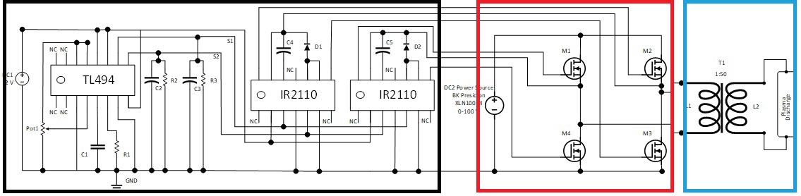
In order to activate the power devices, it is necessary to add a circuit, to guarantee the correct voltage level from the control block, this can be achieved using a driver. This driver has three purposes: providing high impedance at the input, adapt the voltage levels, and incorporate a dead time. The selected device was the IR2110, capable to control 2 MOSFETs of the same branch. The IR2110 electric diagram the H-bridge is depicted in Figure 2 in the black box. The capacitor and resistor values are given in the datasheet, the S1 and S2 signals are obtained from TL494.
B) Control block
The control block, create the signals to achieve the activation and deactivation of the power semiconductor devices, this can be accomplished by a square signal oscillator. The device selected consist in a TL494, capable to provide two pulse width modulation (PWM) signals at fixed or variable frequency. The TL494 compares a saw-tooth signal with a constant given by an internal capacitor to attain the width desired at the PWM signal, to obtain the control signals.
The TL494 is also capable to generate a dead time, consisting of a small delay at the transistor when turning on. The dead time is used to prevent short circuits, due to the MOSFETs have to work in pairs (branch) according to the electric diagram (basic inverter performance).
The frequency of the oscillator at TL494 is programmed by selecting timing components R1 and C1. The TL494 internal oscillator charges the external timing capacitor with a constant current, the value of which is determined by the external timing resistor. This produces a linear-ramp voltage waveform. When the voltage across capacitor reaches 3 V, the oscillator circuit discharges it and the charging cycle is reinitiated. This oscillator frequency is equal to the TL494 output frequency. For push-pull applications the output frequency is given according to the component datasheet by
Where C1 is fixed to 0.0001 µF and for R1 a precision potentiometer of 0-100kΩ is used. Hence, f 0 the output frequency range goes from 5 to 150 kHz. The push-pull configuration allows to habilitate alternatively each output then output 1 goes to transistors M1 and M2 from Figure 1, and output 2 to transistors M3 and M4. The maximum duty cycle for each signal S1 and S2 is 47 %, 3 % of each signal is the dead time, this is given by the potentiometer Pot1 in Figure 2 in the black box. The greatest energy transference from BK Precision source to the power block and finally to the plasma occurs at a maximum duty cycle, if this duty cycle reduces, can generate a weakly ionized plasma, unstable, and without enough energy to light it. The electric diagram of the control block is given in Figure 2 in the black box. Capacitors and resistors values are obtained from the datasheet component. Besides, the source DC1 is a commercial source BK PRECISION 9104 which operates from 0-10 V and 0-10 A. It is fixed to 12 V, and the objective of this source is to provide energy to the control block and the drivers IR2110.
C) Transformation block
This block leads the AC signal coming from the power block to the level required for supply the load. For this purpose, a step up transformer is used, capable to manage the power of 1 kW and the spin relationship of 1:50, this is shown in the ideal form in Figure 2 at the blue box. The resistance and capacitance values at the primary of the transformer are physically measured using a BK PRECISION Bench LCR/ESR 889B from the step-up transformer, in order to obtain more accurate results. The resistance, inductance, and capacitance on the transformer primary side are 0.470 Ω, 37.9 µH and 150nF respectively. These values are used on equations (2) and (3), to obtain the series H-Bridge resonant circuit parameters, with a quality factor of 33.81 and a resonant frequency of 66.75 kHz. The block diagram of the proposed prototype is depicted in Figure 3.

Power electronics source results
A) Simulation results
In order to validate the proposed circuit, the numerical simulation of the power electronics source using Pspice 8.0 was carried out. The DC voltage is fixed at 30 V, the commutation signals have a 65 kHz frequency, as the load on the transformer secondary side a 50 kΩ resistor is used only to verify the system performance. Figure 4 shows the simulated circuit. The circuits at the bottom of the figure simulate the PWM obtained from TL494 circuit, due to, the Pspice does not have the libraries for the TL494 and the drivers IR2110. In the transformer, the parasite values (obtained with a BK PRECISION Bench LCR/ESR 889B) are included for having more accurate results. The R3 resistor simulates an isolated ground given by transformer isolation, due to its high value does not affect the simulation.

Then, in Figure 5, the output voltage and output current at the transformer primary is depicted. The square signal represents the voltage (black color) and the quasi-sinusoidal the current signal (blue color).

The square signal corresponds to the inverter output, obtaining -30 V to 30 V, and the current is quasi-sinusoidal and has different phase because of the load. The current has a different scale, its real value is of 0.7 A, it presents at the same graphic to appreciate the output waveforms.
Afterward, the voltage on the load and inverter output voltage is shown in Figure 6. The square signal corresponds to the transformer primary signal (black color) and the quasi-sinusoidal signal to the transformer secondary (blue color).

The results obtained prove the correct performance of the power supply, giving the desired power, enough to generate plasma. The signal before passing the transformer is a square signal of -30 V to 30 V at 65 kHz, and after the transformer, the signal becomes quasi-sinusoidal of 1.3 kV, due to the parasites values.
B) Power source construction
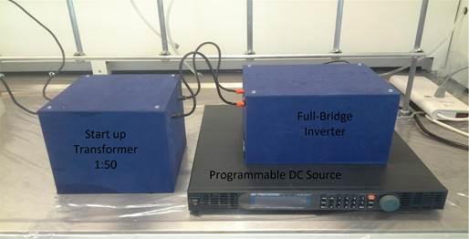
The power electronics source was built following the characteristics described in section two of this document. Figure 7 shows the full-bridge inverter prototype, corresponding to the power block and the control block.

Then, Figure 8 depicts the experimental setup, with the DC source and the elevator transformer connected to the full-bridge inverter.
C) Experimental results
The experimental setup previously described was configured with the next values: the DC source was fixed at 40 V, and the switching frequency at 65 kHz. The voltage output and the current output at the primary of the transformer are shown in Figure 9. The current is the quasi-sinusoidal signal and the voltage corresponds to a square signal.

The results are consisting according to the Figure 4, the inverter has a square output of -40 to 40 V and the current is quasi-sinusoidal of 0.6 A of amplitude due to the load and have a different phase.
Then, Figure 10 depicts the voltage at the inverter output as a square signal and the output voltage at the secondary as a sinusoidal signal, with a high voltage and high frequency. These results are consistent with the simulation results in waveform and amplitude. This guarantee enough energy power to realize the plasma discharge.
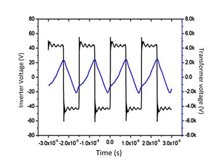
A comparative table is shown in Table 2, to present the coherency between the results obtained by simulation and experimental results, the inverter output voltage is multiplied by a factor of 50 due to the transformer.
D) Plasma discharges
For proving the power electronic source in plasma generation, different plasma reactor configurations were carried out, where the equipment was inside a cabinet built with isolate material. Besides, the circuits have a ground connection for electric discharge. The user has to wear glasses, industrial boots, and dielectric gloves for high voltage.
D.1) Dielectric barrier discharge
Among atmospheric pressure plasma produced in several ways, the dielectric barrier discharge is mainly characterized by the use of one or more dielectrics disposed between the electrodes. This configuration produces random multifilament micro-discharges. A high-frequency electric field is required for this purposes. The dielectric barrier distributes the micro discharge uniformly throughout the discharge volume, generating energetic electrons that create other active species (Jiang et al., 2018; Li et al., 2018). The diagram is depicted in Figure 11.

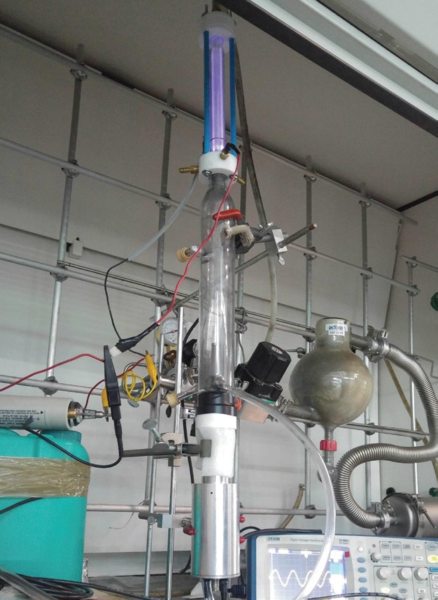
Using the experimental setup described above, coupled with the proposed configuration, and Helium as plasma gas, the discharge showed in Figure 12, is obtained.
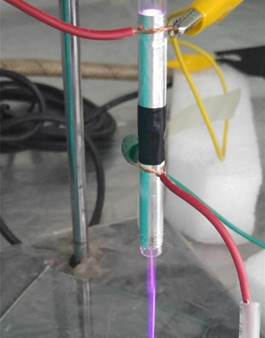
The dielectric used was a 20 cm long inert quartz circular tube, with 1.5 cm of diameter with two aluminum electrodes of 3 cm length and gap of 2 cm, the helium provided was regulated using a needle valve. The dielectric barrier discharges applications are well known as etching, cleaning, thin films deposition, plasma polymerization, surface treatment, materials functionalization, and modification, etc.
D.2) Doubles dielectric barrier discharge
The double DBD plasma is provided through a double cylindrical dielectric barrier. This arrangement is useful to prevent arcing between the (inner) powered electrode and a plasma exposed sample which is particularly unwanted for general applications (Florian et al., 2015; Zhang et al., 2018). The Double dielectric reactor diagram is shown in Figure 13 the purple color indicates the plasma generated.

Then, Figure 14 shows a superior view of de Double dielectric reactor diagram, for better understanding of the configuration. The orange color denotes the ground electrode, the gray color the two dielectric barriers, and the black color the high voltage electrode.
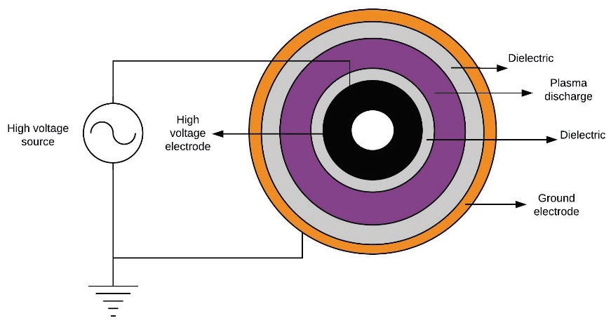
The double barrier dielectric reactor operation was created, on the coaxial configuration with quartz walls with central and external electrodes. The discharges are operating in a 5 kHz to 150 kHz range, so the operating frequency was settled at 65 kHz (resonant frequency). The plasma gas was helium. Figure 15, shows the double dielectric discharge ionizing helium using the prototype developed. Dielectric material presence between both electrodes requires high AC voltages applied in a 1.2 kVp to 12 kVp, and currents from 20 to 100 mA. The power applied goes from 200 W to 1.2 kW.
D.3) Jet discharge
One of the cold atmospheric plasma sources is jet type, which can generate plasmas in open space rather than in confined discharge gaps and it is characterized by flexibility, compactness, and efficiency (Fan et al., 2012). The Jet plasma reactor diagram is depicted in Figure 16.
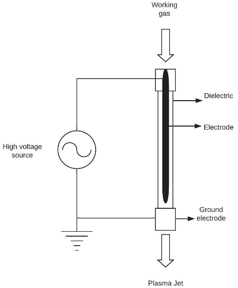
In order to produce discharges without electric arcs, a jet plasma reactor was built, for high voltage discharges at 15 kVp and operation frequencies for 5 to 150 kHz. On jet plasma discharge a shining on the reactor extreme is produced. This shining is used for material treatment and modifying the material structure. The plasma generation was configured under parameters shown in Table 3.
Table 3: Jet reactor parameters
| Voltage | 15 kVp |
| Current | 20 mA |
| Power | 300 W |
| Plasma global temperature | < 70 °C |
| Plasma gas | Air |
| Air flux | 6 LPM |
With the parameters stated above, the plasma discharge obtained on a jet type reactor is shown in Figure 17, at atmospheric pressure.

Conclusions
The power electronic source developed allow varying the operating frequency from 5 kHz to 150 kHz, and a duty cycle from 0 to 47 %. It is coupled to a BK PRECISION XLN10014 programmable DC source, and a general purpose star up transformer to provide until 15 kVp at 1.4 kW of power. The variable frequency allows to syntonizer the natural resonance zone, and it is important because the regions of maximum voltage amplification aids to ignite and generate stable plasma discharges.
The experimental prototype design was first tested by numerical simulations and then it was built physically, the results in both, simulation and physical are consistent and coherent.
The designed prototype is useful to generate plasma discharges, which can help to modify materials, in order to enhance electrical, mechanical, and thermal properties. The proposed prototype has an electronic control that allows varying some parameters like frequency, and duty cycle, this are some advantages against plasma generation through radiofrequency, and microwave.
Plasma discharges were made for ionizing helium on two different reactor configurations: dielectric barrier, double dielectric barrier, and ionizing air on a jet type reactor. In all of them, it was possible to achieve an electrical field strong enough to reach the breakdown voltage and generate plasma discharge.
The system advantage presented in this work against other high voltage source for plasma generation, is the versatility to generate plasma at vacuum and atmosphere pressure, with electrodes on direct contact to the plasma or through dielectric discharges.
As future work is proposed to implement a feedback nonlinear control as sliding mode control or fuzzy control, to improve the prototype features, the system is in open loop, and also taste the plasma generated to modify materials.

