


 nueva página del texto (beta)
 Inglés (pdf)
 Artículo en XML
 Referencias del artículo
 Enviar artículo por email
 Citado por SciELO
  Similares en
SciELO
Similares en
SciELO 
 Permalink
Introduction
After its emergence in the the 90th by Meynard and Foch, applications of the Flying Capacitor Multicell Inverters (FCMI) has been continuously growing, leading to a wide study in the different areas of the knowledge (Meynard et al., 2002). A considerable amount of literature has been published concerning about this kind of static power converter topology on industrial applications, for instance: STATCOM™ transport trains active filters to eliminate total harmonic distortion THD, cd to cd and cd to ca power converters, and more recently in Eolic conversion energy (Rodriguez et al., 2012; Abu et al., 2010; Fernao et al., 2012).
Precedent studies about a Three Cell Flying Capacitor Inverter in half-bridge, coupled in an electrical model of a Dielectric Barrier Discharge (DBD) are presented by (Flores et al., 2009). A simulation of the electrical model is used in order to estimate the experimental results at different gas discharges, and operation frequency about 12.5 and 47 kHz implementing different commutation strategies. Nevertheless, these simulations results are limited to half-bridge and three cells. Previous works of the FCMI show a full-bridge configuration applied as electrical source in DBD applications operating at 10-20 kHz (López et al., 2015) and 12.5-50 kHz (Péña et al., 2017). In these works, experimental and simulation results show an agreement application implementing this kind of multicell inverter topology operating at high frequency.
From the perspective of FCMI technology design, switching coupling, command signal generator system and high frequency semiconductor drivers, are the considerable disadvantages, not only because specialized components are required, but also power losses and technological limitations. In fact, this kind of power inverter is usually implemented at low frequency (Zhe et al., 2009; Rodriguez et al., 2012; Tolbert et al., 2000; Samir et al., 2010).
Multicell Converters were developed in order to satisfy the electrical characteristics of high voltage and current, by Voltage Source Inverter or Current Source Inverter respectively, and more recently the high frequency operation in the order of hundreds and thousands of Hertz. In addition, the operation frequency in the FCMI is given by f 0 = N∙ f SW, where f SW is the commutation frequency; the same that semiconductor devices operation, and N is the number of cells configured like one leg in the FCMI structure. That property bringforward an intrinsic characteristic not commonly used in the typical static converters, so f 0 is proportionally N times than f SW and that statement is an advantage, taking in account that semiconductor devices, like Thyristors, GTOs and power BJTs operates at low frequency in the order of some kilo-Hertz at tens to hundreds volts-amperes. In counterpart, MOSFET and IGBT devices operates about tens to hundreds of kilo-Hertz at some tens volts-amperes (Hirofumi, 2009). That characteristics voltage-current and frequency is a restriction to choose the semiconductor device, because the more voltage and current is needed the frequency interval of work is reduced and vice versa (Loren, 2003). In the other hand, that statement is solved by using the FCMI. First, its main property consists in distribute the total voltage (VSI) or current (CSI) in the total number of cells N and when the FCMI operates at Fundamental Frequency (F-F) strategy the output operation frequency f 0 is given by f 0 = N∙ f SW, where f SW is the switching frequency equal to the F-F. So, both characteristics are used in order to overcome the above-mentioned disadvantages.
Moreover, until few decades ago the main disadvantage of the FCMI is their complexity: they require a great number of power devices and a rather complex command firing-circuit made by analog-digital circuits. However, the current technology based on micro-controllers, Digital Signal Processor (DSP), Field Program Gate Array (FPGA), and other technologies like Arduino® or Raspberry™ has allowed the higher processing capacity in the control design with any technique implemented such as; Simple Square Wave (SSW) or Fundamental Frequency (F-F) and Pulse Wide Modulation (PWM) commonly implemented in the strategy control for FCMI (Holmes and Lipo, 2003; Rodriguez et al., 2002). The advantage to implement PWM topologies is the reducing of the Total Harmonic Distortion (THD) but as consequence, large protection circuits (dv/dt or di/dt) are required in order to help the commutation semiconductors, and so the losses increase (Aguillón et al., 2004).
Considering the above mentioned characteristics about control implementation, the proposed FB-FCMI implements an F-F strategy and as a result of the command firing-signals it produces a typical square waveform output u 0 at frequency f 0 = N∙ f SW, moreover due to f SW is N times lesser than f 0, hence the commutation losses decrease. Actually, that property is not commonly applied on this kind of static converters, but nevertheless, on this work this feature is improved not only in order to reduce the switching frequency and complexity of the command signals implementation, but also the goal of the RLC circuit series with the FB-FCMI achieves a resonant operation.
As a contribution to operate the FB-FCMI in resonant mode converter, the design and simulation results are shown. The calculus of either, L 0 and C 0 resonant elements, is presented. Finally, the high voltage application is presented by implementing an electrical model of one dielectric barrier discharge (DBD). The simulation results show the implementation of the FBFCMI operating at 20 kHz in resonant mode in order to drive a dielectric barrier discharge in helium.
Simulation design
Full-bridge Flying Capacitor Multicell Inverter topology
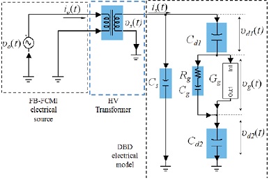
A resonant FB-FCMI coupled to DBD electrical model is shown in Figure 1. The inverter is constituted by six commutation cells (three upper-leg and three lowerleg), each cell is composed by two complementary MOSFET [M1, M1’], [M2, M2’], [M3, M3’], [M4, M4’], [M5, M5’] and [M6, M6’] every one with its antiparallel diode, there is a flying capacitor C p , where p is the position of cell in upper-leg and C p ’ in lower-leg.
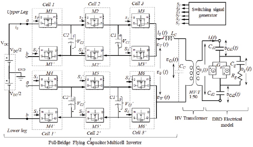
The flying capacitor voltages V C1 =V C1 ´ and V C2 =V C2 ´ are defined by; V Cp, Cp´ =(𝜌/N) ⋅ V DC where p is the position of the cell in the structure and N is the number of total cells. Also, the blocking voltage in the MOSFETs is estimated by V MN, MN´ =(V DC /N) and the average current is; I kavg =T on / T∙I S where T on is the turn-on period, T is the total period and I S is the supply current (Meynard et al., 2002).
The operation of FB-FCMI is achieving an equal distribution of the total voltage in the blocking-state MOSFET. This occurs when flying-capacitors are charged at; V C1,C1´ = V DC / 3 and V C2,C2´ = 2V DC / 3, considering as ideal voltage source. The accurate MOSFET firing commutation pulses involves that C1=C1´ and C2=C2´, and that condition guarantees the appropriate voltage, and as result; the output voltage u 0(t) operating at output frequency f 0 = 3⋅ f sw or T 0 = T sw /3. Figure 2 shows tree representative commutation pulses [S 1 , S 2 , S 3 ] provided to MOSFET M1, M2 and M3, signals are in phase shift 120° and 240° respectively, the main voltages are presented like; output υ0 (t), referenced to upper-leg υ W (t) and lower-leg υ V (t). So, because of the voltage difference between υ W (t) and υ V (t) is made by υ0 (t).

The resonant RLC series coupled to FB-FCMI
As Figure 1 shows, a Dielectric Barrier Discharge electrical model is coupled to FB-FCMI. Then, the equivalent circuit can be considering by a resonant RLC series circuit. Figure 3 shows a resonant RLC series circuit determinate by the inductance L C primary winding of high voltage transformer and the secondary winding capacitance presented in the primary one as C C . The analysis of L C -C C values is presented in order to get the resonant operation of the FB-FCMI.

The RLC series circuit of the Figure 3 is supplied by the voltage υ0(t). Then, the total impedance Z T obtained in frequency domain is given by
where ω = 2πf is the angular frequency and f is the linear frequency output f 0. The total impedance for the n th frequency component
Then, the magnitude and angle impedance values for the n th harmonic are defined as
Also, the voltage u 0(t) is a square signal provided by the FB-FCMI at the resonant RLC series circuit in Fourier term
where V m =V DC /3 is the maximum amplitude to the output square voltage, considering only the n odd values. So, using Ohm law to obtain the output current i 0(t) based on (2) and (5) then
In an ideal resonant RLC series circuit the i 0(t) flow from R to L without losses, but the capacitor voltage is in phase shifting -π/2 radian, therefore the capacitor voltage u C (t) is
Then, the total voltage gain A u =u C (t)/u 0(t) and angle, considering the n th harmonic is
Finally, the transfer function magnitude
where ω 0 2 = 1/LC y Q = 1/ωCR
By means (9) and (10) is possible to know the magnitude
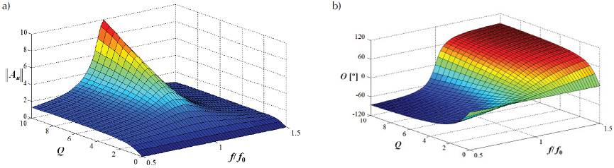
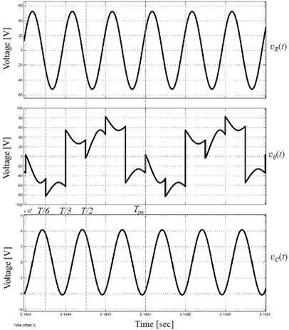
Figure 5 shows the simulation results of the FB-FCMI obtained with SIMULINK/MATLAB®, the voltage υ R (t)and current i 0(t) values are in the same angle phase ϕ=0 at f/f 0 condition. Otherwise, Figure 6 shows the voltages in υ R (t), υ C (t) and υ0(t) at resonant condition, the waveforms evidence the statement f 0=3·f sw ; because the output frequency in R or C passive electrical components is f 0≈20 kHz, three times more than commutation frequency f sw ≈6.66 kHz in the voltage υ0(t).

The increasing of the output frequency f 0 is a natural property and benefit of the FB-FCMI when it operates at Fundamental Frequency, so not only is an advantage in order to increases the frequency N times but also overcomes the disadvantage of commutation losses at frequency f sw . Thus, the MOSFET devices operate at f sw the commutation losses are reduced, and as consequence snubber circuit protection versus voltage dv/dt and current di/dt are diminished.
Figure 7a shows the voltage V MN (t) and current I MN (t) through the MOSFET at Zero-Current Switching. The ZCS is when the current through a switch is reduced to significantly zero amperes prior to when the switch is being turned either on or off. It is due to RLC resonant circuit operation. Therefore, the advantage is the considerably reduction of power dissipation in the MOSFETs. Figure 7b shows the simulation results on instantaneous power P i (t) and P RMS in semiconductors, the RMS value is ~7 mW.

The FB-FCMI at resonant mode: Simulation set-up
The FB-FMCI showed in Figure 1 is developed and running on SIMULINK/MATLAB® using the SimPowerSystem libraries. In order to get the best performance a previous calculus of RLC resonant components either SimPowerSystem or Funtional-Block was made to achieve the best tuning of the resonant condition. The parameter simulation values are; f= 20 kHz, C=10 nF, L=6.333 mH, R = 1Ω and V M =66 V. The simulation parameters on [C1, C1’] and [C2, C2’] are VDC=200 V, V C1 =V C1 ’= 133.33 V and V C2 =V C2 ’=66.66 V also the voltage response of flying capacitors are shown in Figure 8a, from this; it is possible to sustain the correct values in open-loop control. Hence, the static inverter gets its natural balance as Meynard and Foch describes in (Meynard et al., 2002). Figure 8b show a detail of voltage V C2 (t) and i C2 (t) current in flying capacitor named C2 working as resonant mode, the ripple voltage ∆v C2 (t) is about 3.75% of the total voltage V C2 (t) and ∆i C2 (t)≅2.5Ap-p, even though the average current throughout C2 estimated by means Origin® is about zero. Then, both C1 and C2 work like an ideal voltage source.
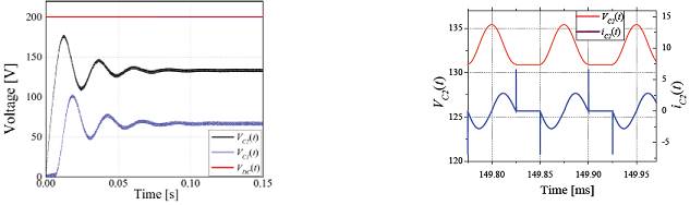
Figure 8 a) Flying Capacitors voltage response V C1 (t) and V C2 (t), b) Detail of voltage V C2 (t) and current i C2 (t) at resonant mode
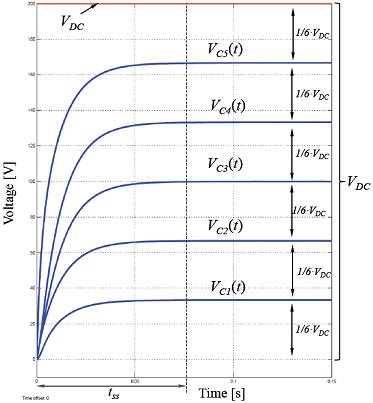
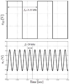
Simulation set-up of a six cell FB-FCMI was designed based on theory of experimental section. Figure 9 shows the voltage in flying capacitors; V C5 (t)=5/6·V DC´ V C4 (t)=4/6 · V DC´ V C3 (t)=3/6 · V DC´ V C2 (t)=2/6 · V DC and V C1 (t)=1/6 · V DC considering V DC = 200V. The natural balance in all cases is getting about t ss ~0.075 seconds. Moreover, Figure 10 shows an evolution of capacitor voltage υ C (t) expressed as function of u S3 (t), in these case the output frequency in the element R, is f 0≈20 kHz in so far as the command signal frequency u S3 (t) operates at f sw ≈ 3.333 kHz, therefore the statement f 0 = N · f sw , where N is the number of cell, is substantiated in this work.
The FB-FCMI coupled to high voltage application
The high voltage application consists in a proposed tree-cell FB-FCMI coupled to a high voltage transformer where its primary winding inductor is part of the RLC resonant-circuit and the secondary winding is coupled an equivalent electrical model of Dielectric Barrier Discharge see Figure 1. The DBD model involves a stray capacitance C S due to effect of the capacitance reactor, two dielectric capacitance C d1 and C d2 corresponding to dielectric material as glass, then a parallel circuit is formed; first by a series load R g ‒C g , and second by a current source controlled by voltage V g . Figure 11 shows the schematic and equivalent DBD proposed in (Flores et al., 2009).
The goal of proposed of an electrical model is to provide more information about voltage and current values at the electrical discharge, because in the experimental set-up not only the voltages υ d (t) and υ g (t) are not measurable but also parameters are not well known because there are not conventional methods with measurement instruments. Therefore, after simulation processes in SIMULINK/MATLAB® the voltages and currents in the DBD are shown in Figure 12.
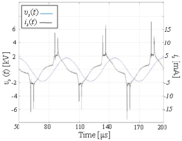
Finally, a simulation of DBD running in helium gas and driven by the resonant tree-cell FB-FCMI, which deliver electric power through primary winding towards DBD coupled in the secondary side. Thereby, Figure 12 shows the electrical behavior of voltage υ s (t) and current i s (t) typically in a DBD taking in account literature information in (Flores et al., 2009) and considering parameters as:
type of ionized gas
applied voltage υ s (t)
current discharge i s (t)
operation frequency 20 kHz
reactor geometry
In the simulation results voltage υ s (t) and current i s (t) are out of phase because DBD load is predominantly capacitive, as shown in the electrical model of Figure 11. This is an intrinsic characteristic of the electrical DBD behavior; however the system is in resonant mode operation, but the total power consumption by electrical discharge is in the order of units of watts and efficiency is ~20% (Flores et al., 2009).
Conclusions
The simulation of a FB-FCMI at resonant mode is presented. The command control generates twelve signals at Fundamental Frequency strategy operating, at f sw =f 0/N, where N is the total number of cells in the static inverter. The statement about relation between output frequency and commutation frequency is given by f o =N·f sw , in this work in order to validate that condition from this kind of power static inverter, not only a three-cell flying capacitor inverter was designed but also a six-cell inverter was simulated. So, the natural balance of the voltage in flying capacitors at open-loop control in both cases is correct achieved. The RLC passive elements are designed based on the resonance frequency which is the same that the output inverter frequency f 0=20 kHz, hence optimal coupling between RLC and FB-FCMI was successfully set-up simulated in MATLAB®. Because of resonant condition, the semiconductor devices operate at ZCS mode properly, so the dv/dt snubber circuit protection is reduced in its size. Finally a full system conformed by FB-FCMI coupled at DBD electrical model is running on SIMULINK/MATLAB® in order to prove the high voltage application to generate electrical discharges in helium gas.

