


Servicios Personalizados
Revista
Articulo
 Inglés (pdf)
 Artículo en XML
 Referencias del artículo
 Enviar artículo por email
Indicadores
-
 Citado por SciELO
 -
 Accesos
Links relacionados
-
 Similares en
SciELO
Similares en
SciELO
Compartir

 Permalink
Ingeniería, investigación y tecnología
versión On-line ISSN 2594-0732versión impresa ISSN 1405-7743
Ing. invest. y tecnol. vol.16 no.2 Ciudad de México abr./jun. 2015
High Efficiency Single-Phase Transformer-less Inverter for Photovoltaic Applications
Inversor monofásico de alta eficiencia sin transformador para aplicaciones fotovoltaicas
Vázquez-Guzmán Gerardo1, Martínez-Rodríguez Pánfilo Raymundo2 y Sosa-Zúñiga José Miguel3
1 Laboratory of Electricity and Power Electronics, ITESI Department of Electronic Engineering, Irapuato, Guanajuato. E-mail: gerardo.vazquez@itesi.edu.mx
2 Laboratory of Electricity and Power Electronics, ITESI Department of Electronic Engineering, Irapuato, Guanajuato. E-mail: pamartinez@itesi.edu.mx
3 Laboratory of Electricity and Power Electronics, ITESI Department of Electronic Engineering, Irapuato, Guanajuato. E-mail: jmsosa@itesi.edu.mx
Received: August 2013,
Accepted: May 2014.
Abstract
Photovoltaic (PV) inverters have a very important role in the energy market, therefore they must possess excellent characteristics regarding cost and reliability. The PV structure most often used in the conversion stage of solar energy system includes a Low Frequency Transformer (LFT) which provides galvanic isolation, but on the other hand reduces the overall efficiency and increases the total size and cost of the system. An alternative to reduce the size of the system and the losses, is to use a High Frequency Transformer (HFT), the problem in this case is that additional power stages must be included in the system. The additional stages increase the power losses in the conversion process, as a consequence the efficiency of the system is reduced. Therefore the tendency is to remove the transformer in order to increase the efficiency and reduce the cost. A security problem regarding common mode currents arise when the LFT or HFT is omitted. In this paper an inverter topology to deal with the problem of the common mode currents is proposed. Numerical results are performed in order to prove the performance of the topology regarding efficiency and Common Mode Voltage (CMV) issues.
Keywords: photovoltaic systems, common mode voltage, leakage current, efficiency, parasitic capacitance.
Resumen
Los inversores fotovoltaicos (FV) tienen un importante rol en el mercado de la energía debido a sus excelentes características en relación con el costo y la confiabilidad. La estructura más usada en la etapa de conversión de un sistema de energía solar incluye un transformador de baja frecuencia (TBF) el cual proporciona aislamiento galvánico, pero por otro lado reduce la eficiencia total e incrementa el tamaño y costo del sistema. Una alternativa para reducir el tamaño del sistema y las pérdidas de potencia es usar un transformador de alta frecuencia (TAF), el problema en este caso es que se deben usar algunas etapas de potencia adicionales. Las etapas adicionales introducen pérdidas de potencia en el proceso de conversión de la energía por lo que la eficiencia del sistema se reduce. Por lo tanto, la tendencia en la implementación de este tipo de equipos es remover el transformador para incrementar la eficiencia y reducir el costo. Sin embargo, cuando no se provee al sistema de aislamiento galvánico, surge un problema de seguridad relacionado con las corrientes parásitas de modo común. En este artículo se propone una topología de inversor para resolver el problema de las corrientes parásitas de modo común en sistemas FV sin transformador. Se proporcionan resultados de simulación con los cuales se hace un análisis relacionado con la eficiencia y el comportamiento del voltaje de modo común (VMC) para validar la topología propuesta.
Descriptores: sistemas fotovoltaicos, voltaje de modo común, corriente de dispersión, eficiencia, capacitancia parásita.
Introduction
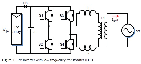
The PV renewable energy has become a very important electrical energy source within the entire energy market. The growing is mainly due to the fact that these systems have been constantly improving in terms of efficiency, power, reliability, etc. On the other hand, the policies stated by the governments in many countries have allowed the spread of the PV systems. The PV system can be designed either in island or grid connected mode being the last one the most commonly used (Kjaer et al., 2005). The grid connection allows injecting the power generated into the electrical grid; in order to achieve this objective, the PV system is commonly set by using three stage: the PV array, the power inverter and the grid filter with the galvanic isolation (Kerekes et al., 2009). In the conventional PV systems, the last stage includes a LFT to link the converter with the electrical grid to provide galvanic isolation as it is shown in Figure 1. However, the main problem with the LFT is that it introduces around 2% of power losses in the system yielding low efficiency. Furthermore, the LFT increases the total cost of the system and the transformer size is big due to the operating frequency that coincides with the frequency of the electrical grid which can be 50 or 60 Hz (Gonzalez et al., 2007).
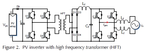
In order to solve the problem of the transformer size, a HFT has been proposed as intermediate stage (Li & Wolfs, 2008; Xue et al., 2004), the system is shown in Figure 2. However, the efficiency in this case is significantly reduced, not only because of the losses in the transformer but also because of the additional power stages that must be added in the power conversion process. Since the efficiency is one of the most important issues in a PV system, transformerless inverters have emerged to mitigate the problems of the galvanic isolated systems. As the transformerless inverters are connected directly to the electrical grid, there is not galvanic isolation between the PV system and the electrical grid dealing in new problems to be solved.
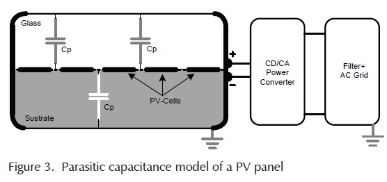
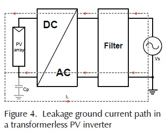
A PV solar panel naturally presents a stray capacitance which is formed between the PV cells and the grounded frame like in Figure 3. Thus, when the PV generator is connected to the grid by means of a transformerless inverter, a leakage current can flow through the stray capacitances as it is shown in Figure 4. Then, the leakage current can generate additional power losses in the system and a high risk of electrical shock for the users in contact with the PV installation (Gubía et al., 2007). On the other hand, a resonant circuit is formed between the parasitic capacitances, the impedance of the ground path and the passive elements in the output filter of the converter (Salm et al., 2012; Yang et al., 2012). The resonance peak can reach high values yielding serious problems in the operation of the circuit. Unfortunately, the value of the stray capacitance depends on operational and whether conditions a: humidity, PV panel surface, the material used in the metallic frame and the values in the passive elements of the power converter (Kerekes et al., 2007, Ji et al., 2013; Hou et al., 2013), therefore, it is not possible to precisely determine its value. Nevertheless, some experiments have been done in order to estimate the value of these capacitances which according to Lopez et al. (2010) is between 50-150 nF/Kw, which is enough to conduct current to the ground at the switching frequency (7-20 kHz) (Gonzalez et al., 2008). On the other hand, it has been demonstrated that the magnitude and frequency of the leakage currents, depends mainly on the power converter topology and its modulation strategy (Xiaomeng et al., 2011).
When leakage ground currents appear in the stray capacitances in a PV array, it comes up a problem related to the personal security. Since in a PV plant there is people in charge of maintenance, they may touch the panel and the leakage current can flow through their body, causing injury, shock and in an extreme case, death. To avoid this kind of situations, some standards have been imposed to regulate the maximum leakage current level that can flow through the ground path in transformerless PV systems. A normative was established in Germany by DIN (Deutsches Institut für Normung e. V.) for transformerless PV systems that have been widely extended. One of these standards is the DIN VDE 0126-1-1 that regulates the maximum leakage current level allowed that can be up to 300 mA (DKE, 2005; Vázquez et al., 2010).
In this paper a single-phase topology and its modulation strategy are proposed as an alternative solution to the leakage ground current problem. The topology is tested by simulations wich allows to compare its performance with other topologies. The paper is organized as follow: second section presents a general idea about the common mode behavior regarding leakage current in transformerless grid connected PV systems, third section shows the analysis of two commercial transformerless PV topologies focused in the performance regarding efficiency and common mode currents. In the fourth section, the proposed topology and its modulation strategy are presented. Moreover, the CMV is calculated and a deep analysis of the modulation strategy is performed. Section five deals with the design of the current control used to inject the power into the grid. To compare the performance of the proposed topology with the conventional ones, numerical results including leakage current and efficiency issues are presented in section six. Finally, the conclusions are presented in the last section.
Common mode model
To understand how the leakage current (also call Common Mode Current, CMC) is generated through the parasitic capacitances, a common mode model is proposed in Gubía et al., (2007) . The model is focused on providing a clear idea about how the common mode voltage is directly related to the current generated in the ground path in the case of a transformerless PV inverter. Before starting with the analysis of a transformerless inverter, it is is important to consider the circuit shown in Figure 5 which corresponds to a PV system with a LFT. In this circuit, the parasitic elements involved in the operation of the circuit are included in order to shown the possible paths for the CMC.
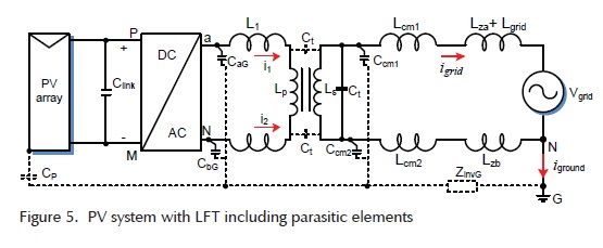
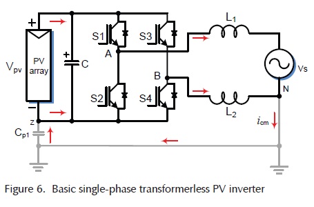
As can be observed in Figure 5, a possible path for the CMC between the electrical grid and the generator is through Ct. Ct is a parasitic capacitance located between the primary and the secondary winds in the LFT. The typical value of these capacitances is in the order of hundreds of picofarads, thus, the impedance of this capacitances is high at the low and medium switching frequency range (< 50 kHz), therefore, the CMC through the ground path is strongly reduced. Then, if the system is designed with a LFT, the common mode behaviour has no significant influence in the selection of the power converter topology and its modulation technique. On the other hand, if the LFT is omitted in the circuit as is depicted in Figure 4, then a path for the CMC exists. A common mode model, of the transformerless converter can be derived from the circuit shown in Figure 6 (Gubía et al., 2007). The common mode model is shown in Figure 7, as it can be observed, there are two main pulse voltage sources named VCMV which corresponds to the CMV and Vs1, which represent the influence of the differential mode voltage (VDMV) in the common mode behaviour. The total CMV represented by VCMV-tot can be obtained by adding the above mentioned voltage sources. According to the model, it can be easily derive that if the VCMV-tot doesn’t have high dv/dt (ideally constant), then no CMC will flow through the circuit.
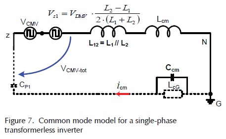
In accordance with the common mode model and specially with the equation for the pulse voltage source Vs1, there is a remarkable influence in the common mode behaviour related to the position of the filter inductance, thus if the inductance is separated in two equal parts located in the line and neutral wires, then Vs1 will be close to zero, otherwise, Vs1 will influence the common mode behaviour.
Commercial transformerless topologies
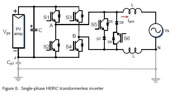
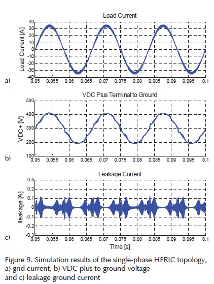
There are two outstanding single-phase transformerless inverter topologies in the market, called HERIC (Highly Efficiency and Reliable Inverter Concept) and H5. These topologies have been well received in the PV market due to their very good performance regarding efficiency and CMV. The HERIC topology which is presented in Figure 8 is based in the conventional HB (H-Bridge) inverter, but in this case an extra bidirectional switch (formed by S5, S6, D7 and D8 in Figure 8) is used on the ac side. The function of the bidirectional switch is to provide the zero states during the positive and negative semi-cycles of the grid period. Considering the modulation strategy reported in Schmidt et al., (2005), simulation results were performed using PSIM software and the results are shown in Figure 9. The output filter was set using an L filter split into two equal parts, one located in the line path and the other one located in the path that the current uses to return to the power source (in this case the PV panel), being 2.5 mH in each line. The filter was configured in this way because it has been shown that if differences in the output filter appear in both lines of the load, it will contribute to increase the value of the common mode currents (Xiaomeng et al., 2011; Guocheng et al., 2012; Barater-Buticchi et al., 2012). The dc bus was set using a constant dc source which was set at 600 V. Moreover, in order to evaluate the leakage current behavior a 150 nF stray capacitance was considered in the positive and negative terminals of the dc source. The switching frequency was set at 10 kHz while the grid source was set at 220 V and 60 Hz. The reference for the power injected to the grid was set to 4000 W. In Figure 9, from top to bottom, load current, voltage between the positive terminal and ground and leakage current are depicted. As can be seen, the load current is sinusoidal as expected and also the voltage measured between the positive terminal of the dc source and ground has a sinusoidal component at grid frequency, this means that the dv/dt applied to the parasitic capacitor is very slow and as a consequence the leakage ground current is close to zero.
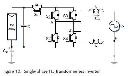
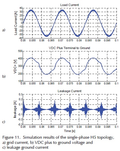
As it was mentioned, the H5 is another inverter topology with great success in the PV market (Victor et al., 2005). The topology is depicted in Figure 10. The topology is also based in the HB configuration but in this case, the zero state in the modulation strategy is generated by a switch S5 and a switch of the HB (S2 or S4). Hence the zero state is made on the dc side (dc-decoupling), while the active states are made using the HB circuit as in the HERIC topology. Simulation results of this topology under the same conditions than the HERIC converter are shown in Figure 11 where the grid current appears at the top, the voltage measured between the positive terminal and ground appears in the middle and finally the leakage current at the bottom. As it can be observed, the current in this case is sinusoidal, the voltage measured between the positive terminal and the ground has also a sinusoidal component at the grid frequency which has a very low dv/dt , and finally it can be noted that the leakage current is close to zero.
The topologies shown in this section have demonstrated the capability of achieving an excellent performance regarding efficiency (around 98% in both cases) as reported in Victor et al., (2005) and Schmidt et al., (2005). In the HERIC converter case, the additional components are switched at the grid frequency resulting in low switching losses. On the other hand, in the case of the H5 converter the additional component (S5) is switched at the switching frequency while S1 is switched at grid frequency, also resulting in low switching losses. Therefore, if only few additional power devices are added to the circuit and an optimized modulation strategy is implemented, the energy conversion process can be made with a good performance regarding efficiency. Besides efficiency, HERIC and H5 comply with the standards that limit the maximum leakage current levels allowed.
Proposed topology
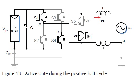
Given the characteristics described above about the HERIC converter (efficiency and CMV), a variant of this topology with its modulation strategy is proposed in this paper. The proposed topology and the circuit to generate the modulation sequence are depicted in Figure 12. The main idea is to generate the zero state using a modified bidirectional switch on the ac side. The modulation strategy proposed to control the inverter is as follow: during the positive half-cycle, the active state is generated when S1 and S4 are ON (S3 and S2 are OFF) while S5 is OFF and S6 is ON, therefore the current flows through S1 and S4 toward the load. In this situation, as shown in Figure 13, there is not current flowing through the bidirectional switch, due to the inverse polarization of D5. In order to generate the null state, S1 and S4 must be switched OFF while S6 remains ON. In this way, the current fl in the bidirectional switch through S6 and diode D5, because D5 is directly polarized due to the voltage generated by the energy stored in the inductance L; this is the freewheeling situation in the positive half-cycle as shown in Figure 14.
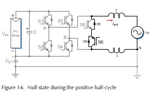
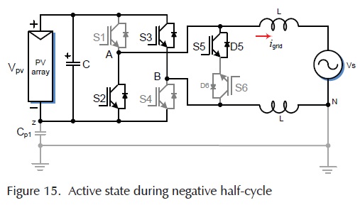
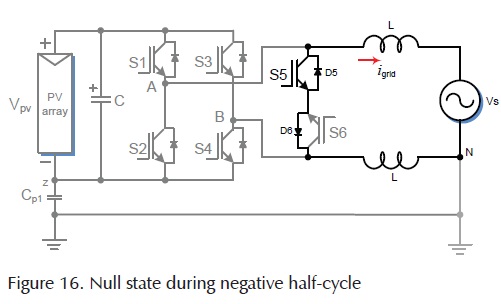
On the other hand, during the negative half-cycle, the active state is generated using S2 and S3 (S1 and S4 are OFF) as in the conventional HB inverter, while S5 is ON and S6 is OFF. During this state the current flows toward the load through the switches S2 and S3 as shown in Figure 15. The load current does not flow through the bidirectional switch because of the inverse polarization of D6. The null state during the negative half-cycle is generated when S3 and S2 are switched OFF while S5 remains ON. Therefore the load current will flow through the bidirectional switch (S5 and D6), because D6 is directly polarized due to the voltage generated by the energy stored in the inductance L, as it is shown in Figure 16.
The analysis of the equivalent circuits for the different operation modes along the grid period allows to obtain the CMV which is defined in (1) as the sum of the voltages from the output terminals to a common point (Barater et al., 2012).
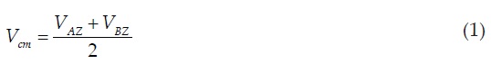
Using equation (1), the CMV generated regarding positive, negative and zero vectors, can be calculated as follow:
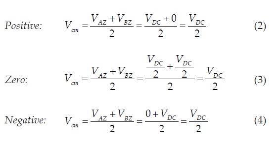
As can be observed from (2) to (4), the CMV remains constant along the different switching states. Under these conditions, it should be expected that just a very small leakage current will appear across the stray capacitances. In the next section, the numerical results show the performance of the proposed topology.
Current control loop for grid tied converter
The main strategy used to control the grid tied PV power converters is the current mode control. This technique consists in calculating an adequate current reference to inject active power into the grid. Then, a current control loop is designed based in the model of the system. Additionally, a Phase-Locked Loop (PLL) can be used to synchronise the injected current whit the grid voltage. The numerical results presented in this paper have been developed considering this control strategy. In this section the outlines to develop a current mode control are presented.
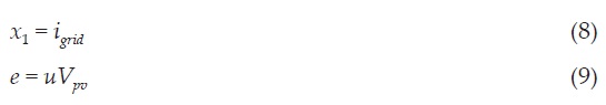
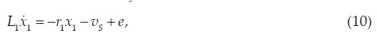
For the single-phase transformerless converter shown in Figure 12 the current dynamic can be modeled as
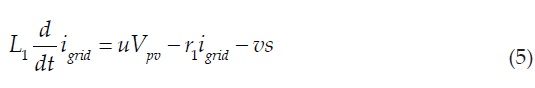
The parameter L1 represents the total value of the inductance output filter and r1 the parasitic resistance associated to the output filter. The control variable u is a continuous signal obtained from the switching function and considered in this way, given that the average model of the system is obtained. Notice that Vpv represents a continuous and regulated voltage. The voltage regulation can be reached by a voltage regulation loop that additionally includes a Maximum Power Point Tracking (MPPT) scheme.
i) Control objectives
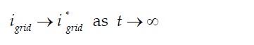
The control objective for the current dynamic are described next. The current tracking objective is designed to guarantee the tracking of the line current towards a current reference signal i*grid, that is
The current reference signal can be constructed in different ways, but for the grid tied applications it is proposed as a signal proportional to the fundamental of the grid voltage. Therefore, an adequate definition of the current reference avoids the injection of reactive and harmonic power in to the grid. Then the current reference is calculated as
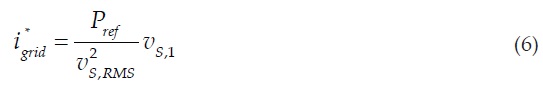
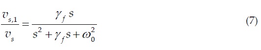
Where vS,1 is the fundamental component of the line voltage and Pref is a modulating current signal calculated in an outer voltage loop.
The fundamental component vS,1 is obtained by an additional PLL as is mentioned in Escobar et al. (2013) with the following structure
ii) Current control loop design
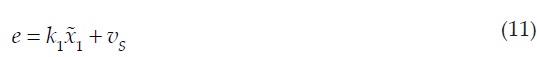
In order to simplify the control design, the following transformations are proposed
Then the current dynamic can be rewritten as
where the following controller stabilizes the subsystem (10) and is able to track with a very small steady state error the current reference signal i*grid
Notice that, the proposed control scheme is not able to guarantee a perfect tracking, this can be observed in slight current deformations or in small current lags with respect to the grid voltage phase. A solution for this issue is to place a Proportional plus Resonant controller in the current loop; but this issue is out of the scope of this paper.
Numerical results
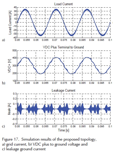
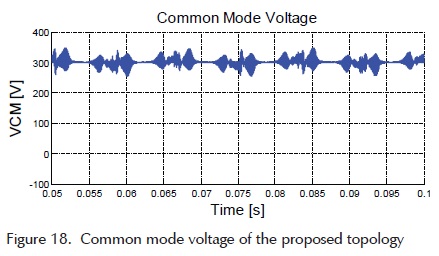
The proposed topology and its modulation strategy were tested by simulation with the same parameters used in the case of H5 and HERIC topologies. The results are shown in Figure 17, from top to bottom, the load current, the voltage measured between the positive terminal and ground (also called "Leakage Voltage") and the leakage current are depicted. As shown, the load current is close to a sinusoidal waveform with a current ripple at the switching frequency that depends on the output filter design, which is not a matter of study in this paper. Moreover, the voltage across the stray capacitance has a sinusoidal component resulting in a low dv/dt, see Figure 17b. A low dv/dt means that the leakage current will be low as the numerical results shown in Figure 17 c. Thus, the maximum peak that the leakage current reaches is around 100 mA that comply with the standard DIN VDE 0126-1-1. Finally, in Figure 18 the CMV is calculated for the proposed topology based in (1). As can be observed, the CMV is almost constant, which verifies the calculus performed above.
In a PV system, the power conversion efficiency is one of the most important parameters that must be considered in the design of the power converter. Therefore, it is a matter of study to analyze the power losses caused by the switching and conduction of the power devices. Hence an evaluation of the efficiency for the three topologies exposed in this paper is carried out.
The power losses were evaluated by using PSIM-Thermal Module. Equation (12) is used to calculate the conduction losses in a diode when it is conducting continuously. When the diode is conducting periodically with an on duty cycle of D, the conduction losses are calculated using equation (13).
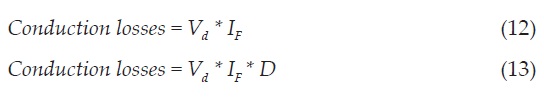
where Vd is the diode voltage drop and IF is the diode forward current.
The turn-on losses in the case of a diode are neglected. The turn-off losses due to the reverse recovery effect in the diode are calculated using equation (14) or equation (15),
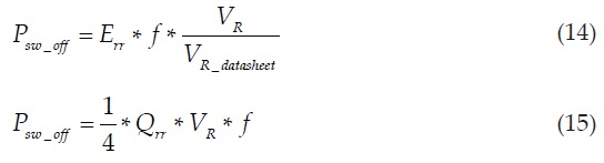
where Err is the reverse recovery energy losses, Qrr is the reverse recovery charge, f is the switching frequency VR is the actual reverse blocking voltage, and VR_datasheet is the reverse blocking voltage in the Err characteristic of the datasheet, defined as "Reverse blocking voltage VR (V)" in the test conditions.
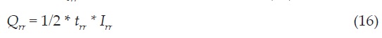
The Qrr can be defined by equation (16) a:
Whenever Err is given in the datasheet, the losses will be calculated based on Err, if Erris not given, the losses will be calculated based on Qrr , if Qrr is not given, the losses will be calculated based on trr and Irr, if both are no given the losses will be treated as 0.
In the case of an IGBT the conduction losses are calculated by using equation (17) when the transistor is conducting continuously. When the transistor is conducting periodically, then the losses are calculated based on the duty cycle D using equation (18).
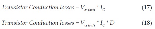
where Vce(sat) is the collector-emisor saturation voltage and IC is the collector current.
The switching losses during the turn-on and turn-off transitions are calculated with equations (19) and (20) respectively.
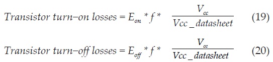
where Eon and Eoff are the turn-on and turn-off energy losses respectively, f is the switching frequency, Vcc is the actual dc bus voltage, and Vcc_datasheet is the dc bus voltage in the Eon and Eoff characteristics of the datasheet, defined as "dc bus voltage (V)" in the test conditions. The power losses in the case of the antiparallel diode in the IGBT are calculated as in the case of the discrete diode explained above.
The IGBT used to evaluate the switching and conduction losses was the IPM75DSA120 with 1200 V and 75A of rated voltage and current respectively. The IGBT model was loaded in the database of PSIM using the manufacturer's datasheet. The calculated efficiency provided by PSIM only considers the power losses in the semiconductors which are the devices where the major power losses occur. Moreover, in order to consider the power losses behavior under different operating conditions, the power reference was set for different injected power levels giving the results summarized in the plots shown in Figure 19.
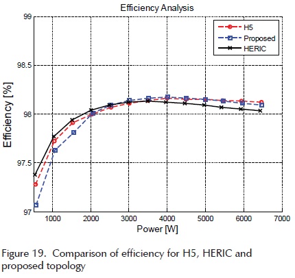
As it can be observed, the proposed inverter has a similar performance than the commercial topologies regarding efficiency. However, it can be seen that in the case of the proposed topology the efficiency is a bit higher than the efficiency of the HERIC topology. This is because the proposed topology does not use additional diodes in the implementation of the bidirectional switch.
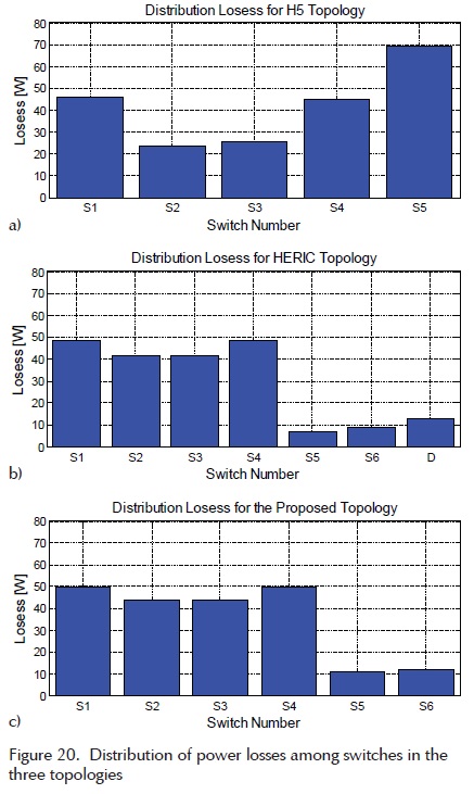
Furthermore, the power losses in each IGBT can be calculated to determine how the power losses are distributed among all power switches. In Figure 20, the distribution losses for the three transformerless topologies exposed in this paper are depicted. As it can be observed in the case of Figure 20a, which corresponds to the H5 topology, the major losses are concentrated in the switch S5, then, special care must be considered in the thermal design for this switch. In the case of Figure 20b, which is the case of HERIC topology, the power losses are quiet balanced for all the switches. In terms of thermal design, this topology has a better performance than the H5 topology, because in this case, all the switches are operating more or less at same temperature. It can be noticed that there is an extra bar (D) which corresponds to the power losses in the diodes used in the bidirectional switch. Finally, in the case of the proposed topology, which is depicted in Figure 20c, the distribution power losses is close to the case of HERIC topology, but in this case, the losses in the diodes D5 and D6 do not appear. Therefore in the case of the proposed topology the thermal design can be performed in a simpler way and at a lower cost.
Conclusions
Transformerless photovoltaic converters offer higher efficiency than those that use a transformer as an isolation stage. A problem regarding generated common mode voltage arises when the galvanic isolation is omitted in the power conversion system. In general, the common mode voltage behavior is determined by the topology structure and its PWM strategy. The variations in the common mode voltage impact significantly the leakage current through the stray capacitance of the PV module. In order to reduce or eliminate the leakage currents, a topology has been proposed in this paper.
The proposed topology is based in the HERIC inverter, where an alternative bidirectional switch is implemented using only two IGBTs instead of two IGBTs and the two diodes that uses the HERIC topology. The proposed topology was simulated using the proposed bidirectional switch and it was compared with two popular transformerless topologies regarding ground currents and efficiency. The modulation strategy implemented in the simulations of the topologies is based on the classical unipolar sinusoidal pulse width modulation, which provides a voltage such that the filtering requirements are less demanding. In the case of the ground current behavior, the three topologies have a similar performance being a low leakage current the common characteristic that complies with the requirements defined in the standard DIN VDE 0126-1-1. However, in the case of the efficiency, the simulation results show that for power levels between 1 kW and 2 kW, the proposed topology has a lower efficiency than H5 and HERIC topologies. Nonetheless, for power levels between 2 kW and 6 kW, the efficiency is similar between the proposed topology and the H5 topology, while HERIC topology presents the lowest efficiency for this interval. Notice that most of the commercial PV inverters for low power applications are on the set of 2 kW to 10 kW.
In this paper a transformerless topology was introduced which focuses in providing an alternative solution for the bidirectional switch implemented as an ac-decoupling. The numerical results show that the CMV of the proposed topology remains almost constant along the grid period. On the other hand, the efficiency of the proposed topology can be competitive with the popular ones. Therefore, it can be concluded that the proposed topology can be a very attractive solution for the PV transformerless applications.
References
Barater-Buticchi D., Crinto G., Franceschini A., Lorenzani G. Unipolar PWM strategy for transformerless PV grid-connected converters. IEEE Transactions on Energy Conversion,volume 27 (issue 4), 2012: 835-843. [ Links ]
DKE Deutsche Kommission Elektrotechnik Elektronik Informationstechnik im DIN und VDE, DIN VDE 0126-1-1, 2005. [ Links ]
Gonzalez R., Gubia E., Lopez J., Marroyo L. Transformerless single-phase multilevel-based photovoltaic inverter. IEEE Transactions on Industrial Electronics, volume 55 (issue 7), 2008: 2694-2702. [ Links ]
Gonzalez R., Lopez J., Sanchis P., Marroyo L. transformerless inverter for single-phase photovoltaic systems. IEEE Transactions on Power Electronics.volume 22 (issue 2), 2007: 693-697. [ Links ]
Gubía E., Sanchis P., Ursúa A., López J., Marroyo L. Ground currents in single-phase transformerless photovoltaic systems. Progress in Photovoltaic: Research and Applications, volume 15 (issue 7), 2007: 629-650. [ Links ]
Guocheng S., Qi H., Junjuan W., Xiaoqiang G. A new three-level six-switch topology for transformerless photovoltaic systems, in: 2012 7th International Power Electronics and Motion Control Conference (IPEMC), 2012, pp.163-166. [ Links ]
Hou C., Shih, C., Cheng P., Hava A.M. Common-mode voltage reduction pulsewidth modulation techniques for three-phase grid-connected converters, IEEE Transactions on Power Electronics, volume 28 (issue 4), 2013:1971-1979. [ Links ]
Ji B., Wang J., Zhao J. High-efficiency single-phase transformerless pv h6 inverter with hybrid modulation method. IEEE Transactions on Industrial Electronics, volume 60 (issue 5), 2013: 2104-2115. [ Links ]
Kerekes T., Liserre M., Teodorescu R., Klumper C., Summer M. Evaluation of three-phase transformerless photovoltaic inverter topologies. Transactions on Power Electronics, volume 24 (issue 9), 2009: 2202-2211. [ Links ]
Kerekes T., Teodorescu R., Borup U. Transformerless photovoltaic inverters connected to the grid, in: Twenty Second Annual IEEE in Applied Power Electronics Conference, APEC 2007, 2007, pp.1733-1737. [ Links ]
Kjaer S., Pedersen J., Blaabjerg F. A review of single-phase gridconnected inverters for photovoltaic modules. Transactions on Industry Applications, volume 41 (issue 5), 2005: 1292-1306. [ Links ]
Li Q., & Wolfs P. A Review of the single phase photovoltaic module integrated converter topologies with three different dc link configurations. IEEE Transactions on Power Electronics, volume 23 (issue 3), 2008: 1320-1333. [ Links ]
Lopez O., Teodorescu R., Freijedo F., Doval-Gandoy J. Eliminating ground current in a transformerless photovoltaic application. IEEE Transactions on Energy Conversion, volume 25 (issue 1), 2010: 140-147. [ Links ]
Salm T., Bouzguenda M., Gastli A., Masmoudi A. A novel transformerless inverter topology without zero-crossing distortion. International Journal Of Renewable Energy Research, volume 2 (issue 1), 2012: 140-146. [ Links ]
Schmidt H., Siedle C., Ketterer J. (n.d.). Patent No. EP 1 369 985 A2, 2005. [ Links ]
Vazquez G., Kerekes T., Rocabert J., Rodríguez P., Teodorescu R., Aguilar D. A photovoltaic three-phase topology to reduce Common Mode Voltage, in: IEEE International Symposium on Industrial Electronics, 2010, pp. 2885-2890. [ Links ]
Victor M., Greizer F., Bremicker S., Hubler U. Patent No. EP 1 369 985 A2, Germany, 2005. [ Links ]
Xiaomeng S., Yaojie S., Yandan L. Analysis on leakage current in transformerless single-phase PV inverters connected to the grid, in: 2011 Asia-Pacific power and energy engineering conference (APPEEC), 2011, pp. 1-5. [ Links ]
Xue Y., Chang L., Baekhøj-Kjaer S., Bordonau J., Shimizu T. Topologies of single-phase inverters for small distributed power generators: an overview. IEEE Transactions on Power Electronics, volume 19 (issue 5), 2004: 1305-1314. [ Links ]
Yang B., Li W., Gu Y., Cui W., He X. Improved transformerless inverter with common-mode leakage current elimination for a photovoltaic grid-connected power system. IEEE Transactions on Power Electronics, volume 27 (issue 2), 2012: 752-762. [ Links ]
Escobar G., Valdez A.A., Martínez P.R., Sosa J.M., Limones Pozos C.A. A model-based controller for the cascade H-bridge Multilevel converter used as a shunt active filter. IEEE Trans. Ind. Electronics, volume 60 (issue 11), 2013: 5019-5028. [ Links ]
Citation for this article:
Chicago citation style
Vázquez-Guzmán, Gerardo, Pánfilo Raymundo Martínez-Rodríguez, José Miguel Sosa-Zúñiga. High Efficiency Single-Phase Transformerless Inverter for Photovoltaic Applications. Ingeniería Investigación y Tecnología, XVI, 02 (2015): 173-184
ISO 690 citation style
Vázquez-Guzmán G., Martínez-Rodríguez P.R., Sosa-Zúñiga J.M. High Efficiency Single-Phase Transformer-less Inverter for Photovoltaic Applications. Ingeniería Investigación y Tecnología, volume XVI (issue 2), April-June 2015: 173-184.
About the authors
Gerardo Vázquez-Guzmán. Was born in México in 1977. He received the B.Sc. degree in electronic engineering from the Technical Institute of Apizaco, Tlaxcala, México, in 2003, the M.S. degree in electronic engineering from the National Center of Research and Technological Development, Cuernavaca, México, in 2006 and the PhD. degree in Electrical Engineering from the Technical University of Catalonia (UPC) in Barcelona, Spain, in 2013. Since September 2012 he is with the department of electronics in the Technological Institute of Superior Studies of Irapuato (ITESI) where he holds a Professor/Researcher position. His research interests include power converters and control for nonconventional energy sources.
Pánfilo Raymundo Martínez-Rodríguez. Received the Ph.D. degree from the Potosi Institute of Scientific and Technological Research (IPICyT), Mexico, in 2007. In August 2006, he joined the Technological Institute of Superior Studies of Irapuato (ITESI), Mexico, where he is currently a Professor/Researcher. His main research interests include modeling, analysis and control design for power electronic systems and renewable energy systems.
José Miguel Sosa-Zúñiga. Received the Ph.D. degree in Applied Sciences from the Potosi Institute of Scientific and Technological Research (IPICYT), Mexico, in 2009. He is currently with the Technological Institute of Superior Studies of Irapuato (ITESI) where he holds a Professor/Researcher position since 2008. His current research interests include nonlinear control theory and applications to underactuated mechanical systems, and power electronics converters control design for renewable energy applications.

