


Services on Demand
Journal
Article
 English (pdf)
 Article in xml format
 Article references
 Send this article by e-mail
Indicators
-
 Cited by SciELO
 -
 Access statistics
Related links
-
 Similars in
SciELO
Similars in
SciELO
Share

 Permalink
Ingeniería, investigación y tecnología
On-line version ISSN 2594-0732Print version ISSN 1405-7743
Ing. invest. y tecnol. vol.11 n.3 Ciudad de México Jul./Sep. 2010
Electrical Parameters Extraction of CMOS Floating–Gate Inverters
Extracción de parámetros eléctricos de inversores CMOS de compuerta flotante
Molinar–Solís J.E.1, Ponce–Ponce V.H.2, R.Z. García–Lozano3, Díaz–Sánchez A.4 y Rocha–Pérez J.M.5
1 Universidad Autónoma del Estado de México, E–mail: Jemolinars@uaemex.mx
2 Centro de Investigación en Computación, Instituto Politécnico Nacional, México, E–mail: vponce@cic.ipn.mx
3 Universidad Autónoma del Estado de México, E–mail: zolagarcia@yahoo.com
4 Instituto Nacional de Astrofísica, Óptica y Electrónica INAOE, Tonantzintla, Puebla, E–mail: adiazsan@inaoep.mx
5 Instituto Nacional de Astrofísica, Óptica y Electrónica INAOE, Tonantzintla, Puebla, E–mail: jmr@inaoep.mx
Recibido: septiembre de 2008
Aceptado: julio de 2009
Abstract
This work provides an accurate methodology for extracting the floating–gate gain factory, of CMOS floating–gate inverters with a clock–driven switch for accessing temporarilly to the floating–gate. With the methodology proposed in this paper, the γ factor and other parasitic capacitances coupled to the floating–gate can be easily extracted in a mismatch–free approach. This parameter plays an important role in modern analog and mixed–signal CMOS circuits, since it limits the circuit performance. Theoretical and measured values using two test cells, fabricated in a standard double poly double metal CMOS AMI–ABN process with 1.2 µm design rules, were compared. The extracted parameters can be incorporated into floating–gate PS pice macromodels for obtaining accurate electrical simulation.
Keywords: FG–inverter, neuMOS, floating–gate.
Resumen
En este trabajo se brinda una metodología precisa para la extracción del factor de ganancia γ de la compuerta flotante en inversores CMOS, que constan de un interruptor para acceder temporalmente a la compuerta flotante. Con la metodología propuesta, el factor γ y otras capacitancias parásitas acopladas a la compuerta flotante pueden ser extraídas. Estos parámetros son de mucha importancia, ya que juegan un papel importante en el desempeño de circuitos analógicos y de señal mixta. La comparación entre cálculos teóricos y simulaciones es hecha utilizando dos celdas de prueba fabricadas de tecnología AMI ABN de 1.2 µm, a través de la organización MOSIS. Los parámetros extraídos pueden ser incorporados a macromodelos en PSpice para obtener simulaciones más precisas.
Descriptores: inversor de compuerta flotante, NeuMOS, compuerta flotante.
Introduction
The CMOS floating–gate inverters with multiple inputs have become a useful circuit block in modern analog and mixed–signal circuit design. A CMOS floating–gate inverter is a typical CMOS inverter with two or more input capacitances coupled to the floating gate (FG), which is common to both N and P channel enhancement MOSFET transistors which are connected in the drain mode. The potential induced in the FG can be controlled as a weighted linear sum, in voltage–mode, of all input signals. The potential of the FG establishes the on–off state of the CMOS inverter (Shibata et al, 1992–1993).
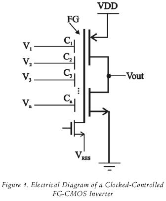
Discharging of the FG is commonly required but also, for many applications, it is desirable to pre–charge the FG to a given bias voltage. Discharging and pre–charging the FG can be achieved by using an analog switch that connects temporally the FG to an externally applied potential (VRES). By using an external voltage VRES = 0V, the FG can be discharged and the typical UV erasing technique can be avoided (figure 1). This concept has been introduced first in (Kotani et al, 1995–1998) and was named as clocked–controlled NeuMOS inverter, but it will be referred as clocked–controlled FG–CMOS inverter.
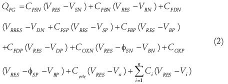
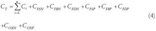
The FG gain factor γ, determines the maximum input contribution to the FG potential. For n capacitive inputs it is expressed as:
Where CT is the total capacitance including parasitic capacitances. The physical characterization of the FG gain factor γ, also known as the capacitive coupling coefficient, and the parasitic capacitances coupled to the FG, is a fundamental step in the design of high performance FG–CMOS based circuits, since the device behavior strongly depends on these values. The strategy followed in this work consists in comparing some features of the transient behavior in the "reset" and "evaluation" periods. One advantage of this approach is that the extraction of the above mentioned parameters can be done to the FG inverter without the use of a "dummy cell" (Mondragón et al, 2000), resulting in an accurate mismatch–free techniques, and whose evaluation will be demonstrated by comparing theoretical and measured results in the next sections.
Clock–controlled FG–CMOS inverter
Electrical charge and potential in the FG using an ideal analog switch
The electrical equivalent circuit for the FG inverter showing the control and relevant parasitic capacitances is shown in figure 2.
According to figure 1, the total charge stored in the FG, QFG is given by:
where Ci, is the capacitance between the FG and the input node i, Vi is the ith input voltage, VDN, VDP, VSN , VSP and VBN , VBP are the drain, source and substrate voltages for the NMOS and PMOS transistors, respectively. From now on, the right side subscripts N and P will denote NMOS and PMOS, respectively. CFDN,, CFDP and CFSN,, CFSP are the overlap capacitances between the FG and the drain or source, respectively. CFBN , and CFBP are the overlap capacitances between the FG and the bulk along the edge of the channel, COXN and COXP are the gate oxide capacitances, CDFPN and CDFPP in figure 2, are the depletion layer capacitances, which can be neglected after the channel begins to form the floating gate (Shibata et al., 1993). Potentials φSN and φSP represent the surface potential of the silicon substrate. Cpoly is the parasitic capacitance between the FG (polysilicon back–plate) and the below substrate layer tied to a Vx potential. In this case, for a P– substrate Vx = GND. Potential VRFS is the voltage transferred to the FG through the switch. All voltages in (2) are relative to substrate.
It is assumed that no charge injection and no charge leakage occur during device operation. Then, from the charge conservation law on the FG, (2) can be simplified and rearranged to obtain an expression for the potential on the FG, VFG, when the initial net charge is zero, this is given by:
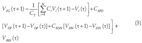
where the potentials at the reset period are represented by ( ), this is, when the reset switch is closed, and the potentials at the evaluation period represented by (+1), when the switch is open. In (3), Vi(+ 1) represents the ith input voltage during the evaluation period, and Vi() is the ith input voltage applied during the reset period. The remaining potentials terms, coupled to the FG do not contribute with charge in both periods, but their associated capacitances contribute to form CT, which is defined as the sum of all capacitances coupled to the FG as follows.
Potential in the FG using a real analog switch
For practical implementations, a single N–channel MOSFET can be used in stead of the SW element as shown in figure 2. In figure 3, an equivalent circuit for the FG inverter using a real switch is introduced.
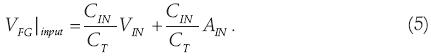
If the access switch transistor (SW) is ni cut off region, a simplest electrical equivalent circuit for the FG potential can be obtained (Ramírez et al., 2004), figure 4, where all the inputs are tied together and form a single input capacitor CIN, CIN = C1+...+Ci+...+Cn. Capacitance COUT represents the sum of CFDP and CFDN. The Cpi capacitor is the ith parasitic capacitance that couples the FG to a DC voltage VDCi.
Here, the ideal diode element models the N+/P parasitic drain–bulk junction, associated to the access switch transistor (SW) in cut off and Rleak is an approximation to the non–linear leakage resistance of this junction.
The input VIN voltage contribution to the FG potential can be obtained through the solution of a simplified circuit (figure 5a).
Where the capacitance CT' is defined as CT' =CT – CIN. By conducting a Thevenin reduction to the circuit, the clamping circuit in figure 5b is obtained. For any period ical and continuous voltage signal applied to the circuit, VIN =AIN f1(t+nT) with amplitude AIN and period T, such that T << RleakCT, figure 5c, the FG potential due only to this input–signal, figure 5d, will be given by:
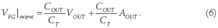
The same analysis holds for the corresponding contribution on the FG potential as a function of a periodical output signal VOUT=AOUT f2(t+nT), coupled to the FG through COUT, as follows:
For the DC contribution, the following analytical time–domain expression for the FG potential is obtained:
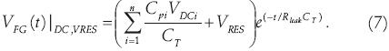
The global expression that models the FG potential will be obtained by summing equations (5), (6) and (7), this is:

During the evaluation period, the terms associated to DC potentials coupled to the FG, vanish for t>>RleakCT. This means that the induced DC–charge on the FG at circuit startup and the reset–charge due to VRES, will be swept out during the evaluation period, after several circuit–time constants RleakCT. Therefore, in steady–state, the FG potential will be:
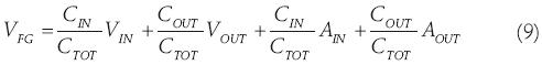
By deriving equation (9) with respect to time, the following expression is obtained
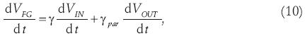
where, γ=CIN/CT is the FG gain factor and γpar= COUT/CT would correspond to a parasitic FG gain factor due to the feedback of the FGMOS inverter's output voltage on the FG.
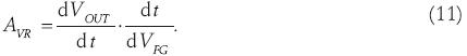
In reset mode, applying a direct signal to the FG, i.e. a sawtooth, the slope of the inverter transfer characteristic associated to the circuit shown in figure 6a, is given by:
In a similar way, as illustrated in figure 7a, the slope of the transfer characteristic, when the circuit operates in the evaluation period, is given by
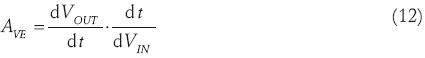
Now substituting (11) and (12) in (10), the following relation is obtained:
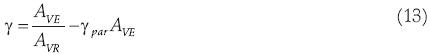
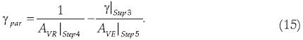
Where, the slopes AVE and AVR can be easily measured in order to extract the parameters γ and γpar
Extraction methodology
The basic idea that supports the extraction methodology consists in comparing the inverter transient response obtained in the reset period with that obtained during the evaluation period. The extraction methodology is presented next as a sequence of six steps:
Step 1. A measurement during the reset period of AVR is taken around a fixed point in VIN which corresponds to a low–gain slope of the output characteristic (VOUT), (figure 6b).
Step 2. A measurement during the evaluation period of AVE is taken around the same point of step 1, (figure 7b).
Step 3. Parameter γ is calculated using (13). The second term of the right side of this equation is negligible in the low–gain region due to γpar<γ and since AVE is small, then, γ approaches to
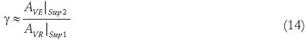
Step 4. A measurement during the reset period of AVR is taken at a fixed point VIN near the switching–point of the inverter, which corresponds to a high–gain slope of the output characteristic, (figure 6b).
Step 5. A measurement in the evaluation period of AVE is taken at the same point of step 4, see figure 7b.
Step 6. From (13), γ is calculated using the values obtained in the steps 3, 4 and 5, by using
Experimental results
Two test cells were fabricated using a double–poly double–metal CMOS process with 1.2µm design rules, available through MOSIS services (run: T2AH–BJ and T48S–AM). The microphotograph of each test cell is shown in figure 8. The first test cell corresponds to the circuit introduced in figure 6a. The schematic diagram for the second test cell is not shown, but is a six–input FG–CMOS inverter.
The test cells were measured using the described methodology presented in section 3. The small–signal slopes were computed by using a linear–fit approximation from data points obtained by means of a digital oscilloscope. Table 1, shows the theoretical and extracted values for γ and γpar using a 100 kHz saw–tooth signal with 5V peak–to–peak and a 2.5V offset. The period of this signal (T=10µs) is smaller than the intrinsic circuit–time constant which normally is in the order of seconds.
Discussion
Although the theoretical capacitance values can be calculated using the process parameters given by the foundry, the physical differences of the input capacitances can lead to an important deviation of γ factor and thus affecting significantly the circuit operating point. As an example, two identical CMOS inverters were simulated through PSpice, one of them with an input capacitance deviation of 5% (figure 9a).
The inverters outputs are shown in figure 9b. The switching operating point (Jacob et al., 1998) of the inverters as shown, is shifted near by 60mV with respect the input voltage Vin , this condition is undesirable for many analog and mixed signal applications since the recent low–voltage trends requires high accuracy. The methodology presented in this work focuses on CMOS floating–gate circuits with a clock–driven switch at the FG, and represents a good choice when the γ factor must be determined experimentally for high accuracy requirements.
Acknowledgements
Mexico State Autonomous University (CU UAEM–Ecatepec), Interdisciplinary Professional School of Engineering and Advanced Technologies (UPIITA–IPN) and National Institute for Astrophysics, Optics and Electronics, INAOE.
References
Shibata T., Ohmi T. A Functional MOS Transistor Featuring Gate–Level Weighted Sum and Threshold Operations. IEEE Trans. on Electron Devices, 39(6): 1444–1455, 1992. [ Links ]
Shibata T., Ohmi T. Neuron MOS Binary–Logic Integrated Circuits – Part I: Design Fundamentals and Soft–Hardware–Logic Circuit Implementation. IEEE Trans. on Electron Devices, 40(3):570–576, 1993. [ Links ]
Kotani K., Shibata T., Imai M., Ohmi T. Clocked– Neuron–MOS Logic Circuits Employing Auto–Threshold–Adjustment. On: IEEE International Solid–State Circuits Conference ISSCC95, 1995, pp. 320–322. [ Links ]
Kotani K., Shibata T., Imai M., Ohmi T. Clock–Controlled Neuron–MOS Logic Gates. IEEE Trans. on Circuits and Systems– II: Analog and Digital Signal Processing, 45(4): 518–522, 1998. [ Links ]
Mondragon–Torres A., Shneider M., Sanchez–Sinencio E. Extraction of Electrical Parameters of Floating Gate Devices for Circuit Analysis, Simulation, and Design. On: The 2002 45th Midwest Symposium on Circuits and Systems, 2002. MWSCAS–2002, Vol. 1, 2000, pp. 311–314. [ Links ]
Shibata T., Ohmi T. Neuron MOS Binary–Logic Integrated Circuits – Part II: Simplifying Techniques of Circuit Configuration and their Practical Applications. IEEE Trans. on Electron Devices, 40(5):431–434, 1993. [ Links ]
Ramirez–Angulo J., Lopez–Martin A., Gonzalez–Carbajal R., Muñoz–Chavero F. Very Low–Voltage Analog Signal Processing Based on Quasi–Floating Gate Transistors. IEEE Journal of Solid State Circuits, 39(3):434– 442, 2004. [ Links ]
Ramirez–Angulo J., González–Altamirano G., Choi S.C. Modeling Multiple–Input Floating–Gate Transistors for Analog Signal Processing. On: International Symposium On Circuits and Systems ISCAS'97, Vol. 3, 1997, pp. 2020–2023. [ Links ]
Guan H., Tang Y.S. Accurate and Efficient Models for the Simulation of Neuron MOS Integrated Circuits. International Journal of Electronics, 87, 2000, pp. 557–568. [ Links ]
Jacob–Baker R., Li H.W., Boyce D.E. CMOS Circuit Design, Layout and Simulation. IEEE Press series on Microelectronic Systems. USA. 1998. [ Links ]
About the authors
Jesús Ezequiel Molinar–Solis. Was born in Chihuahua, Mexico, in 1976. He received the electronics engineering degree from the Technological Institute from Ciudad Guzman (ITCG), Jalisco, in 1999. He obtained the M.Sc. and Ph.D. degrees in electrical engineering at the Center for Research and Advanced Studies (CINVESTAV–IPN), Mexico City, in 2002 and 2006 respectively. He is currently working as a Titular Professor with the Mexico State Autonomous University (UAEM) at Ecatepec, Estado de Mexico, his research interests are related to analog circuits, neural networks and vision chips.
Victor Hugo Ponce–Ponce. Received the B. Tech. degree in electronics engineering from the Superior School of Mechanical and Electrical Engineering (ESIME) of the National Polytechnic Institute (IPN) of Mexico, in 1993, and the M. of Sc. and Ph.D. degrees in electrical engineering from Center for Research and Advanced Studies (CINVESTAV–IPN) at Mexico City, in1994 and 2005, respectively. He is currently working as Professor at the Computer Research Centre CIC–IPN. His research interests include CMOS design circuits and vision sensors.
Rodolfo Zola Garcia–Lozano. Was born in Mexico City, Mexico in 1973. He received the electronics engineering degree from Technologic of Advanced Studies from Ecatepec (TESE), Mexico in 1996. He obtained the Ph.D degree in Electrical Engineering at the Center of Research and Advanced Studies (CINVESTAV–IPN), Mexico City, in 2005. He is currently working as a Titular Professor with the Mexico State Autonomous University (UAEM) at Ecatepec, Estado de Mexico. His research interests are related to electronics circuits and thin film devices application.
Alejandro Díaz–Sánchez. Received the B.E. from the Madero Technical Institute and the M.Sc. from the National Institute for Astrophysics, Optics and Electronics, both in México, and the Ph.D. in Electrical Engineering from New Mexico State University at Las Cruces, NM. He is actually working as Full Professor at the National Institute for Astrophysics, Optics and Electronics, in Tonantzintla, Mexico. His research concerns analog and digital integrated circuits, high performance computer architectures and signal processing.
José Miguel Rocha–Pérez. Was born in Huixcolotla, Puebla, México. He received the B.S. degree in electronics from the Universidad Autónoma de Puebla, Puebla, México in 1986 and the M.Sc. and Ph.D. degrees from the Instituto Nacional de Astrofísica Óptica y Electrónica (INAOE), Puebla, in 1991 and 1999, respectively. He was a Visiting Researcher in the Department of Electrical Engineering, Texas A&M University, College Station in 2002. Currently, he is working at INAOE in the Electronics Department and his current research interests are on the design of integrated circuits for communications.

