SciELO - Scientific Electronic Library Online

 
vol.20 número4A New Approach For Hand Gestures Recognition Based on Depth Map Captured by RGB-D CameraMedidas de diversidad para la construcción de sistemas multi-clasificadores usando algoritmos genéticos índice de autoresíndice de materiabúsqueda de artículos
Home Pagelista alfabética de revistas  

Servicios Personalizados

Revista

Articulo

Indicadores

Links relacionados

  • No hay artículos similaresSimilares en SciELO

Compartir


Computación y Sistemas

versión On-line ISSN 2007-9737versión impresa ISSN 1405-5546

Comp. y Sist. vol.20 no.4 Ciudad de México oct./dic. 2016

https://doi.org/10.13053/cys-20-4-2489 

Regular Articles

A 3μW Low-Power CMOS Class-AB Bilateral Current Mirror for Low-Voltage Applications

Jesús E. Molinar-Solís1 

Víctor H. Ponce-Ponce2 

José Rivera Mejía1 

Sergio Sandoval1 

Miguel Rocha Pérez3 

Alejandro Díaz-Sánchez3 

Humberto Bracamontes del Toro1 

1Tecnológico Nacional de México, Ciudad Guzmán Jalisco, Mexico. jemolinars@itcg.edu.mx, jrivera@itchihuahua.edu.mx, chekosur@gmail.com, hbdeltoro@gmail.com.

2Instituto Politécnico Nacional, Centro de Investigación en Computación, Mexico. vponce@cic.ipn.mx.

3Instituto Nacional de Astrofísica, Óptica y Electrónica (INAOE), Puebla, Mexico. jmr@inaoep.mx, adiazsan@inaoep.mx.


Abstract

This paper presents a compact low-power bidirectional current mirror suitable for low-voltage applications. The key element is the use of a CMOS complementary input stage working in subthreshold regime; which allows setting a reduced bias current through the mirror. The circuit was simulated using LTSpice and presents class AB operation with a THD of 1% at 1MHz. The power consumption is close to 3μW as shown by simulations and experimental data from a fabricated prototype using 0.5µm CMOS technology.

Keywords: Analog integrated circuits; MOS integrated circuits

1 Introduction

The current mirror is a basic analog building block which is widely used in OTA’s, OP-AMP´s and other complex current mode circuits. Nowadays low-power requirements lead analog designers to consider class AB circuits due to their low quiescent current features and their capability to handle currents several times larger. Besides, voltage supply shrinking in modern fine line technology reduces considerably the voltage headroom for analog design; hence, solutions capable to work with a low-voltage condition and class AB operation are mandatory.

Many class AB current mirrors have been proposed in the past. In 1, extra circuitry was included for achieving class AB operation but, this extra complexity increases the minimum voltage requirement for the overall circuit. Other class AB approaches 2-6 improves the input/output impedance of the current mirror, however do not work for bidirectional currents and they are not able to work for low-voltage applications.

The low impedance output node of the Flipped Voltage Follower (FVF) has been extensively used for many applications including current mirrors 5-6; in 6 the use of a FVF and a simple current mirror achieves class AB operation with lowvoltage conditions. Although it is an interesting proposal, it is desirable to get simpler solutions at least for some applications. In this work, a very compact bidirectional current mirror is presented, which is able to deal with currents much larger than the bias current.

This paper is organized as follows: In the next section the proposed circuit is presented and explained. Section 3 presents electrical simulations; section 4 experimental results and discussion and finally; in section 5 conclusions are given.

2 Compact Class AB Current Mirror

According to 7, a given circuit works in lowvoltage mode if its voltage supply VDD is less than the sum of the complementary threshold voltages of NMOS and PMOS, i.e. VDD<|VTHp| + VTHn.

In Fig. 1, a class AB current mirror proposed in 1 is shown. Here, transistors M3 and M4 set the bias current Ibias in the input branch. Therefore, these transistors can fix a reduced bias current for reduced static power consumption. Nevertheless, the branch of transistors M1 and M2 defines the minimum voltage supply requirement for the circuit, i.e. VDDmin=2VDSsat+VGSp+VGSn. Where VDSsat is the minimum MOS overdrive drain-source voltage for saturation condition and considered for current sources Ibias implemented by a single MOS transistor. VGSp is the MOS voltage gate-source which must fulfill VGSp>|VTHp| and VGSn> VTHn for operation in strong inversion regime.

Fig. 1 Class AB current mirror 

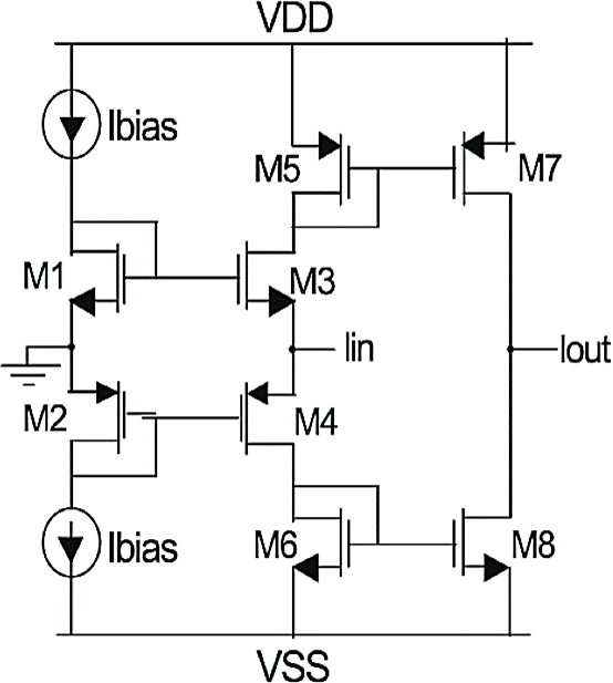
Using 0.5µm CMOS technology with threshold voltages VTHn=0.65V and |VTHp|=0.95V, the minimum supply for this circuit should be VDDmin=2VDSsat+VGSp+VGSn, i.e. VDDmin ≥ 2V. Thus, the proposal is not suitable for lowvoltage applications.

The proposed current mirror is presented in Fig 2. This circuit is a simplified version of the previous circuit. From Fig. 1, the absence of transistors M3 and M4 lead to the circuit in Figure 2. Since for low voltage operation VDDmin<|VTHp| + VTHn, must be fulfilled, this condition cause M1 and M2 in Fig 2, to work in moderate/weak inversion. The MOS subthreshold conduction at drain has an exponential dependency on VGS, for VDS>200mV 8, this is:

(1)

where VT = kT/q, and ζ >1 is a nonideality factor.

Fig. 2 Proposed current mirror 

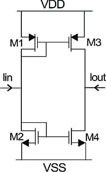
This special feature sets a very small bias current on both branches, preserving the class AB operation. Thus, when a given current Iin is introduced into the circuit the input node goes high turning M1 PMOS “off” and turning M2 NMOS “on”. Therefore, the input current is well copied by the M2-M4 mirror. In case Iin is extracted from the circuit, input node goes low, therefore, M2 NMOS is turned off and M1 turned on bringing Iin. In this case the input copy is achieved by the PMOS counterpart to the output.

The input resistance of the circuit is given simply by:
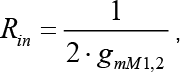
(2)

for the case gmM1 = gmM2 . The output resistance Ro is given in a similar way as Ro=1/(2gdsM3,4).

3 Simulation Results

The circuit proposed in Figure 2 was simulated using Spice with BSIM3 version 3.1 model parameters from ON Semi 0.5μm technology available through MOSIS. Transistors aspect ratios are W/L=30μm/1.5μm for all NMOS and PMOS transistors.

In Fig. 3, the bias current of the circuit is plotted against different VDD values. As can be noticed, bias current goes from several pA to μA. Nevertheless, in the range 1.4<VDD<1.6 the bias has a dependency on VDD of 500nA/100mV.

Fig. 3 DC simulations results, Bias current vs. VDD 

For a VDD = 1.58V, the bias current on both branches is close to 1μA. According to (1), the input resistance is close to Rin≈15kΩ and the output resistance Rout≈1MΩ.

In Fig. 4, a DC sweep simulation of Iin vs Iout is shown. The simulation shows the linearity of the current mirror for VDD = 1.58V, since, the bias current is 1μA, the mirror can handle currents quite larger. In this plot, a comparison with the ideal behavior using a load of 1kΩ shows an error of 1.78%.

Fig. 4 Transfer function for different Iin values 

Fig. 5, shows the simulated AC response, the results show a cutoff frequency near to 30MHz for CL=1pF and RL=1kΩ. Since the circuit only presents a high impedance node at the output it has an unconditionally stable behavior.

Fig. 5 AC simulation response 

The simulated output spectral response is shown in Fig. 6, for 10μAp@1MHz input signal.

Fig. 6 Simulated output spectral response 

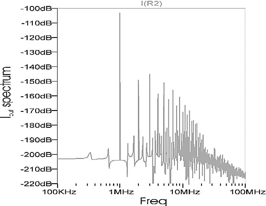
Distortion is introduced mainly by the third harmonic which is 42dB below the fundamental. The total harmonic distortion is close to 1%.

4 Experimental Results

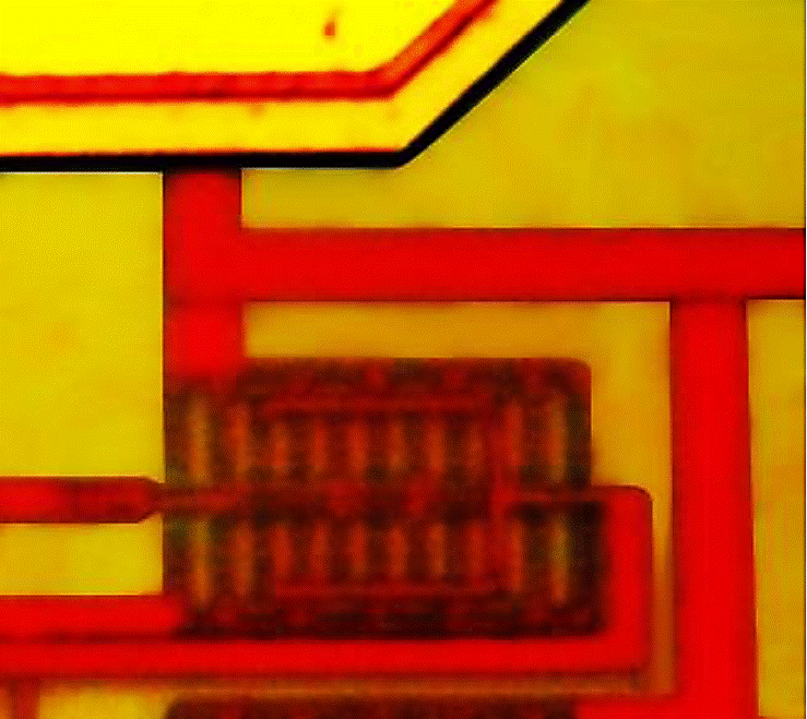
The proposed current mirror was fabricated using 0.5μm CMOS technology. The circuit layout was developed using common centroid techniques and dummy structures in order to improve transistor matching. The microphotograph of the circuit is shown in Fig. 7, and the occupied silicon area was 37μm × 27μm.

Fig. 7 Current mirror microphotograph 

The different tests were performed using a load of 47kΩ to measure the output current by a digital oscilloscope. The input current was introduced using a signal generator and a series resistance of 1MΩ.

In Fig. 8, the circuit was stimulated with an input square signal of 50kHz; the input current was 20μApp and the inverted output current shows a good performance with a 5% error in the copied current.

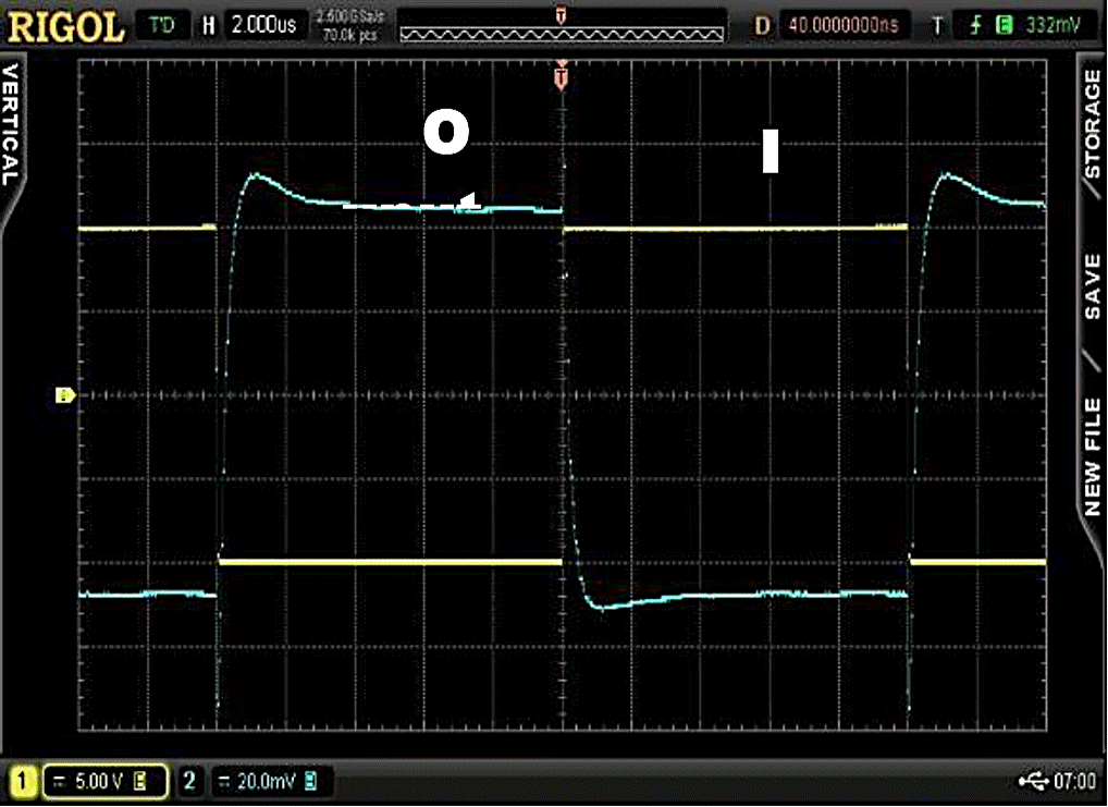
Fig. 8 Input/output traces of the current mirror considering a 1MΩ input series resistance and 47kΩ load resistance 

The spectral response was measured also with 5kΩ load and a sinusoidal input signal of 2μAp@5kHz. The trace is shown in Fig. 9. THD was measured close to the simulations results, this is 1%.

Fig. 9 Current mirror spectral response 

Measurements were performed with VDD=1.5V and 1μA bias currents. Hence, the circuit presents a static power consumption of only 3μW.

In Table 1 a comparison among other approaches is presented, as well know, there is a clear relationship between performance and power consumption. Nevertheless, each circuit has own properties in order to be used for a given application. The circuit proposed could be considered as a good choice for low-power and low complexity applications.

Table 1 Comparison among other CMOS current mirrors 

work 3 4 6 This
Rin 18Ω 15Ω - 15kΩ
Ro 11MΩ 650MΩ - 1MΩ
BW (MHz) 120 100 10 30
Power (μW) consumption 165 264 (30 3
VDD (V) 3.3V 3.3V 1.5V 1.58V
Silicon area 140× 295× - 37×
130μm 75μm 27μm
Transistor Count 17 23 8 4

5 Conclusions

In this work, a very compact and simple lowvoltage, class AB bidirectional current mirror is presented. The circuit can drive currents much larger than its static bias current as shown through simulations and experimental measurements. The circuit has an unconditionally stable behavior due to the existence of only one high impedance node, thus, no compensating passive elements are required.

The simplicity of the circuit makes it feasible for low-power/ low-voltage applications.

References

1. Kawahito, S. & Tadokoro, Y. (1996). CMOS Class-AB Current Mirrors for Precision Current-Mode Analog-Signal-Processing Elements. IEEE Transactions on Circuits and Systems II: Analog and Digital Signal Processing, Vol. 43, No. 12, pp. 843-845. [ Links ]

2. Hassan-Faraji, B. & Seyed-Javad, A. (2011). Very low input impedance low power current mirror. Analog Integrated Circuits and Signal Processing, Vol. 66, No. 1, pp. 9-18. [ Links ]

3. Lopez-Martin, A.J., Ramirez-Angulo, J., Carvajal, R. G., & Algueta, J.M. (2008). Compact class AB CMOS current mirror. Electronics Letters, Vol. 44, No. 23. [ Links ]

4. Esparza-Alfaro, F., Lopez-Martin, A.J., Ramirez-Angulo, J., & Carvajal, R.G. (2012). High-performance micropower class AB current mirror. Electronics Letters , Vol. 48, No. 14. [ Links ]

5. Ramirez-Angulo, J., Carvajal, R.G. & Torralba, A. (2004). Low supply voltage high performance CMOS current mirror with low input and output voltage requirements. IEEE Transactions on Circuits and Systems II: Express Briefs, Vol. 51, No. 3, pp.124-129. [ Links ]

6. Torralba, A., Carvajal, R.G., Jimenez, M., Muñoz, F., & Ramírez-Angulo, J. (2005). A true low voltage class AB current mirror. IEICE Electronics Express, Vol. 2, No.4, pp. 103-107. [ Links ]

7. Ramirez-Angulo, J., Gonzalez-Carvajal, R., Torralba, A., Muñoz, F., Martinez, J., & Tombs, J. (2001). Some techniques for low-voltage continuous-time analog circuit operation. Proceedings of the IEEE 2nd Dallas CAS Workshop on Low Power/Low Voltage Mixed-Signal Circuits and Systems, pp. W90-130. [ Links ]

8. Razavi, B. (2002). Design of Analog CMOS Integrated Circuits. McGraw Hill. [ Links ]

Received: August 10, 2016; Accepted: November 08, 2016

Corresponding author is Ines José Rivera Mejía.

Jesús Ezequiel Molinar Solis received the electronics engineering degree from the Technological Institute from Ciudad Guzman (ITCG), Jalisco, in 1999. He obtained the M. Sc. and Ph. D. degrees in electrical engineering at the Center for Research and Advanced Studies (CINVESTAV-IPN), Mexico City, in 2002 and 2006 respectively. He is currently working as a Research Professor with the Technological Institute from Ciudad Guzman, his research interests are related to analog circuits, neural networks and vision chips.

Humberto Bracamontes del Toro received the B.S. degree in electronics engineering from the Instituto Tecnológico de Cd. Guzmán, México in 1992. The M.S. and Ph.D. degrees were obtained from the École Nationale Supérieure des Télécommunications de Bretagne, Brest, France in 2006. From 1992 to 2001 he has been professor with the Electronics Engineering Department at I.T. Cd. Guzmán. Since 2006 he has been professor with postgraduate electronics and since 2012 he has been the head of graduate studies and research division at I.T. Cd. Guzmán. He research interests include embedded systems design and signal processing for digital communications and remote sensing, smart antenna and multiplexing techniques for high frequency communications.

José Rivera Mejía received the M.Sc. degree in electronics engineering from the Instituto Tecnológico de Chihuahua (ITChih), México in 1979, and Doctorate of Engineering degree from the Universidad Autónoma de Querétaro (UAQ), México in 2008.Dr. Rivera-Mejía is member of the National Researchers System in Mexico. His doctoral dissertation was recognized at the UAQ as the best thesis in 2008. He received the Award of Science and Technology and Innovation in the State of Chihuahua, third place in 2012. His research interests include Intelligent Sensors, Measurement Systems, Metrology and Reliability.

Sergio Sandoval has a degree in Electronics Engineering from the Instituto Tecnológico de Guzmán ITCG (2000). He holds a Master's Degree (2010) in Electronics Engineering from ITCG and a Doctorate (2015) in Sciences with a specialization in Computing and Automation from Cienega University Centre at the University of Guadalajara. He is interested in areas of automation, linear and design of programming methodologies for application to the automobile.

Miguel Rocha Pérez received the B.S. degree in electronics from the Universidad Autónoma de Puebla, Puebla, México in 1986 and the M.Sc. and Ph.D. degrees from the Instituto Nacional de Astrofísica Óptica y Electrónica (INAOE), Puebla, in 1991 and 1999, respectively. During 1991- 1996, he was working on the control of telescopes in the Astrophysics Department, and during 19992001 he was with the Instrumentation Lab at INAOE. He is working at INAOE in the Electronics Department. His current research interests are on the design of integrated circuits for communications and IC implementation of digital algorithms.

Alejandro Díaz-Sánchez received the B.E. from the Madero Technical Institute and the M.Sc. from the National Institute for Astrophysics, Optics and Electronics, both in México, and the Ph.D. in Electrical Engineering from New Mexico State University at Las Cruces, NM. He is actually working as Full Professor at the National Institute for Astrophysics, Optics and Electronics, in Tonantzintla, Mexico. His research concerns analog and digital integrated circuits, high performance computer architectures and signal processing.

Víctor Hugo Ponce Ponce received the degree in Communications and Electronics Engineer from the Mechanical and Electrical Engineering (ESIME) of the National Polytechnic Institute (IPN) in 1993, a Master's Degree in Electrical Engineering and a Doctor of Science in Electrical Engineering at the Center Research and Advanced Studies (CINVESTAV), Campus Cd. Mexico, in 1994 and 2005, respectively. From 2007 to 2008, he held a one-year sabbatical stay at the Polytechnic School of Montréal. He currently a professor at the Computer Research Center of the IPN, attached to the Laboratory of Microtechnology and Embedded Systems. His research interests are currently focused on the Micro Electromechanical Systems (MEMS) in conjunction with signal conditioning circuits an integrated circuit level in CMOS technology.

Creative Commons License This is an open-access article distributed under the terms of the Creative Commons Attribution License