


 nueva página del texto (beta)
 Inglés (pdf)
 Artículo en XML
 Referencias del artículo
 Enviar artículo por email
 Citado por SciELO
  Similares en
SciELO
Similares en
SciELO 
 Permalink
1 Introduction
Thin film solar cells of the CdS/CdTe type are considered an excellent choice for photovoltaic (PV) conversion and large-scale production of PV modules based on this technology because of their simplicity, low processing cost and good results [1]. Technological applications that require a 3.3 V supply and an average power of only a few tens of μV with a maximum power of tens of mW, are of interest for the use of PV solar cells. These include intermittent wireless remote sensors, hotel door locks, industrial controls, alarms, data transfer systems, etc. A solar panel system is composed of a battery, battery charger and voltage converter. The technological demand for these systems is immense and therefore, it is a good opportunity for the application of mini-modules, leaving aside the use of conventional batteries.
First Solar Inc. is a leader in cadmium tellurium (CdTe) thin film PV modules processing, with a photovoltaic efficiency record of 18.6 ± 0.5 % [2]. This company reports 450 MW/year by using GEN 6 SERIES modules of 1500 ×1800 mm with thicknesses around (∼1-3 μm) with a total manufacturing cost of $ 0.4/W in MSP (minimum sustainable pricing) [3]. Antec Solar and Calyxo Company produce CdTe modules with maximum powers of 60 and 110 W respectively [4- 5].
The PV efficiency and electrical stability of CdTe PV modules depend on the production process and material properties. CdTe thin films with a 1 μm of thickness can absorb 90% of the incident light because of their high absorption coefficient (>105 cm-1) [6]. The theoretical solar energy conversion efficiency of CdTe PV devices is approximately 28% [7]. On the other hand, CdTe modules have an average life-time of 20 - 30 years, depending on the physical properties of the window and absorbent materials used and the deposition techniques [4]. The PV response of CdTe modules depends on the assembly, solar irradiation, module temperature and other weather conditions [8- 9].
Numerous efforts have been reported to improve the PV- efficiency in large CdTe modules because increasing the effective area, open circuit voltage (Voc) and fill factor (FF) are reduced. The PV-performance of CdTe modules can be improved by employing a laser scribing technique for electrical interconnections [10- 12].
Run Luo et al.[13] reported a CdTe solar cell by using the following structure: glass/FTO/CdS/CdTe/graphite slurry/Au; CdTe thin films in areas of 30×40 cm were used as absorbent material, a PV efficiency of 14.6 %, a short-circuit current density (Jsc) of 26.9 mA/cm2, open-circuit voltage (Voc) of 823 mV and fill factor (FF) of 66.05 %.
R. Mendoza et al. [14] reported a CdTe PV module consisting of nine solar cells with approximately 3 cm2 of contact area. At least six cells have the same I-V characteristics in the dark as well as illumination AM1.5 (100 mW/cm2), having a maximum efficiency value of 5.8 % with a J J sc of 16.4 mA/cm2, a Voc of 640 mV and an FF of 57 %.
The aim of this work is to develop different CdTe mini photovoltaic (PV-M) modules in areas of 40 cm2 employing a low cost of processing and studying its electrical parameters under outdoor conditions. For this purpose, CdS and CdTe thin films were carried out in areas of 40 cm2 and used as window and absorbent materials in the PV-M development. In order to study the electrical interconnections, two PV-M were developed the first one was sectioned into five regions (R1 to R5) and the second one was conformed by 14 cells interconnected in series by laser scribing with an effective area of 29 cm2. Finally, two PV-M conformed by 14 cells were connected in series and their photovoltaic performance to CDMX, México were studied under outdoor conditions considering different day hours and different charge conditions.
2 Experimental details
2.1 Thin films growth
CdS thin films were deposited on SnO2:F (FTO) substrates using the Chemical Bath Deposition (CBD) technique. The chemicals CdCl2 (0.12M), NH4Cl (0.2M), NH2 (2M) and thiourea (0.3M) were used as precursor solutions, the deposition time was 12 min at 70 °C. The CdS films were thermally annealed in air for 60 min at 450°C. On the other hand, CdTe thin films were grown by the Close Space Sublimation (CSS) technique considering different growth parameters such as source (Tf) and substrate (Ts) temperatures, respectively. CdTe thin films were thermally treated in CdCl2 at 350 °C for 3 min. The specific deposition parameters were reported in Table I.
Table I Growth parameters of CdTe thin films in 40 cm2.
| Sample | Tf (°C) | Ts (°C) | Pressure (mTorr) |
|---|---|---|---|
| CdTe1 | 590 | 400 | 100 |
| CdTe2 | 600 | 450 | 100 |
| CdTe3 | 600 | 430 | 150 |
| CdTe4 | 590 | 400 | 150 |
| CdTe5 | 600 | 430 | 200 |
Polycrystalline structures of all samples were determined by grazing incidence X-ray diffraction (GI-XRD) at 0.5° using the CuKα line in a Rigaku Smart Lab system. The thicknesses of the films were obtained using a profilometer Ambios Technology XP-100. The surface morphology, grain size and elemental analysis (EDS) were performed using a Bruker System coupled with a Scanning Electron Microscope (SEM) model Auriga-Zeiss with an acceleration voltage of 5 kV and 10 kV. AFM images were obtained in contact mode using NP-10 Bruker AFM probes with the Atomic Force Microscope Innova Veeco. The Band gap values of the samples were determined by Photoacoustic Spectroscopy technique (PAS), where a ConerStone C130 grating monochromator coupled to a Xenon lamp (1000 W) as the light source was used; the light was modulated with a fixed frequency at 18 Hz using a New Focus 3502 Phase Locked Optical Chopper.
An electret microphone on close photoacoustic cell is used to detect photoacoustic signal (amplitude and phase) using a Stanford Research SR850 lock-in amplifier. Photovoltaic effect (PV) was performed by Sol3A Class AAA Solar simulator equipment with a light source of 100 mW/cm2 (AM1.5).
2.2 CdTe PV-M manufacture
CdTe PV-M (40 cm2) was manufactured with the purpose of evaluating the electrical parameters influenced by the electrical interconnection (see Figure 1a)).
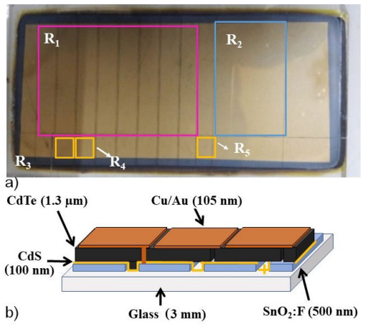
Figure 1 a) CdTe PV-M (A) considering R2, R3, R3 and R5 without electrical interconnection and R1 conformed by 8 cells in series interconnection b) Detail of the electrical interconnection.
All PV-Ms were developed in the following arrangement FTO/CdS/CdTe/Cu/Au. The first one (A), was sectioned into five regions, region R1 corresponds to eight interconnected cells with an effective area of 13.35 cm2 and R2 non-interconnected cell with an effective area of 1.4 cm2. These regions were prepared to analyze the electrical interconnections on the electrical response. Regions R3, R4 and R5 were separated to study the electrical parameters in smaller areas (0.3 cm2). The metal back contacts were evaporated by thermal evaporation technique with thicknesses of approximately 5 nm of Copper (Cu) and 100 nm of Gold (Au), and additional thermal treatment at 200 °C for 20 min was performed.

The interconnection of the cells was made by laser scribing in three sequential stages as reported by H. Lai et al[15], (Fig. 1b)).
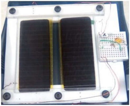
CdTe PV-M (B) with area of 40 cm2 was processed and it was conformed by 14 interconnected solar cells in series; The electrical interconnection was made by using a laser scribing technique, with a contact area of 29.4 cm2.
3 Results
This section shows the results of Morphological, structural, optical and electrical characterization of the materials that were synthetized by CdS and CdTe modules PV-M.
Table I shows different deposit conditions such as the source temperature (Tf) and substrate (Ts). For all the CdTe thin films, a deposition time of 20 min was used in atmosphere of Oxygen (50 %) and Argon (50 %).
3.1 Characterization of CdS and CdTe thin films in large area
3.1.1 Morphological properties of CdS and CdTe thin films
Scanning electron microscopy (SEM) and Atomic force microscopy (AFM) analyses allowed us to visualize and analyze the surface morphology and topography of the CdS and CdTe thin films. Figure 4, shows SEM micrographs of CdS thin film, which reveals a compact and homogeneous nanocrystalline structure composed of spherically shaped clusters, which are distributed over the entire surface of the substrate.

In addition, it is possible to observe the shape of the possible crystals with well-defined faces in the CdS matrix, which was related to cadmium oxide crystals as an n-type semiconductor with a cubic crystalline structure. This is a material with high optical transparency in almost the entire electromagnetic spectrum with a direct band energy with reported values between 2.18-2.5 eV, it has a resistivity of ∼5 × 10⁻¹ Ω-cm and a high mobility of holes, which make it a material that is beneficial to be part of the device due to the physical properties it present. This material could be identified in the GI-XRD spectrum, and it should be noted that these micrographs (Fig. 4b)). Also, this analysis was done in the samples with heating treatment at 450 °C in air atmosphere for 1 h.
Morphology, grain size, thickness and grain boundaries have a significant impact on the physical properties of CdTe and on the PV performance of CdS/CdTe PV-M. In Figures 5b and 5h, which correspond to the CdTe1 and CdTe4 films show a granular growth in the form of a stack with well-defined facets on a uniform surface. The grain sizes were measured in a range of 1.5 to 2 μm. Figure 5h has a more uniform and consistent grain growth with a decrease in grain size of approximately 1 μm with an adequate base this decrease in grain size can be attributed to the increase in pressure during the deposit of thin film modifying growth kinetics. CdTe3 y CdTe5 thin films were deposited with the same temperature gradient and with an increase in pressure from 150 to 200 mTorr. Figures 5f) and 5j), show pressure influence on CdTe grains growth; due to grains are not well defined. An important growth parameter is pressure because it modifies the CdTe morphological properties.
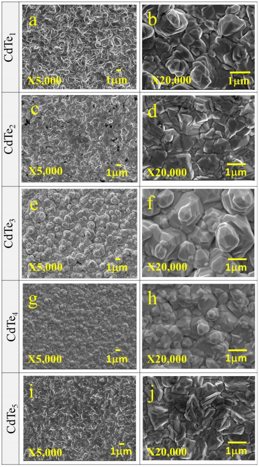
The CdTe2 sample showed an uniform growth without cracks or pores; however, the grain size was uneven with an average grain size of 1 mm, and the grain borders were inconsistent, presenting a growth similar to that of CdTe5 sample. All the CdTe thin films were deposited using different growth parameters with respect to temperature and pressure. As shown in Figs. 5a, 5c, 5e, 5g and 5i with uniform and compact growth.
The Energy Dispersive X-ray Spectroscopy (EDXS) analysis was used to determine the elemental composition of the CdS thin films. The semiquantification of elements reported in shows the atomic percentages of the elements of interest, in the case of CdS a semi-quantitative analysis, with an excess of Cd, around 64 %, which is known that sulfur vacancies are common defects in CdS thin films that give it n-type conductivity. To determine the elemental composition of the crystals that appeared on the CdS surface.
Table II Chemical composition of CdS thin films.
| Atomic (%) ± 3% | |||
|---|---|---|---|
| Sample | Cd | S | O |
| CdS | 64 | 36 | - |
| CdO grains | 43 | 18 | 39 |
A punctual EDXS analysis was applied, and no signal corresponding to tin (Sn) was detected on the crystals, so oxygen does not correspond to the conductive substrate FTO and could be related to Cd by having only a small amount of S, and the O/Cd ratio was almost stoichiometric. This suggests that the crystals observed on the surface of CdS correspond to a material that contains bonded Cd and S, such as CdO crystals.
Table III shows the semi-quantitative analysis of the elements present, as well as the grain sizes and the thicknesses of the CdTe films. Cadmium vacancies provide this semiconductor material with p-type conductivity. On the other hand, when comparing the samples CdTe1 with CdTe4 and CdTe3 with CdTe5, it was observed that both the thickness and the grain size decreased with increasing deposit pressure.
Table III Chemical composition of CdTe thin films.
| Samples | Thickness (μm) |
Average Grain Size (μm) |
Atomic (%) ±3% |
|
|---|---|---|---|---|
| %Cd | %Te | |||
| CdTe1 | 2.5 | ∼1.5 | 50 | 50 |
| CdTe2 | 2.5 | 1 | 50 | 49 |
| CdTe3 | 2.5 | 2 | 48 | 52 |
| CdTe4 | 1.5 | 1 | 48 | 52 |
| CdTe5 | 1.5 | 1 | 50 | 49 |
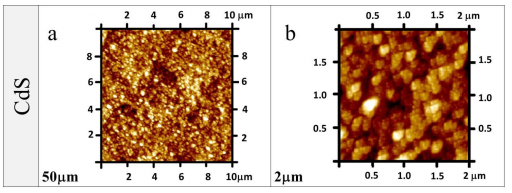
Figure 6, AFM shows images of the CdS thin film deposited by the shallow chemical bath technique; in these images we can appreciate the morphological properties of the sample. The morphology of CdS thin film is influenced by the deposit conditions and the system used in the CBD. Presenting a morphological growth with some roughness and longitudinal caverns along the surface of the CdS, these caverns could not be seen in the SEM images. However, these caverns do not reach the base of the transparent conductive oxide (FTO), so this type of film has a morphology with certain defects that can be beneficial to be applied as a window material in solar cells of the CdS/CdTe type.
To study the surface characteristics of CdTe thin films it is necessary to characterize their surface morphology. Figure 7 shows AFM images corresponding to square scanning they are grouped for each of the samples of 10 × 10 μm and 3D images, in order to show the topography in detail.

Figures 7b), 7d), 7f), and 7h) show a growth of the grains with stacking and volumetric defects of twins, as shown in Fig. 5b) a grain size of 2 μm was observed. Figure 7a) and 7g) show a grain size decrease due to pressure increment, On the other hand, an increment on temperature growth parameters modify the morphology on CdTe surface increasing the grains boundaries (see Figs. 7a) and 7c)). Using source and substrate temperature about 600°C and 43 °C respectively with different pressures conditions could modify the morphological properties from bidimensional to tridimensional growth (see Figs. 7e), 7f), 7i) and 7j)).
CdTe uniform thin films with grains well defined and less grain boundaries are required to develop efficient photovoltaic solar cells. According with AFM results CdTe1 and CdTe3 (see Figs. 7a), 7b), 7e) and 7f)) could be used for this porpoise.
3.1.2 Structural properties of CdS and CdTe thin films in large area
The GI-XRD diffraction pattern of CdS shown in Fig. 8 shows, the polycrystalline nature of the thin film, which exhibits a diffraction peak of greater intensity at 2θ = 26.6°, which coincides with the (002) diffraction plane of the hexagonal crystalline phase (wurtzite) of CdS. This peak is very pronounced and narrow, indicating the polycrystalline quality of CdS. In this work, thin films of CdS with a hexagonal crystalline structure with a diffraction peak of greater intensity at 2θ = 51.6°, which corresponds to the diffraction plane (112). In the same way as in Fig. 8 we observed diffraction peaks of less intensity than the reported in the literature corresponding to the orientations (100), (101) and (112) to the hexagonal phase, which were identified according to the crystallographic chart PDF # 41-1049. It was also possible to identify diffraction planes corresponding to the SnO2 tetragonal phase and diffraction planes corresponding to cubic cadmium oxide (CdO), using PDF # 41-1445 and PDF # 05- 0640 respectively.

Figure 9 shows the GI-XRD diffractograms of CdTe thin films. The peaks that appear in each samples were indexed using the crystallographic chart PDF # 15-0770, when comparing the diffraction patterns with the modeled diffraction pattern for the CdTe, a correct correspondence is observed, showing characteristic planes of the cubic structure with a preferential orientation in the plane (111), in addition characteristic diffraction planes can be observed in directions (220), (311), (400), (331), (422) and (511) corresponding to the cubic phase. An analysis was carried out from 20 to 80° in the 2θ position, for indexing the peaks or maxima corresponding to diffraction modeling CdTe. Moreover, the CdTe2 sample shows more symmetric peaks with less dispersion, which indicates that it exhibits greater crystalline perfection, compared to the other samples.

3.1.3 Optical properties of CdS and CdTe thin films
Photoacoustic spectroscopy (PAS) provides the possibility of determining the optical absorption coefficient spectra of thin film semiconductors from their photoacoustic amplitude spectra and can be used for calculations of the semiconductor band gap energy (E g ) using the TAUC method as support. In Figs. 9 and 10, CdS and CdTe thin films PAS spectra are shown at different frequencies and characteristic wavelengths for each material.
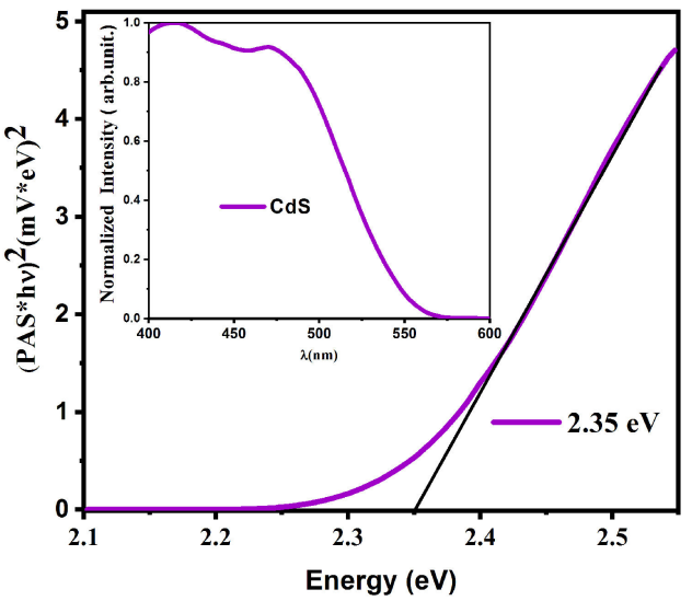
To calculate the E g value of the PAS spectra, it can be seen thin films are thermally stable and the coefficient of thermal diffusion of the samples is
where β is the thermal diffusion coefficient of the films, and f is the modulation frequency of the chopper, in this case these satisfies the TAUC ratio, where
The band gap energy was determined by plotting α 2 v/s hν and then extrapolating the straight-line portion to the energy axis. Thus, we can estimate the band gap energy (E g ) according to the model for allowed direct transitions (2) and the square of the PAS signal.
In Figs. 10 and 11, the square of the PAS signal vs photon energy (eV) is plotted for the CdS and CdTe thin films, to determine the band gap energy of the thin films. We found band gap values of 2.35 and 1.43 eV respectively. These values are similar to those reported in the literature, therefore these materials present values of the band gap energy suitable for their application in solar cells.

3.1.4 Electrical properties
The electrical properties of CdS thin films were obtained using the four-point technique, obtaining an average value of 3.4 × 10³ Ω-cm. Profilometric measurements, were performed in different areas of the thin film surfaces, obtaining average thickness values of 0.09 μm.
The same technique was used to determine the resistivity and laminar resistance of the thin CdTe films. In Fig. 12, it is observed that the resistivity values are in the range of 105 Ω -cm, which is the approximate value reported for this material.


3.2 CdS/CdTe mini-module current-voltage characterization
PV-M∼s and C type were manufactured at 40 cm2, using the CdS film and the CdTe3 film, which have the best morphological, structural, optical and electrical properties. During processing, serial interconnection was carried out using the laser scribing technique. PV-M (A) (see Fig. 1a)) was sectioned into five regions with different areas by manual scratching; where R 1 consists of eight cells interconnected in series with an effective total area of 13.35 cm2, R 2 is a cell without interconnection with an effective area of 1.4 cm2 and finally the R 3, R 4 and R 5 regions, which are isolated cells with an effective area of 0.3 cm2. The last three regions were considered to evaluate the photovoltaic response in different sections of this mini-module. The PV-M (A) was sectioned, to evaluate the electrical parameters influenced by the interconnection, as well as to determine whether the interconnection improves or affects the efficiency of this mini-module. In Table IV it is observed the electrical parameters of PV-M (A) and their different regions.
Table IV Electrical parameters determined in different regions of the PV-M (A).
| Region | Area (cm) | Voc (V) | Jsc (mA/cm2) | I (mA) | FF (%) | η (%) |
|---|---|---|---|---|---|---|
| R1 | 13.35 | 5.06 | - | 2.38 | 0.39 | 4.7 |
| R2 | 1.4 | 0.62 | 9.66 | - | 0.26 | 1.6 |
| R3 | 0.3 | 0.69 | 22.17 | - | 0.51 | 7.9 |
| R4 | 0.3 | 0.68 | 22.54 | - | 0.44 | 6.8 |
| R5 | 0.3 | 0.61 | 20.90 | - | 0.43 | 5.6 |

Comparing region R 1 with region R 2 the series interconnection improves the efficiency of the module because, submodule R 1 has a greater contact area and its efficiency value is 4.7 % compared to R 2 solar cell with its area is 1.4 cm2 and efficiency of 1.6 %. According to these results, PV-M (B) (see Fig. 2) was manufactured using 14 cells interconnected in series, with a contact area of 29.4 cm2 and its electrical parameters were analyzed.
On the other hand, the isolated cells presented efficiencies for R 3, R 4 and R 5, obtaining efficiencies of 7.9, 6.8 and 5.6 %, respectively. Otherwise, region R 1 has a higher V oc than the others regions but the value of J sc decreases, in the case of region R 2 which does not present interconnection, the value of V oc decreases drastically and the current density increases compared to R 1, for individual regions, its to say R 3,R 4 and R 5, the J sc value and decrease the value of V oc . With this it is observed that the serial interconnection improves the efficiency of the module, because by delimiting and indicating the area through which the electrons must flow, the efficiency increases and decreases the losses due to recombination.
3.3 Performance of a CdS / CdTe minimodule under different load and irradiance conditions
To evaluate, the performance of the mini-modules developed, it is essential to analyze their electrical behavior under different load and external irradiance conditions.
Considering the zenith angle of sun rays is the same for all modules along the day. Comparing the current values for the PV-M (B) mini-module analyzed under simulator (AM1.5) respect the daily hours it can see a variation of these values from 18 mA to 27 mA obtaining the maximum value at 12:20 hours (see Fig. 15). In this way the influence of the temperature on the mini-module performance was not studied; however, it contributed on stability.
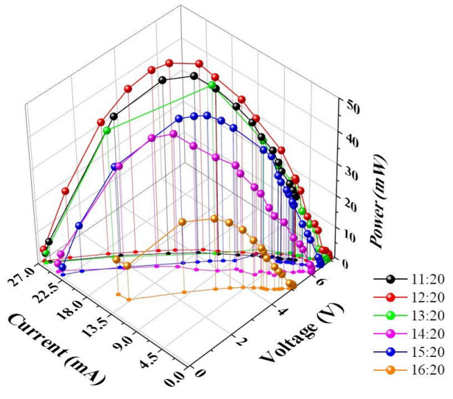
After analyzing one mini-module of 40 cm2, two PV-M (B) were connected in series to observe the performance under different load conditions at different day hours (see Fig. 16).

In this case, maximum power is obtained at midday (zenith highest point), this power decreases as the irradiance decreases. The current density is maintained, and the voltage increases significantly, which indicates adequate electrical response of these devices. A linear dependence has been observed between the power and irradiance along the day. Figures 17a) and 17b) show two PV-M (B) of 40 cm2 connected in series powering 24 LEDs arrangement. In summary, the results show that the efficiency and performance of the mini-modules in outdoor conditions depend on the solar radiation.

4 Conclusions
CdTe and CdS thin films were grown in areas of 40 cm2 with homogeneity, the samples were analyzed in different regions. A CdTe PV-M were developed using two techniques CBD and CSS, which are low-cost techniques. The laser scribing technique was implemented in CdTe and CdS thin films satisfactory, which allowed the interconnection of all thin films to collect more carriers in all cells increasing the current. The CdTe mini-modules performance were analyzed under different outdoor conditions, observing stable behavior with different solar radiation. CdTe PV-M allow turning on 24 green LEDs connected in series and shut configuration.

