


 nova página do texto(beta)
 Inglês (pdf)
 Artigo em XML
 Referências do artigo
 Enviar este artigo por email
 Citado por SciELO
  Similares em
SciELO
Similares em
SciELO 
 Permalink
Introduction
At of the time of writing, more than 250 million people have been infected and more than 5 million deaths have been reported since the pandemic related to new Severe Acute Respiratory Syndrome Coronavirus (SARS-CoV-2) began [1]; however, the problem is more serious than it seems. More than 37 million HIV patients and their treatment are at risk [2], just like the attention for noncommunicable diseases such as hypertension, and cardiovascular emergencies, diabetes and its related complications, even cancer patients [3-5] which were partially or completely diminished to dedicate the best efforts as possible to Coronavirus Disease named COVID-19. This situation has been triggered by the lack of staff strongly related to workers’ reassignment, medicine shortage, and a decrease in public transport services [6].
From another perspective, stay-at-home policy and social distancing have brought consequences in mental health such as depression and anxiety [7,8], even changing the perception of safety and security. Only the North America and Russia-Eurasia regions (2 out of 9 regions in the world) became more peaceful in comparison with 2019. This means that shocks like COVID-19 and the resulting recession have affected education, societal safety, security, as well as the domestic economy, especially in the more vulnerable and conflicting regions [9].
According to a report from the Institute of Economy and Peace, global violence has cost around USD 14,528.9 billion in Purchasing Parity Power terms in 2019 [10]. Thus, the following scenario is not promising while violence continues to increase. Moreover, at least 88 million people could fall into extreme poverty at the end of 2020 and up to 35 million more in 2021, indicating a three-year reversal of world prosperity and fight against poverty [10]. This increase in poverty is largely due to the fact that most of the people who work in the informal sector without social security have been affected by mobility restrictions, social distancing, and lockdowns [10].
When people worldwide began to need some protection to continue their ordinary life during the SARS-CoV2 outbreak, some products got more expensive and inevitably inaccessible. At this point, also the World Health Organization (WHO) published recommendations about what barriers and personal protection equipment were useful to diminish the number of deaths and seriously ills [11]. These recommendations provoked the facemask and respirators market into an increment from USD 1.03 billion (before the outbreak) to more than USD 2.5 billion at the end of 2020, reaching up to USD 2.8 billion in 2026, depending on the pandemic evolution [12], and the overprices that, in some cases, have reached a factor of five [13]. As a consequence, both the production and the pollution related to these have increased up to more than 20 times from February to June 2020 [14].
To meet the demand and overprices, elaboration of homemade masks and reuse of standardized ones have been taken as two options; however, the reuse of equipment exposed to pathogens may cause a considerable increment in confirmed cases by reduction of effectiveness [15]. A review of diverse disinfection approaches points to UV radiation as a useful and effective disinfection method to face the SARS-CoV-2 spread and the COVID-19 contagion. Fighting the pandemic by a disinfection approach will contribute to reduce social distancing and restart activities such as commerce, tourism, and education, which will counteract the side effects on mental health, security, and the economy. On the other side, facemasks costs might be reduced while the demand for disposable Personal protective Equipment (PPE) is reduced from the reliable reuse of disposable medical gowns, facemasks, and respirators.
Despite Light Emitting Diode (LED) technology being closely related to electronic devices development in different areas such as lighting [16], communications, and entertainment, a growing interest is showing up in healthcare to generate faster and more accurate tools (e.g., medical equipment, vital signs monitoring devices, disinfection, sensors) [17,18]. Due to the recent health crisis in the world, special efforts on disinfection research have been made to obtain and optimize barrier mechanisms avoiding infectious agents like SARSCoV-2 [19], MERS-CoV [20], and Ebola [21]. Although Low-Pressure Mercury (LPM) lamps and, still in development, UVC LED devices (200-280 nm) are effective against viruses and bacteria [22], material research and deposition techniques are widely studied because of deoxyribonucleic acid (DNA) and ribonucleic acid (RNA) destructive properties of UVC radiation [19, 23, 24]. Is important to mention that LPM lamps have characteristics that put them at disadvantage compared to UVC LEDs (e.g., big size, fragile glass components, usage of Hg, and shorter lifetime). However, it is still necessary that LEDs increase their power levels and enhance their efficiency in order to reduce exposure time achieving the same disinfection effectiveness [23, 25]. One of the most important issues to deal with is the fact that, as the wavelength emission shortens, the device shows less power [26]. Therefore, is essential to determine the optimal wavelength for the device design [26, 27] considering short exposure times, since as the exposition time increases the UV disinfection could be counterproductive [28]. Fortunately, UVC-LEDs are still being improved and efficiency is expected to increase so that this technology substitutes the LPM lamps for UV disinfection. In order to unfold the challenges and drawbacks in the development of UVC-LED based on III-nitrides, it is important to approach the fact that disinfection requires UVC range emissions to inactivate viruses.
Virus inactivation mechanism
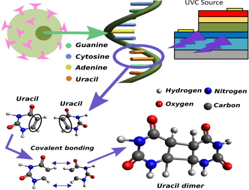
The spread of diseases and the capability of human beings to endure infections are susceptible to the amount of infectious load to which we are regularly exposed. It is remarkable to mention that different environments refer us to different viruses and bacteria loads [29], which inevitably puts human life at risk for disease contagion. Viruses depend on a host to maintain activity and reproduce; thus, they have to adhere to a cell that allows them to continue transmitting their genetic information. This is encoded as a sequence of nucleotides, which are made up of nitrogenous bases linked to deoxyribose or ribose in DNA or RNA, respectively [30]. The nitrogenous bases that are part of DNA are Guanine-CytosineAdenine-Thymine, while in RNA Uracil replaces Thymine. Using the machinery of the cell, the nucleic acid (DNA or RNA) of the virus produces proteins through a mechanism that involves messenger RNA (mRNA). These proteins function as antigens that stimulate an immune response in the body [31,32]. The mRNA is decoded and used for designing vaccines to face the COVID-19 pandemic [33]; however, the challenge of delivering the artificial mRNA to the cells (either naked mRNA in vivo or wrapping it with lipid-based carriers) remains [34]. While pharmaceutics and researchers are looking to diminish both contagion and disease symptoms, it is also necessary to consider different approaches (inactivated or attenuated virus, replication vectors, RNA or DNA, among others) [35] and the side effects (from fatigue, pain, chills and skin reactions to fever, urinary retention, and even moderate Bell’s palsy) 31 to guarantee vaccine safety [36]. On the other hand, RNA-based viruses show rapid mutation compared to DNA-based viruses [37]; thus, SARS-CoV-2 mutations result in more infectious virus strains that could complicate the vaccine development and efficiency [38,39].
UV radiation for disinfection
While the development of vaccines and treatment against SARS-CoV-2 and COVID-19 continues its progress [36], it is reliable to aim at disinfection as a mechanism to prevent contagion [28]. In contrast with vaccine effectivity, UV disinfection is not affected by virus mutations due to the fact that the effectiveness of UVC devices on coronaviruses inactivation is based on the formation of dimers by adjacent uracil or thymine present in RNA or DNA, respectively. This genetic disruption mechanism is triggered by photoreactions and is due to the sensitivity of these nitrogenous bases to UVC radiation [40,41]. First, the photons emitted around 260 nm are absorbed by the nitrogen bases breaking a specific carbon covalent bond in the ring of the molecule (as shown in Fig. 1) so, at this moment, the two adjacent bases are linked through stronger covalent bonds provoking genetic mutation by chain disruptions [22,40,41]. Because of this RNA (DNA) sequence’s fractures, the capabilities of viruses and bacteria are depleted, preventing their lodging, reproduction, and the infection that causes to the host [42]. Therefore, the use of germicidal UVC radiation devices to disinfect potentially infectious surfaces is taken as an important object of study to compare efficiency, risks, and benefits between technologies [27,43,44]. It is possible to disinfect surfaces such as walls and furniture inside hospital rooms [45], even N95 masks and PPE achieving a 90% inactivation of viruses, making possible their reuse [46]. Nevertheless, it is crucial to determine the correct dose with minimal damage to filtering facepiece respirators [47], considering that the longer wavelength is, the higher the used dose must be [26]. Some complementary treatments or disinfections techniques include both UVA and UVC radiation to minimize the risk of contagion. First, UVA (315-400 nm) is used for the reactivation of viruses and bacteria which sequences had been disrupted. Then, a UVC stage is in charge of destroying the most microorganisms as possible by dimerization of thymine or uracil; whatever the case, the experiments are typically performed with Medium Pressure and Low-Pressure Mercury lamps as UVA and UVC sources, respectively [48], increasing the risks of poisoning due to accidental contact with Hg. In the first instance LPM, as the main source of UVC light, has been replaced by its analog LED. Although LEDs emit in narrower bandwidths, these can be set in principle to any wavelength depending on the material.
UV LEDs have their origins in Gallium Nitride (GaN) [49], which allows them to be grown as crystal thin films, reducing dimensions compared to other light sources such as incandescent bulbs or fluorescent lamps. However, these LEDs are limited by the wavelengths available in GaN structures (over 350 nm). In this case, it leaves aside the idea of using it in UVC development. Therefore, the incorporation of aluminum (Al) to attain shorter wavelengths and cover almost the entire UVC range, has been investigated by using aluminum-gallium nitride (AlGaN) alloys [50].
AlGaN-based UV LED
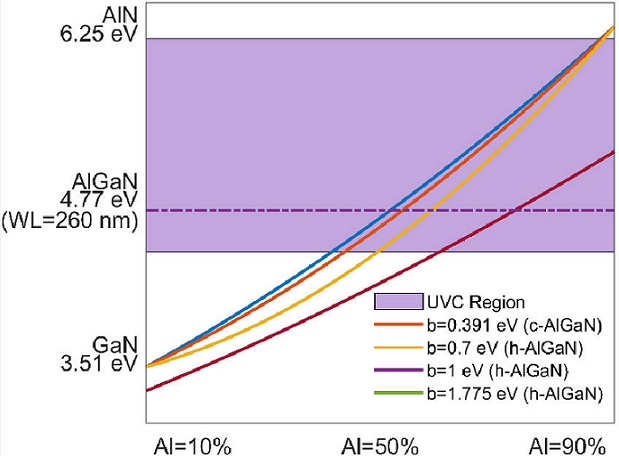
III-N semiconductors are widely studied for LED fabrication, from gallium nitride (GaN) to ternary alloys such as aluminum-gallium nitride (AlGaN) and indium-gallium nitride (InGaN) [51-55]. All these materials have different optical, morphological, and electrical properties which extend their use to different fields. The hexagonal (h) structure is the stable phase of III-nitrides, but the cubic (c) phase (metastable) has also been studied due to distinct properties that we will discuss below. In order to produce a lightemitting device in the UVC range, the energy gap (E g ) of the material must emit photons with energy between 4.43 and 6.20 eV. Thus, from the fact that the range of the AlGaN energy gap extends from 3.27 and 3.47 eV [56] (for c-GaN and h-GaN, respectively) to 5.7 and 6.25 eV [56] (for c-AlN and h-AlN, respectively), and that the bandgap is directly related to Al content [57], E g can be varied by increasing (or decreasing) the Al content according to Eq. (1) [58].
To estimate the alloy’s E g , for the hexagonal phase, it is important to mention that despite early works point to b = 1 eV as a correct value [59], the bowing parameter was also taken as b = 0.7 eV to reduce deviations [60]. However, from more recent work, b in Eq. (1) can be set as 1.775 eV for hexagonal phase, and 0.391 eV for cubic phase [56]. Fig. 2 illustrates the change of E g as a function of Al, it also shows how the bowing parameter affects the expected Eg of the AlGaN alloy. Furthermore, it is important to mention that LEDs are evaluated by their External Quantum Efficiency (EQE), which involves Internal Quantum Efficiency (IQE), Light Extraction Efficiency (LEE), and Carrier Injection Efficiency (CIE), which are related through the Eq. (2) [61].
In order to obtain high-power and efficient UVC LED, three general aspects from Eq. (2) should be considered: first, to enhance the CIE by increasing carrier injection to the active region [62, 63] and preventing the carrier leakage [64,65]. Second, in order to reach higher IQE, it is necessary to diminish the dislocations present in III-N semiconductor [66,67] and, in the case of the hexagonal phase, reduce the effects of strong piezoelectric and spontaneous polarization [68]. And third, the LEE is increased by employing different approaches from patterned substrates to photonic crystals [69-72]. In all cases, it is essential to consider that, while wavelength increases, i.e., from 267 to 297 nm, this shifting provokes an increase in UVC doses required for disinfection of around 26 mJ/cm2 [26].
LED structure considerations
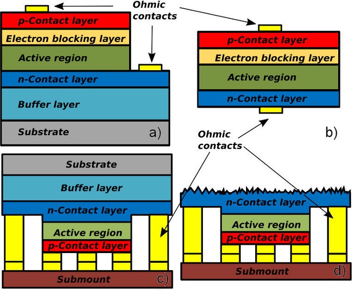
Recently, the use of GaN as the contact layer remains in UVC LEDs design, mostly due to some considerations about doping and transparency that will be mentioned in more detail in later sections. However, the p-contact layer is not the only stage in UVC LED development that could be designed from different approaches. There are superlattices as strain absorber [73] and extra layers [74] that benefit the carrier injection without sacrificing the carrier densities, even carrier blocking layers [75-77] with different structures to prevent the leakage [78].
The typically used LED structures are shown in Fig. 3 in order to visualize the different stages of LED development. In general, the design starts with the substrate and its corresponding buffer layer, the n-type contact layer, the active region, the electron blocking layer, and the p-type contact layer. However, sometimes additional p-type layer is grown to avoid unwanted effects of the p-AlGaN contact layer [79]. Each layer carries diverse challenges [52]: the substrate and its buffer must provide the least number of defects, be as transparent as possible, and allow heat extraction. The ntype layer must spread the current efficiently and manage the strain; the active region faces the main task of increase IQE and carrier confinement which allows emitting photons by energy quantization, and the p-type layer, must enhance the CIE. Thus, it is needed a low resistance in both layers and contacts.
Substrate and buffer layer
The first element to consider is the substrate, here it is very important to choose the appropriate crystal structure since there are relevant differences between the cubic and hexagonal phases of III-N materials [56]. It is important to note that the maximum concentration of Al that the cubic phase allows before the material shifts from direct to indirect bandgap is around 70% [56]. This is a severe drawback because when a semiconductor changes to an indirect bandgap, the probability of radiative recombination is reduced because a phonon is necessary to conserve momentum in the emission of a photon [80]. On the other hand, the hexagonal phase of AlGaN presents the advantage over the cubic phase of requiring a lower concentration of Al to reach higher E g ; nonetheless, when working with h-AlGaN, it is very important to consider that built-in internal electric fields cause a large shift to lessenergetic emission [80], as will be discussed in the next sections. In general, due to the fact that the hexagonal structure is the stable phase of III-nitrides, the state of art unfolds studies that support sapphire as the main substrate in UVC LED growth [74,81-87].
Even though, it is important to consider that crystalline sapphire or silicon carbide films (SiC) still suffer from excessive defects from substrate-film mismatches as thickness increases [88]. This is provoked, to a large extent, by the different lattice constants between the alloy components (AlN, InN, and GaN) [57, 89-91] and the change in the target Al content throughout the multilayer [92]. Moreover, due to its absorption, SiC is not explored enough [93], although, in order to face this drawback, UVC LED on SiC could be processed into a thin-film flip-chip to obtain high LEE [93].
During the growing procedure, these defects introduce nonradiative recombination centers in the semiconductor, which contribute significantly to the reduction of LED efficiency [94]. In other words, the radiative recombination, which is required to emit photons, is limited by dislocations or defects in each layer during their growth affecting both the EQE and the Light-Output Power (LOP) as shown in Figs. 4a y 4b, respectively. Thus, dislocation densities of 109 cm−2 are needed to reach 50% or higher IQE [95]. The state of art reports that nanopattern sapphire substrates show a 98% increase in EQE by reducing the number of dislocations compared to flat sapphire substrates [96]. Another consideration is required since III-V alloy components have different lattice constants; therefore, an AlN buffer layer must be grown to replicate the substrate structure in order to avoid cracks and reduce dislocations [97]. The following layer on the hexagonal AlN must be designed to improve the LED technology and its efficiency [98].
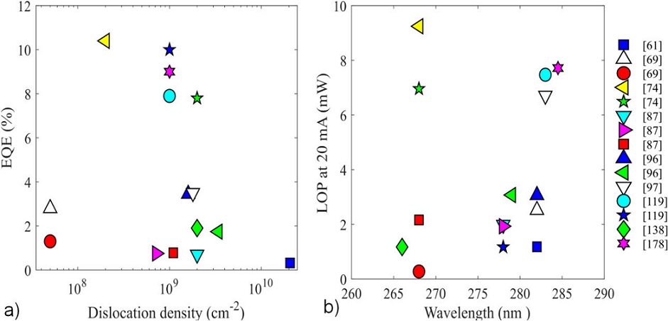
FIGURE 4 Dislocation effect on LED performance a) Relationship between dislocation density and EQE at 20 mA and b) LOP as a function of wavelength.
Furthermore, superlattice structures (SL) on sapphire substrates are employed in order to decrease the dislocations and prevent cracks as the thickness increases by reducing the tensile strain [99]; these SLs filter the dislocations significantly [73, 100]. Besides, the use of AlN/GaN SLs has shown intense luminescence in the deep ultraviolet region from 4.4 to 5.0 eV (related to the GaN layer thickness) when an AlN/GaN SL (1.8 nm, 0.6 nm, and 0.75 nm) is grown by MBE on a 4H-SiC substrate [101]. Moreover, an AlGaNbased transition layer might be grown after the AlN buffer layer which results in a crack-free smooth epitaxial film with threading dislocations around 3.8×109 cm−2 on a Si sub-strate achieving a roughness of 1.5 nm which is critical to obtain highly efficient quantum wells (QWs) [102].
The challenge of enhancing the active region
Once the substrate has been chosen and buffered, the next step is to study the photoluminescence emission peak, which is directly related to the active region. Here, it is necessary to mention that light emission characteristics can strongly be modified by using different quantum heterostructures such as quantum dots (QD) [103-105], nanowires, and quantum wells (QW) confined between quantum barriers (QB).
Moreover, the efficiency in the active region is closely related to three different types of recombination mechanisms, as shown in Eq. (3), employing the ABC model [106].
where R is the recombination rate, n the carrier concentration, and f(n) the leakage current as a function of the carrier concentration. A, B, and C represent the Shockley-Read-Hall (SRH), radiative, and Auger recombination coefficients, respectively. These three coefficients refer to the recombination mechanisms illustrated in Fig. 5. First, radiative (or band-toband) recombination is the base of photoemission in the active region and involves electrons from the conduction band, which recombine with holes in the valence band, releasing energy as photons during the process. Secondly, SRH recombination plays an important role when high levels of dislocations are present in the structure, generating heat [106]. Finally, Auger recombination is related to the carrier concentration and allows that a third carrier absorbs the energy released by electron-hole recombination, raising it higher in the conduction band or pushing down a hole deeper in the valence band [107].
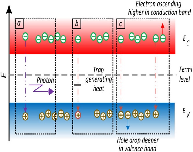
FIGURE 5 Recombination mechanisms, a) radiative recombination, b) Shockley-Read-Hall recombination and c) Auger recombination.
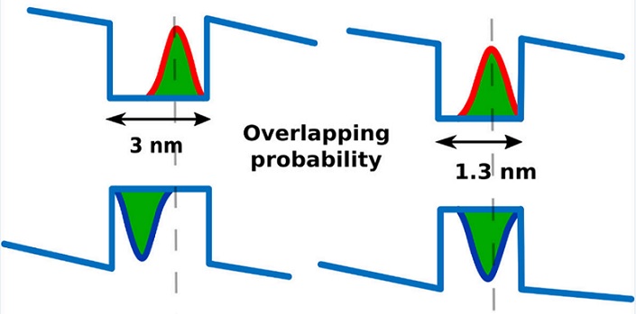
For the optimization of device performance i.e., radiative recombination, the selection of the thickness of the QWs and barriers is crucial. In the hexagonal phase, due to the presence of the spontaneous and piezoelectric fields, the electrons and holes inside the QWs are separated, leading to a decrease in the probability of radiative recombination, as illustrated in Fig. 6a), as well as a shift of the emission toward lower energies. This is known as the quantum-confined Stark effect (QCS) and its influence is shown in Fig. 7a), where the emission wavelength is plotted as a function of QW width (red color line) and compared with the emission without internal electric fields (blue color line) for A l0.61 Ga 0.49 N QWs sandwiched between AlN QBs. For reference, the theoretical data are also compared with experimental results from Haughn et al. [108]. As observed in Fig. 7a), the red-shift of the emission wavelength increases with both the QW thickness and strength of the built-in electric field. Here, it is important to remark that the internal electric field strength is on the order of MV/cm−1 and rises with the Al content and thickness in the barriers, as presented by the theoretical curves in Fig. 7b) and its inset. In this case, the calculation of the electric field includes both spontaneous and piezoelectric polarization and is consistent with previous similar studies [109-111]. These theoretical results show that the QCS effect has a large influence on the QW transition energies, reducing the IQE.
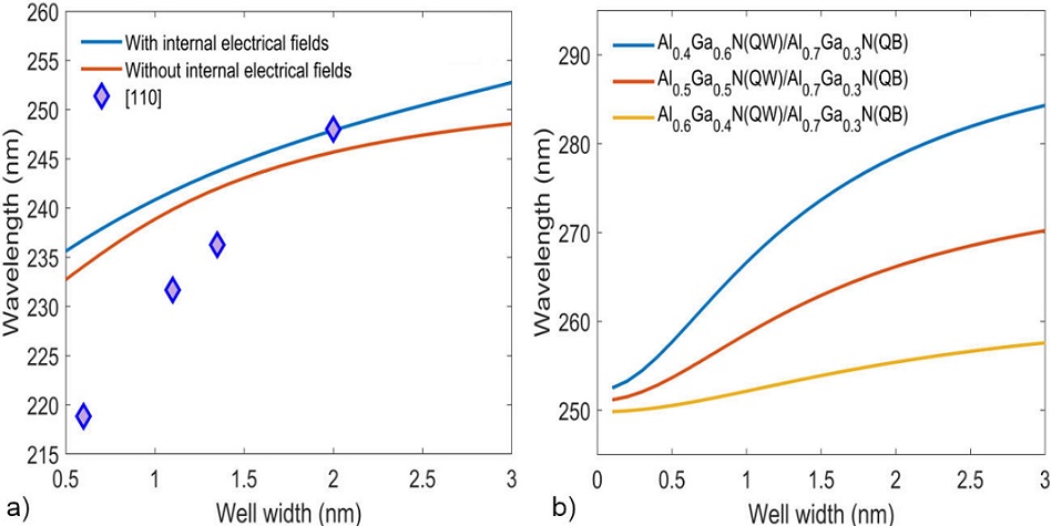
FIGURE 6 QW width effect on emission wavelength of AlGaN-based UVC using QW/QB structure based on a) Al 0.61 Ga 0.49 N/AlN in hexagonal phase, and b) built-in electric field as function of Al mole fraction and thickness (insert) in the barrier. The emission wavelength was calculated using the ground levels in the QWs by solving Schrödinger’s equation. The energy shifts were obtained as described by Phys. Rev. B, 28 (1983) 3241. The built-in electric fields were calculated according to Morkoç, “Handbook of Nitride Semiconductors and Devices”, vol. 1. Wiley-VCH, 2009.
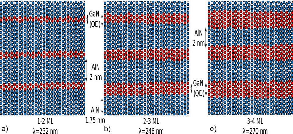
FIGURE 7 QD scheme from Islam et al119 with emission at a) 232 nm (1-2 ML QDs), b) 246 nm (2-3 ML QDs) and c) 270 nm (3-4 ML QDs).
Thus, in order to improve the radiative efficiency in hexagonal AlGaN-based UVC LED, very thin QWs have to be employed so that the QCS effect is mitigated (Fig. 6b)), and the oscillator strength of radiative transitions are increased [80, 112, 113]. For example, Hirayama et al. have investigated the effect of QW thickness on the LOP [114]. They proposed a device structure with 1.3 nm thick QW with remarkable improvement in radiative performance. Therefore, combinations of three aforementioned parameters, i.e., well width, barrier thickness, and Al content, could be engineered to minimize the influence of the QCS effect in opto-electronic devices. For example, aiming for short-wavelength emission, thin wells with a high Al content are required, which increases the built-in electric field as stated above. To compensate, thin barriers could be used to mitigate such an increase.
On the other hand, the QCS effect is not present along the (100) direction of cubic-AlGaN. However, the emission wavelength in this phase is limited by the Al content in the barrier since Al x Ga 1−x N becomes an indirect band-gap material at x = 0.7. Even so, it is possible to use cubic AlGaN material for UVC LEDs. For example, 260 nm emission can be obtained employing cubic Al 0.7 Ga 0.3 N barriers and Al 0.5 Ga 0.7 N wells with a thickness of 1.3 nm. The variation of wavelength with well width is plotted in Fig. 8 for different Al content in cubic QWs. Additional advantages of employing the cubic phase are the easier p-type doping, higher mobility, and perpendicular < 011 > cleavage directions [115]. To further enhance the efficiency, the QB must be designed in such a way that SRH recombination, tunneling leakage, and carrier overflow are mitigated [116].
On the other side, QDs are used to set the bandgap between desired values, with promising results from 232 nm to 270 nm [117]. This change in emission wavelength is made by controlling the thickness of GaN QD (Fig. 9) while keeping them between 1 and 4 monolayers (ML) for the GaN/AlN active region emitting at 225 nm.
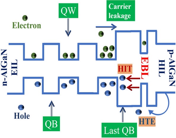
FIGURE 9 Schematic band diagram of MQW-based LED (without internal electric fields effect for simplicity).
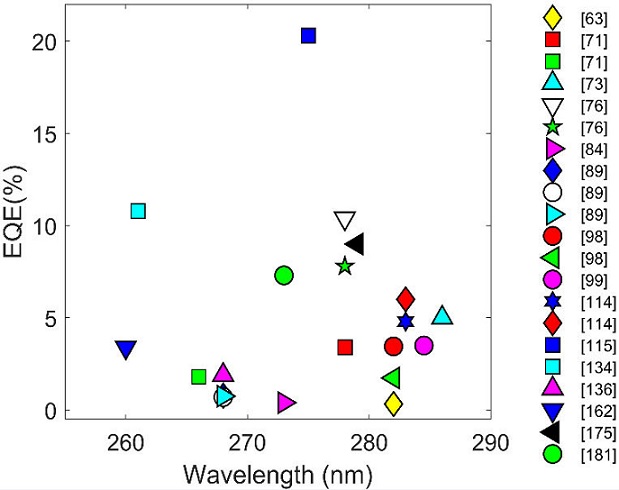
Even though hexagonal-phase LED development has advanced in the UVC range, it is possible to observe in Fig. 10 that some researchers still present EQE equal to 1% and 2% in wavelengths around 220 nm [118] and 280 nm [95], respectively. In order to increase these values, optimization of deposition techniques, materials, and the entire LED fabrication process has allowed witnessing increasingly constant reports with EQE around 10% [74, 119] and up to 20% after a full improvement with an emission peak centered at 275 nm [120]. It has been reported that when both LEE and IQE increase to 60%, it was also necessary the addition a 50 nmAl0.65 Ga0.35N transparent contact layer doped with Mg (hole centration of 8×1019 cm−3), a reflective Rhodium (Rh) electrode, a sapphire substrate, and encapsulation with resin. This IQE increment is due to the transparency enhancement of aluminum nitride templates [121]. Moreover, it has been reported that the use of uneven AlGaN QW with Al content over the 60% allow that IQE increases and, subsequently, the EQE [122].
QW and QB roles in UV emission
In III-Nitrides semiconductors, the asymmetrical behavior of electrons and holes, such as the difference in their effective mass and mobility, deteriorates the performance of devices [123]. Because of that, the concentration of carriers is not uniformly distributed inside of the QW region. Consequently, the radiative performance of the device is degraded especially at high current densities [124]. A number of the strategies are presented for the improvement of performance. In design, researchers are mainly focused on hole injection into the active region because of its high effective mass. Usually, in the conventional structure of UV-LEDs, a single layer for the electron blocking (EBL) is used, i.e., p-AlGaN, for better confinement of carriers inside of the active region.
The EBL provides a high barrier in the path of high-energy electrons, in this way, leakage of electrons from the active region is reduced. Besides, EBL affects the hole injection efficiency into the active region due to barrier height. In this situation, most of the holes are injected by thermionic emission. The phenomena of hole injection by thermionic emission can be improved by interplaying two factors: hole concentration and valence band offset [125]. Moreover, the difference in the content of Al composition in the last QB and EBL leads to the formation of a polarization field. Various approaches have been reported in which holes are injected by both thermionic emission and intra-band tunneling. Khan et al. have reported the feasible solution for the reduction in Mg-diffusion from p-doped EBL to the active region and hole injection by intra-band tunneling [125]. They have reduced the thickness of the final QB (Al content same as in EBL) and introduced a valley in EBL with low Al content in comparison to EBL layers, simultaneously in the proposed device structure. For a better understanding, the schematic band diagram of the device structure is shown in Fig. 11. Consequently, the proposed structural strategy of the device is supported for the enhancement of intra-band tunneling (HIT) and hole by thermionic emission (HTE) because of the decrease in valence band offset, meanwhile the issue of uneven distribution of carriers inside the active region is also reduced.
Regarding the thickness of QWs and QB, several researchers have reported that thicker QW and QB leads to the uneven distribution of carriers inside the active region which degrades the radiative performance [126,127]. Due to thicker QB, the hole tunneling inside of the active region is reduced. Khan et al. have studied in detail the effect of the last QB thickness by introducing the last QB with different thicknesses (4, 6, 8, and 10 nm). They concluded that the device structure with a thickness of 6 nm exhibited the best performance among all of them. Since for 4 nm QB, the chance of Mg-diffusion towards the active region is also increased. Therefore, for the compensation of both, hole tunneling and Mg-diffusion, the thickness of 6 nm QB is reported to be the best.
EBL and p-type layers
Despite the increase in the IQE by reducing the dislocations, enhancing the active region and contact layers, electron leakage due to high operating currents and the associated heating affect the LED, causing an efficiency droop, decreasing the EQE to values lower than 5% [128]. While p-type AlGaN layers with high Al content used as hole injection layer (which commonly goes under p-type contact layer shown in Fig. 3) have low hole concentration (lower than 1 × 1017 cm−3) and will provoke parasitic emissions [129]. Enhancing the radiative recombination by increasing the carrier confinement in UVC LED also requires leakage electron blocking.
For performing the EBL, it is necessary high Al content to avoid that the electrons absorb energy without emitting the expected UVC radiation. However, high Al content drawbacks in design. To solve this, some approaches have been studied such as p-type electron blocking layer (p-EBL), pEBL superlattices, and graded superlattices [128-132]. By applying an EBL with an SL structure, the effective barrier height at the valence band is decreased. On the other hand, the conduction band is increased, mitigating the electron leakage while the hole injection augments [75]. It has been demonstrated that the inclusion of p-EBL superlattices to the LED structure allows achieving high EQE compared to similar LEDs without EBL 131 and even increasing around 90% more EQE by reducing the efficiency droop to 4% in LEDs emitting around 270 nm [128].
Another approach to improve LED performance is to substitute the conventional EBL with graded EBL, step graded and step graded superlattices, which have presented IQE up to 37.4% and 15% less efficiency droop with an emission peak at 224.76 nm [78]. Besides, the implementation of a layer that allows blocking the holes just like the EBL blocks the leaking electrons have been recently investigated. This Hole Blocking Layer (HBL) implementation has been demonstrated to enhance both the light-output power (24.2 mW to 56.1 mW) and IQE (from 32% up to 72%) [76]. In other words, by growing HBL between the active region and n-type layer, the radiative recombination augments, and the hole leakage is prevented [76,77].
As mentioned above, EQE is an essential parameter to measure the efficiency of LED devices. Thus, different approaches to enhance this value are explored above. Another critical path is to replace the typically used p-GaN with pAlGaN as a contact layer to reduce the UV absorption. However, this is a complicated task because of the high activation energy necessary to implant Mg 120 from 160 meV [133] to 500 meV [134], even up to 630 meV [135]. Despite this, it has been demonstrated that improving the transparency of contact layers enables the LED to increase EQE at least 5% by changing Ni/Au electrodes for Ni/Al electrodes [71, 136]. Also, EQE can be improved 3% more through rising hole concentration in p-AlGaN, despite the drawbacks that p-doping AlGaN:Mg involve, finally superseding GaN contact layer [71].
Until this point, the mechanism for enhancing efficiency in UVC LEDs have been discussed, considering the results depending on what previous works reported. However, several considerations must be done such as p-doping drawbacks when high Al content is used in AlGaN alloys, how this high Al content benefits the material transparency and what is needed to decrease the specific resistance of materials and allow a more efficient carrier injection to the active region [117,137,138].
Whereas p-GaN ohmic contact growth is studied to improve the efficiency [139], the use of AlGaN in the p-type doping and growth of ohmic contacts remains in search to become more functional. Although 7% more EQE at 276 nm emission peak has been reported by the implementation of a p-AlGaN transparent contact layer is implemented, when the wavelength is shortened to around 260 nm, the EQE droops to 2.3%-3.3% [136, 138]. For the p-contact layer increases the transparency, it is necessary to substitute the typical GaN contact layer with AlGaN with high Al content; however, the more Al content is in the alloy, the greater activation energy for p-type doping is needed [140].
P-type doping and ohmic contacts
Since growth and doping required both accuracy and fine control of fluxes, epitaxy is used as the main deposition technique for LED fabrication. In this way, there are three epitaxial techniques more used such as molecular beam epitaxy (MBE), migration enhanced epitaxy (MEE), and metalorganic chemical vapor deposition (MOCVD) [141-144]. Besides, the development of combined methods based on MBE, MEE, and MOCVD, such as metal-source flow-rate modulation epitaxy, are of interest as long as Nitrogen flux remains constant reducing the activation energy of acceptors and smooth surfaces could be produced [145]. On the other hand, besides the deposition technique used for growing, in order to obtain high p-type doping levels, it is necessary to consider that while cubic phase p-GaN has demonstrated recently to reach an Mg concentration of 1020 cm−3 for III-V semiconductors, it must be considered that this value is approaching the solubility solution limit which could cause a strong drop in hole concentration because of selfcompensation that involves Mg−V N complexes [146]. However, it is remarkable to note that hole concentration over 1019 cm−3 with a mobility of 3 cm2/Vs point to c-GaN is a suitable alternative to obtain high free hole concentration for cubic-structures-based LEDs [146]. In addition, considering the current state of art emphasizes the use of hexagonal phase for UVC LED development, the doping of AlGaN is more complicated than GaN doping (p-type more restricted than n-type), because of the high activation energy of Mg around 630 meV (for AlN:Mg) [135, 143], and the maximum solubility of dopants in III-nitrides semiconductors [105]. Thus, bulk structures, superlattices, grading the Al content, even δ doping techniques have been studied to increase the hole concentration without affecting other properties [134,147,148], and SL has been demonstrated to diminish the activation energy for doping improvement [149].
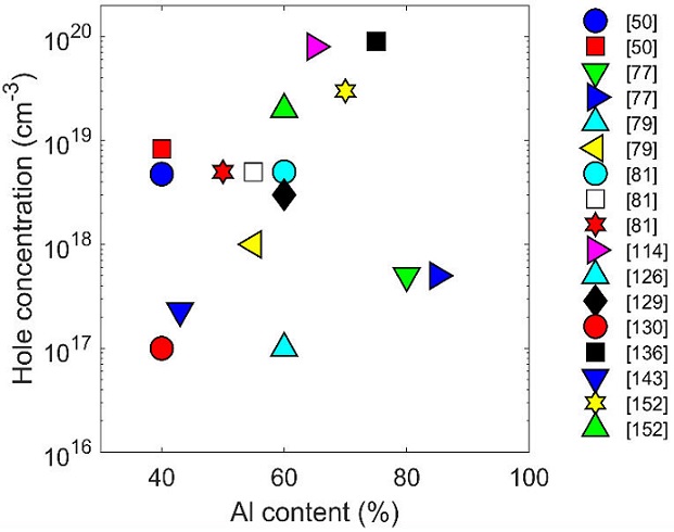
Although the drawbacks above, Fig. 12 suggest that the free hole concentration range of 1017 −1019 cm−3 is a reasonable interval to consider when it comes to the hole concentration for Al content between 50% to 80%. Besides, it is important to mention that the material resistivity and transparency of AlGaN layers are augmented as long as Al content increases since the Al is added to the GaN the electronic mobility is diminished which results in a resistivity increase despite a high hole concentration (over 1019 cm−3) [150].
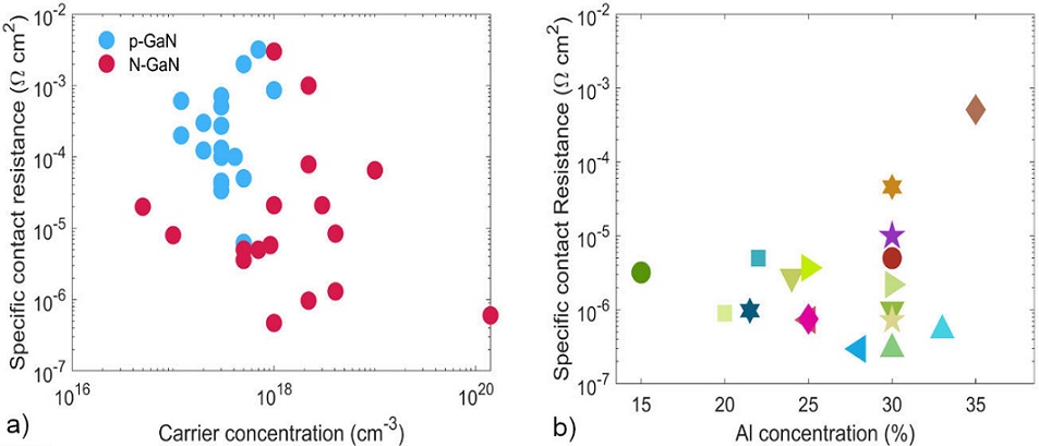
FIGURE 12 Specific contact resistance performance based on Greco et al[161], a) Differences between p-GaN against n-GaN heterostructure as the contact layer b) Al concentration vs Specific contact resistance in AlGaN/GaN heterostructures.
All growth and doping improvements have allowed that bulk structures are not the only option for UVC LED elaboration. For example, the accuracy provided by epitaxy makes it possible to create nanostructures and thin superlattices to set the energy band between the UVC range. The use of Al x Ga 1−x N/Al y Ga 1−y N superlattices makes the resistivity less independent on temperature, increasing the free hole concentration even under low temperatures, reaching up a hole concentration of about 3.5×1018 cm−3 without sacrificing resistivity based on Al 0.63 Ga 0.37 N/Al 0.51 Ga 0.49 N superlattice structures [151]. Moreover, other works suggest the use of a quaternary alloy of AlInGaN to replace the p-AlGaN intermediate layer (between the active region and ohmic contact) to reduce the IQE droop by enhancing the hole injection to the active region [152].
A different approach, to upgrade the p-type doping results, is to gradually add Al to GaN and carry out the doping process to increase the LOP and reduce the forward bias polarization. At the same time, the disadvantages of the electron blocking layer are avoided [153, 154]. When the Al content in a p-contact layer is graded, both the electron and hole concentration increase in the active region mainly due to the low effective potential height for holes which improves the hole injection to the active region [155]. Besides, the non-radiative recombination associated with holes and leaked electrons is reduced by the high effective electron barrier height, demonstrating the advantage of the graded active region over bulk layers [155,156]. Another structure with more efficient performance is the superlattice. In this structure the hole mobility is increased by a factor of five compared to a bulk structure, reducing the resistivity using polarization effects [157,158].
As mentioned above, one more doping strategy is based on dopant distribution which is described by Dirac’s δ function, the δ-doping [159]. This has proven to be an effective method to improve the conduction of AlGaN p-type layers with high Al content by the self-compensation reduction whereas hole concentration increases 50. This enhancement is due to the use of In as a surfactant, which allows that incorporation of Mg increases, diminishing the activation energy of the acceptors whereas p-type conductivity augments [50]. Furthermore, it is remarkable to mention that, in n-type, δ-doping has presented results even more promising than graded or superlattices [160].
Ohmic contacts are the interface between electronic circuitry and the light-emitting device. Thus, the contact resistance is closely related to power losses of the entire system [161]. To achieve an efficient UVC LED, this should have low resistances in its contact layers. The n-type contact gives a massive component of resistance to the device when high Al content is used, thus, by using Si as n-AlGaN dopant the specific resistance of the material is reduced whereas the electron concentrations tends to 1019 cm−3 [162] The stateof-the-art presents free electron concentrations around 1018 cm−3 under 60% of Al, this value, parallelly have reported contact resistance over 10−6 Ωcm2 by using V/Al/Ni/Au electrodes [163]. Nevertheless, while Si doping levels rise, n-AlGaN layers start to behave as an insulator due to the selfcompensation [164].
As Fig. 13a) shows, the p-type ohmic contact deposition is more complicated than the n-type because of the pdoping drawbacks mentioned in the previous section. Commonly, p-GaN is used for UV LED despite its opacity resulting in low extraction of the light. However, it is also reported that p-AlGaN contact layers have been shown to increase LEE [165, 166]. Moreover, superlattices based on Al x Ga 1−x N/Al y Ga 1−y N or Al x Ga 1−x N/GaN are used instead of the typical GaN p-type contact layer due to the tunability of the energy gap by changing the Al content and the lower resistance [167-170]. The specific contact resistance varies between 10−4 Ωcm2 and 10−7 Ωcm2, depending on the Al content in AlGaN/GaN, as shown in Fig. 13b) even without doping the AlGaN/GaN heterostructure and considering the low concentration of Al, the specific contact resistance remains lower than p-GaN ones. Despite AlGaN/GaN heterostructures contact resistance is lower than GaN resistance as shown in Fig. 13a), it is useful to growth a thin p-GaN layer to guarantee Ohmic contact deposition without depending on negative effects caused by the addition of Al [166], a thin p-GaN layer (< 10 nm) over the superlattice has also been used as a low resistive ohmic contact [171]. On the other side, to improve the EQE despite a low hole concentration in p-Al0.6Ga0.4N doped with Mg, the use of High Reflective Photonic Crystals (HR-PhC), over the p-contact layer have been proposed to facilitate the tunneling effect which enhances the LEE [70] even though hole concentration drops down to 103 cm−3 [119].
Once the contact layer has been grown and the n-contact layer is exposed by wet or dry etching techniques [172-174], ohmic contacts that provide the correct electron injection to the active region must be deposited. The most used metals are Nickel/Gold (Ni/Au) [139,163,170,175], this is because the Ni work function is greater than the p-contact layer work function, avoiding that a Schottky barrier is generated on the p-type material [176,177] and also it has been reported that as the Ni thickness decreases to around 0.8 nm, the reflectivity augments [178]. However, elements such as Vanadium, Platinum, and Rhodium (V, Pt, Rh), are used to diminish the specific contact layer [163,164,179,180], by substituting Au with Silver (Ag) the specific contact layer is comparable with those that use Au [171], even more useful due to the increase of reflectivity reaching contact resistance up to 3.5 × 10⁻⁵ Ωcm2 [181].
Conclusions
In summary, to increase UVC-LEDs’ efficiency for germicidal applications, several considerations must be performed. First, it is essential to deposit a buffer layer that absorbs strains to reduce the propagation of structural defects to the next layers [102]. Most of the works reported in the stateof-the-art point out the hexagonal crystal structure for UVC devices mainly due to the cubic phase direct-indirect bandgap cross point around 70% of Al in AlGaN alloys 56. However, the development of c-AlGaN-based UVC LED is feasible if the quantum confinement is increased despite the reduced Al content available before exceeding this cross point by employing thin nanostructures such as 1.3 nm-thick QW with Al content around 50% and 70% for QW and QB, respectively, in the active region emitting at 260 nm, as suggested by Figure 8. It must be considered that while the wavelength increases from 260 nm, greater doses are needed to reduce the virus load 26. Furthermore, the Al x Ga 1−x N p-type doping is limited by the Al molar fraction (x) due to the activation energy increases as the Al content increases reaching to ∼ 630 meV for h-AlN (x = 1) [135, 143]; nevertheless, different approaches to diminish the high Al content effects are implemented [151-153, 155, 156] allowing to conclude that the superlattices structures [151,152,182] and Al content graded p-regions [153,155] are the most promising approaches for the p-type doping by decreasing activation energy [149]. The typical p-GaN contact layer must be substituted with a more transparent highly doped p-AlGaN hole transport layer to ensure low contact resistance by selecting the appropriate electrodes [164-171]. It is remarkable mentioning that the UVC-LED EQE record is 20.3% emitting a UVC radiation centered on 275 nm, by employing a sapphire patterned substrate to reduce threading dislocations, substituting p-GaN for p-AlGaN to reduce the absorption in the contact layer, the use of Rh mirror electrode and HR-PhC to increase reflectivity and resin coating. However, we suggested in addition to previously discussed efforts for an EQE of 20%, the use of superlattices in the EBL and p-cladding layer could improve the EQE due to a reduced hole leakage and increased hole injection, respectively. Moreover, the advantages of the cubic phase over the most studied hexagonal one, such as low Mg activation energy due to crystal symmetry [146], the absence of spontaneous and piezoelectric fields in the active region (as discussed in Fig. 7), and the possibility to emit UVC-radiation supported by our QW calculations without exceeding direct-to-indirect band gap cross point limit with an expected emission at 260 nm are strong arguments to consider the c-AlGaN UVC-LED as an emergent candidate to overcome the current EQE.
Declaration of interests
The authors declare that they have no known competing financial interests or personal relationships that could have appeared to influence the work reported in this paper.

