


 nova página do texto(beta)
 Inglês (pdf)
 Artigo em XML
 Referências do artigo
 Enviar este artigo por email
 Citado por SciELO
  Similares em
SciELO
Similares em
SciELO 
 Permalink
1. Introduction
Surface plasmons (SP) are collective oscillations of charge located between the surface of a dielectric and a metal [1], which have made it possible to improve and reduce the dimensions of electronic devices [2-4]. In biomedicine, they are being used in photothermal therapies and cancer treatments [5,6], as well as their use to convert solar energy into chemical energy [7]. Recent studies have shown that systems formed by plasmonic nanostructures can be used as nano heat sources [8,9].
Among the traditionally used metals in plasmonics, silver (Ag) and gold (Au) stand out, because they have a wide range of the electromagnetic spectrum in which SP can be excited, ranging from infrared (IR) to visible (Vis) with energy losses at ∼ 318 nm and ∼ 517 nm as a result of their interband transitions (IT) [10,11] respectively.
On the other hand, aluminum (Al) is a metal that has begun to be explored for plasmonic applications [12,13], which in comparison with Ag and Au, has some advantages, such as a broader SP excitation range that goes from ultraviolet (UV) to IR; it has a layer of native self-limited oxide ∼ 3 − 4 nm [14] that protects it from corrosive environments, as well as being cheaper. Due to its high density energy, it can release large amounts of energy through the SP-assisted combustion process (a phenomenon known as photo-ignition), which can be applied for the development of nanosolders, nano propulsures or nanoexplosives [15].
Zheng et al. [16] have shown that hot carriers (hot electrons) induced by plasmons, can be used in two-dimensional structures to generate photocurrents [17], with the capacity to transfer their energy to phonons [5], producing temperature increases in nanometric areas in a matter of femtosecondsm[18].
It has recently been shown that it is possible to excite SP at certain wavelengths by varying the metal nanostructures dimensions of Al, Pb, and Ag [19-21]. In this work, Al thin films have been deposited on nanostructured substrates called aluminum metafilms (Al-MF), obtained by electrochemical anodization. By varying the dimensions of the Al-MF, it was possible to excite SP at determined wavelengths in the range ∼ 420 − 770 nm. Increases in temperature (T) and changes in electrical resistivity (ρ) of Al-MF were recorded when irradiated with different wavelengths.
2. Experimental details
For the synthesis of the nanostructured substrates, Al foils (Sigma Aldrich, 0.25 mm thick, 99.999% purity) were used, which were annealed in an H2 atmosphere at 600◦C for 6 hrs. Subsequently, they were electropolished in an electrochemical cell using as electrolyte a solution of perchloric acid and ethanol in a ratio of 5:1 vol., applying voltages of 18 V for 2 min maintaining a temperature of ∼ 3◦C, in this way, it is possible to obtain a homogeneous surface like the one shown in Fig. 1b).
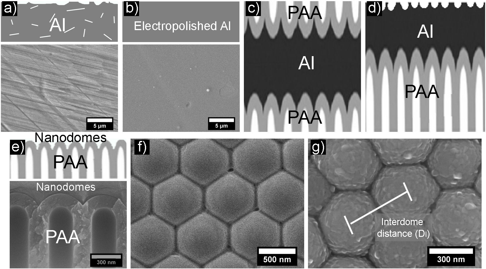
FIGURE 1 Schematic representation and SEM micrographs of the Al-MF synthesis process. a) Al foil without treatment. b) Electropolished Al foil. c) PAA obtained after the anodization process. d) Elimination of the PAA. e) Cross-section and f) Top view of the nanostructured substrates (nanodomes). g) Al film deposited on a nanostructured substrate (Al-MF).
In the anodization process graphite was used as the cathode and Al as the anode. The anodizing voltages were in the range of 130-250 V supplied by an adjustable DC power source (BK PRECISION model 9185B). The electrolytes used were chosen depending on the applied anodizing voltage [19].
From the anodization process, a type of Al oxide known as Porous Anodic Alumina (PAA) was obtained (see Fig. 1c)). Subsequently, using a solution of NaOH (2.5M) and HCl (20% weight), the PAA was eliminated from one of the faces of the foil; afterward, the residual Al was removed with a solution of CuCl2 (0.5M) (Fig. 1d)). With this process, the nanostructured substrate (nanodomes), shown in Figs. 1e) and 1f), is obtained.
On the nanodomes (Fig. 1f)) a thin film of Al of ∼ 50 nm thick was deposited by thermal evaporation using pressures of ∼ 5 × 10⁻⁶ torr, thus obtaining what we denominated Al-MF (Fig. 1g)). Its morphology was evaluated using a field emission scanning electron microscope (SEM) JEOL 7600F equipped with an energy dispersive x-ray spectrometer (EDS). The geometric parameters of the Al-MF, such as the interdome distance (D I ) (Fig. 1g)) were obtained using the Image J software [22]. After, employing a UV-Vis spectrophotometer (UV-2600 Shimadzu Corporation), the specular reflectance measurements were performed at an angle of incidence of 8◦in a range of 190-1400 nm.
The measurements of T as a function of the intensity of incident radiation were carried out at a pressure of ∼ 5×10⁻³ torr, using a K-type thermocouple of ∼ 0.2 mm diameter attached to the sample using silver paint (Colloidal silver paste-EMS). The samples were irradiated in an area of ∼ 0.8 mm2 using monochromatic CW laser light sources of 445, 532 and 650 nm, varying the incident intensity in an interval of 0 − 4 × 10¹⁸ photons/(s)cm2 (Maximum power of the lasers). Finally, measurements of ρ as a function of T were carried out in the range of ∼ 100-370 K, using the four-terminal sensing, in darkness and under an intensity of 1 × 10¹⁶ photons/(s)cm2 using the three wavelengths. For these measurements, the maximum light intensity was chosen monitoring the electrical resistance in situ while increasing the intensity and was stopped when we detected a minimum change; with this procedure we think the overheating is minimized.
3. Results and discussion
In Fig. 2a), an SEM micrograph of an Al film deposited on a non-texturized substrate (glass) is shown, while in Figs. 2b) and 2c) Al films deposited on texturized substrates (nanodomes) are shown. In these last two cases, it can be seen that the Al film follows the morphology of the substrate.

FIGURE 2 SEM images of 50 nm thick Al films on a) Non-texturized substrate (glass), b) and c) Texturized substrates with different anodizing voltages.
The values of the interdome distance (D I ) obtained from the SEM images (Fig. 1g)) were in the range of 415.5±57.8− 786.9 ± 90.3 nm. The D I value depends on the applied anodizing voltage [19-21].
In Fig. 3a) the reflectance spectra as a function of the wavelength of Al-MF with different D I values are shown. In all cases, minima are observed in the ∼ 420−770 nm wavelength range attributed to first-order surface plasmon resonances (SPR) [1]. The position of these minima can be calculated using as a first approximation the electromagnetic wave coupling model and SPR in two-dimensional periodic arrays with hexagonal geometry, given by [24]:
where ε m and ε d are the dielectric functions of the metal and the dielectric (in our case air, ε d = 1), respectively; θ is the angle of incidence of the electromagnetic waves, D I is the period of the array (in our case the interdome distance) and i,j the orders of dispersion. In Fig. 3b), experimental data corresponding to the dip position observed in the reflectance spectra of Al-MF as well as its respective theoretical curve obtained from Eq. (1) [20] are shown.

FIGURE 3 a) Reflectance spectra of Al-MF with different D I . The results for the non-texturized Al film (gray curve) are shown for comparison. b) Experimental data obtained from Al-MF. The analytical curve of SPR (red curve) was performed using the model given by Eq. (1) with an incidence of 8◦and the optical constants for Al reported in [23].
As shown in Fig. 3a), the position of the minima corresponding to SPR (λ SPR) in the reflectance spectra depends on the dimensions of the D I . In addition, another dip is observed in all samples at 826 nm related to IT in Al [25,26]. It is worth mentioning that the theoretical model given by Fig. (1) reasonably follows the experimental results (Fig. 3b)). This behavior has also been observed in Ag and Pb metafilms [20]; which demonstrates the possibility of the excitation of surface plasmons in different texturized metals.
For measurements of T as a function of the intensity of incident radiation, Al-MF were synthesized with λ SPR = 445 nm and λ SPR = 532 nm. According to the results shown in Fig. 4, the increases in T are in the range of 16 − 204 K considering the ambient T(∼ 294 K). For the case of the non-texturized Al film (Fig. 4 a) ), the maximum reached temperature was ∼ 316 K using an incident three wavelength of 650 nm (λ inc = 650 nm); while for Al-MF with λ SPR = 445 nm and λ SPR = 532 nm (Figs. 4-b) and 4-c)), the reached temperatures were ∼ 432 K and ∼ 498 K, respectively. In these last two cases, the increase in T by radiation was greater compared to the non-texturized Al film. In particular, overheating occurs when Al-MF is illuminated with a wavelength close to or equal to its SPR, that is, when λ inc ≈ λ SPR. Under these conditions, the SP decays in a non-radiative way, generating hot electrons [16] that transfer their energy to the phonons, thus increasing T locally [5].

FIGURE 4 T curves as a function of the intensity of incident radiation in a) Non-texturized Al film. Al-MF with b) λ SPR = 445 nm and c) λ SPR = 532 nm. The intensity of light begins increasing from zero (Light on) up to a maximum intensity of 4×10¹⁸ photons/(s)cm2 (Maximum power), then it is decreased again to zero (Light off); the total process made in a time of 1 minute, such as is observed in the horizontal axis. The color of the curves corresponds to the shown wavelengths.
Measurements of ρ as a function of radiation exposure time (t exp) were performed using an λ inc = λ SPR = 445 nm with power of 4 × 10¹⁸ photons/(s)cm2. As shown in Fig. 5 a) , when t exp is ∼ 1 s there is an increase in ρ from ∼ 1.3 × 10⁻⁶ Ωcm to 2.3 × 10⁻² Ωcm. In this case, the Al-MF does not show notable deterioration; in addition, its ρ returns approximately to the initial value (∼ 1.5×10⁻⁶ Ωcm) before being exposed to radiation. On the other hand, in Fig. 5b) it is observed that if the t exp is greater than 1 s, the value of ρ continues to increase due to local overheating in the sample. In particular, at t exp = 4 s, a change in the slope of ρ is observed due to the degradation and subsequent evaporation of Al-MF (see inset Fig. 5b)); in this case, ρ does not return to its initial value when irradiation is ceased.

FIGURE 5 Al-MF ρ curves with λ SPR = 445 nm irradiated with an intensity of ∼ 4 × 10¹⁸ photons/(s)cm2 and a) t exp = 1 s and b) t exp > 4 s; the inset image belongs to the photograph of a sample damaged by local overheating.The samples were progressively irradiated (Light on) to the laser’s maximum power and back to darkness (Light off) c) SEM images from the morphology evolution of an Al-MF irradiated at the different t exp shown in the text.
Figure 5c) shows SEM images of the evolution of the morphology of an Al-MF with λ SPR = 445 nm when irradiated with an λ inc = 445 nm at a power of 4 × 10¹⁸ photons/(s)cm2 to a different t exp. The change in its appearance (degradation) due to local overheating is clearly observed.
Locally, the temperatures reached by overheating due to non-radiative decay of SP are estimated to be ∼ 933 K (melting point of Al), although it has been reported that the melting point of Al may decrease as the size of the particle decreases (∼ 3 K for a particle radius of ∼ 40 nm) [27], in our case we estimate that the effect must be negligible since the thickness of our film is 50 nm and continuous. Recently, it has been shown that by the excitation of SP in Al nanoparticles, it is possible to achieve a T of ∼ 975 K [15].
To qualitatively show the increase in T in located areas, a drop of water of 1 cm in diameter was placed on an Al-MF with λ SPR = 445 nm and it was irradiated with an λ inc = 445 nm with 1 mm diameter at normal incidence, at a power of ∼ 4 × 10¹⁸ photons/(s)cm2. Figure 6 shows the experimental setup, where water vapor bubbles are observed in the area where the laser hits. These appear because temperatures above the boiling point of water are reached (see Fig. 4b)). This fact could be applied to water purification methods [28], to the development of plasmon-mediated nano heat sources[8], cancer treatments [5], or to generate and control microbubbles, since they are highly relevant in fundamental problems in thermodynamics in the study of local heating of fluids [9]. The following reference shows a video of the observed phenomenon [29]. When the water vapor bubbles are generated, a sound can be perceived, which we assign to a possible phenomenon of nanocavitation [9].

FIGURE 6 Water vapor bubbles induced by overheating in an AlMF with λ SPR = 445 nm when it is irradiated at normal incidence with a laser light source of λ inc = 445 nm.
On the other hand, according to Figs. 5a) and 5b), the changes of T in the Al-MF cause a considerable effect on the ρ, it is for this reason that measurements of ρ(T) were carried out irradiating the samples under the same lighting conditions and low intensity 1 × 10¹⁶ photons/(s)cm2. Figure 7 shows the curves of ρ(T) for a non-texturized film (reference sample) (Fig. 7a)) and Al-MF with λ SPR = 445 nm and λ SPR = 532 nm (Figs. 7b) and 7c), respectively).

FIGURE 7 Curves of ρ(T) in the dark and using different three wavelengths. a) Non-texturized film. Al-MF ∼ 50 nm thick with b) λ SPR = 445 nm and c) λ SPR = 532 nm. In all cases, a reference line (pink line) and the Al Debye temperature (T D = 428 K, orange line) [30] were placed. The continuous black curve is before the illumination process, the red, green, and blue curves correspond to the illumination with wavelenghts of 650, 532, and 445 nm, respectively, while the dashed black curve is after the illumination process.
In Fig. 7, it is observed that ρ decreases when T decreases in all cases, which is the typical behavior in metals [30]. But the linear behavior of ρ as a function of T below the Debye temperature ( D) is slightly modified (see the reference pink line). We attribute this behavior to the fact that the electron undergoes scattering due to the texturing present in the samples (Figs. 7b) and 7-c)). It is also observed that in a second measurement in darkness in the Al-MF (dashed curve) ρ is slightly higher than the first one (black curve), possibly due to the deterioration caused by local heating when irradiated, even when the used light intensity is low; this effect is more noticeable at low temperatures.
4. Conclusions
The texturing of Al-MF allows a higher efficiency of absorption of light energy that is transformed into heat compared to non-texturized films. When Al-MF are illuminated with λ inc close to or equal to their λ SPR, localized overheating occurs due to non-radiative deexcitation of surface plasmons and the creation of hot electrons that transfer their energy via phonons and finally heating the Al metafilm. This overheating causes a deterioration of the material and, consequently, a change in the ρ of the Al-MF.

