


 nova página do texto(beta)
 Inglês (pdf)
 Artigo em XML
 Referências do artigo
 Enviar este artigo por email
 Citado por SciELO
  Similares em
SciELO
Similares em
SciELO 
 Permalink
1. Introduction
Continuous technological development has triggered the search for new materials that comply with specific properties for avant-garde devices and new manufacturing techniques. In the microelectronics industry, the Ultra Large-Scale Integration (ULSI) as well as the current generations of CMOS and MOSFET devices, among others, tend to require thin insulating layers of around 30 A. Silicon dioxide (SiO˚ 2) has been used with great success. However, for new devices, silicon dioxide films with thicknesses of ∼ 30 A, present tunneling through the potential barrier and impurities diffusion. As a result, other types of materials have been investigated to replace SiO2 [1].
In recent years, much research has been conducted on HfO2 and related compounds thanks to their excellent physicochemical properties, high refractive index, and bandgap energy of 5.68 eV [2-3]. Its transparency extends over a wide spectral range, from ultraviolet to medium infrared [4-6]. Consequently, this material is widely utilized for optical applications as a protective layer due to its thermal stability and hardness, and it is also used as a gas sensor [7-11]. HfO2 films are susceptible to doping with different rare earths, emitting at different colors depending on the dopant when excited with UV light. Crystallinity allows the incorporation of this type of ions [12]. The most common precursors used to synthesize HfO2 are chlorides and metal-organics. In particular, hafnium acetylacetonate (Hf(acac)4) is used due to its low melting temperature (≈ 200◦C), as well as its ease of dissolution in N, N-Dimethylformamide (N,N-DMF). It is a solvent with a high dissolution capacity with acetylacetonates. This solvent has successfully been used to synthesize other materials, such as aluminum and zirconium oxide [13,14]. Due to its high dielectric constant as an insulator, HfO2 has received considerable attention in the field of microelectronics as an alternative material to silicon oxide in the next-generation MOS devices [15-16].
Many techniques have been applied in the synthesis of hafnium oxide films [17-24]. Ultrasonic spray pyrolysis has proven to be an efficient, versatile, and low cost technique for depositing thin films that can be scaled at an industrial level since it does not require a vacuum equipment operation, making the depositing processes more expensive [25-27].
The present article shows an alternative method of depositing HfO2 thin films by adding deionized water by ultrasonic spray pyrolysis. HfO2 films were also synthesized without water spray during deposition to evaluate the method, keeping the other deposition parameters constant. The characterization was carried out utilizing XRD to determine the crystalline structure formed under various growth conditions. Refractive index and thin film thickness were determined through ellipsometry. AFM shows the HfO2 thin film surface morphology and rugosity values. With SEM, the morphology of the deposits was shown. IR measurements allowed to determine the types of existing ligands and establish water effect on the growth of HfO2 films. Finally, the electrical characterization was done by C-V measurements, from which the dielectric constant for the films was acquired. Our results show that deposit of HfO2 thin films by ultrasonic spray pyrolysis, adding deionized water, can be successfully used, allowing to obtain adequate dielectric values and low roughness values, making HfO2 a right substitute candidate for SiO2 in the fabrication of MOS structures.
2. Experimental procedure
2.1. Experimental setup
Figure 1 presents the experimental setup consisting of a compressed air tank, used as the carrier gas, a regulator at the entrance, and a flow meter. Two ultrasonic generators operate at 780 kHz, the first container restrains the Hafnium (Hf) salt dissolved in N-dimethylformamide (N,N-DMF), and the second one contains deionized water, both connected to a pair of glass nozzles joined to plastic hoses that allow directing the generated aerosol to the surface of the substrate. The separation between nozzle and substrate is 5 mm. The substrates are placed in the molten tin bath. The temperature of the system increases linearly using a controller. A thermocouple allows instant monitoring of the temperature of the tin bath. The system is enclosed in an acrylic chamber connected to a gas extraction system.

2.2. Materials and synthesis of HfO2 thin films
Hafnium oxide, HfO2, films were synthesized by ultrasonic spray pyrolysis. Two types of substrates were employed, ntype Si (111) and Si (100), high and low resistivity, respectively, both for electrical and structural characterization.
Hafnium acetylacetonate (Hf(acac)4, Alfa Aesar, 97%) and N,N-DMF were used as HfO2 precursors at a 0.035 molarity. We followed two synthesis paths. Hf(acac)4 and N,N-DMF were mixed in an ultrasonic nebulizer in the first path. Two ultrasonic nebulizers were applied; the first contains Hf(acac)4 and N,N-DMF, while deionized water (18 MΩcm−1) was added to the other one. Dry air was utilized as carrier gas at 10 liters per minute (lpm) for the Hafnium source and 3 lpm for the aerosol deionized water. The deposit was carried out at four different substrate temperatures: 400, 450, 500, and 550◦C (the deposit time was 5 min in all cases). MOS contacts were made over the films through thermal evaporation of aluminum, achieved in a high vacuum evaporator (10−5−10−6 mbar), using a stainless-steel mask over 0.011 cm2 with circular perforations.
2.3. Characterization of HfO2 thin films
Thicknesses and refractive indexes of the HfO2 films were found in an LSE Stokes Ellipsometer (Gaertner). A MagnaIR 550 FTIR (Nicolet) was employed to obtain the IR spectra in the 400-4000 cm−1 region, and grazing incidence Xray diffraction (GIXRD) was performed on a Siemens D5000 diffractometer for structural characterization. The rugosity was determined utilizing an Atomic Force Microscope (AFM) from Thermo Microscopes Veeco model auto probe CP with 10 µm scanner, and a Sirion LX30 Scan Electron Microscope (FEI) was employed to determine the morphology. A JSM-6300 (Jeol) with an EDS detector (NORAN 660B1555) was used to get chemical composition. The C-V electrical analysis was carried out with a Keithley 5951 remote input coupler, a 590 CV analyzer, and a programmable voltage source at 100 kHz.
3. Results and discussion
3.1. Grazing incidence X-ray diffraction analysis
Figure 2a illustrates the GIXRD patterns related to a pure amorphous phase for the samples without deionized water (WoW) grown at 400◦C and 450◦C. The 500◦C sample shows only one prominent peak with very low intensity, and the 550◦C sample shows two prominent peaks located at 2θ ∼ 31.7◦ and 34.5◦ [28-30]. This sample exhibits better rearrangement and preferential growth. The peak (111) is the most intense in both cases; because it was parallel to the Si substrate, it grew faster than other orientations. For the samples deposited with deionized water (WW), GIXRD patterns are displayed in Fig. 2b; the added water to the mixture favors crystalline structure formation in the HfO2 thin films, independently of the growth temperature. Deionized water spray helps remove organic residue; when mixed with Hf(acac)4 flow, the amount of material that reaches the surface decreases, allowing the available reaction energy to be more efficient promoting structural ordering. All the diffraction patterns correspond to the monoclinic phase of HfO2 based on JCPDS card 34-104, with the most intensive peak centered at 2θ ∼ 34.5◦ that corresponds to the crystalline plane (020) [28-31]. This result can be expected since it is known that, at high deposition temperatures, there is higher surface energy at the substrate, which leads to adjustments and rearrangements of the atoms and/or constituent molecules of the oxide, thereby favoring the growth of crystals.

FIGURE 2 X-ray diffractograms of HfO2 thin films grown over a Si substrate and their growth temperature dependence. a) Without Water (WoW), amorphous phase, and few small crystal formations, b) With Water (WW), the crystalline structure of the monoclinic phase of HfO2 is very well defined.
The change in the structural morphology of the WW HfO2 thin films can be investigated by measuring the crystallite size of the (020) plane using the Scherrer equation [32]
where D is the crystallite size, λ the X-ray wavelength (0.1541 nm), β the full width at half maximum of the peak intensity (FWHM), and θ the Bragg diffraction angle. The results are shown in Fig. 3 (black circles left side). As it is expected, there is an influence of temperature on the crystallite size; this kind of behavior has been observed and analyzed on HfO2 thin films grown by atomic layer deposition [33]. Water steam acts as an agent that binds to the released carbon bound resulting from Hf(acac)4 breakdown. Furthermore, it is a promoter of the desorption of the carbon compounds from the surface. Thus, Hf(acac)4 is adsorbed on the substrate, where its thermal decomposition occurs.

3.2. X-ray energy dispersive spectroscopy analysis
Figure 3 (blue circles at the right side) shows the Hf/O ratio, calculated from EDS data. For those samples deposited at 400 and 450◦C, there is a more significant amount of oxygen coming from other species such as SiO x (x > 2), which forms at the interface due to the thermal oxidation of the Si wafer during the deposit [34]. Additionally, the crystallite size is smaller since the thermal energy is not enough to allow the formation of larger crystals. Under these conditions, a few crystals can be formed, as observed in GIXRD. The highest Hf/O ratio was obtained for the sample deposited at 450◦C. As the temperature increases, from 500 to 550◦C, the thermal energy to carry the reaction increases, allowing the formation of more, better-defined crystallites and a better crystal structure, as can be appreciated from the GIXRD results (black circles at the left side). However, oxygen gradually decreases, generating vacancies, which are most common in high-k gate dielectrics and gives rise to positive charge [35].
3.3. Scanning electron microscopy analysis
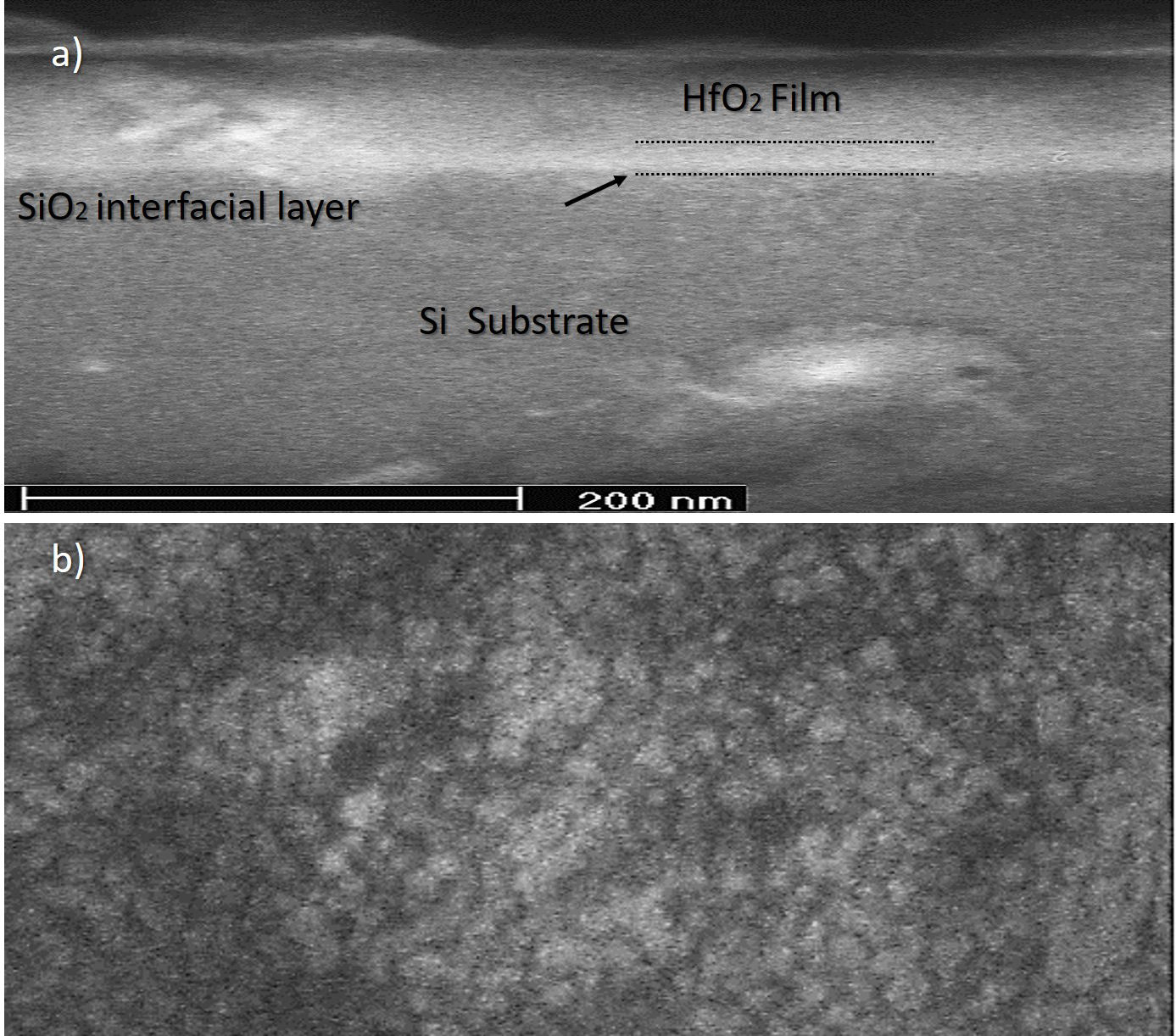
Figure 4a shows a transversal view of a WW deposited sample obtained by scanning electron microscopy. It is possible to visualize the different layers forming the structure, a first region corresponding to the Si substrate, a second region showing a SiO2 interface layer with a thickness of a few nanometers, related to the oxidation at the time of deposit (present in WoW and WW samples). A third region is related to the deposition of the HfO2 thin film [34]. Figure 4b corresponds to the HfO2 film surface, showing nanostructured crystals formation, in agreement with the GIXRD diffractograms and EDS measurements.
3.4. Atomic force microscopy
Atomic Force Microscopy shows the HfO2 thin film surface morphology (Fig. 5). For those samples obtained without water (Fig. 5a), as substrate temperature rises, the surface rugosity decrease from 19.8 to 5.79 nm (Table I), and the film quality enhances. The Hf(acac)4 thermal decomposition is more efficient, thus considerably reducing organic waste. The organic residues are more easily removed as the temperature increases. The metal part melts, forming mainly thin layers that create dense and compact films, thereby leading to low roughness surfaces.
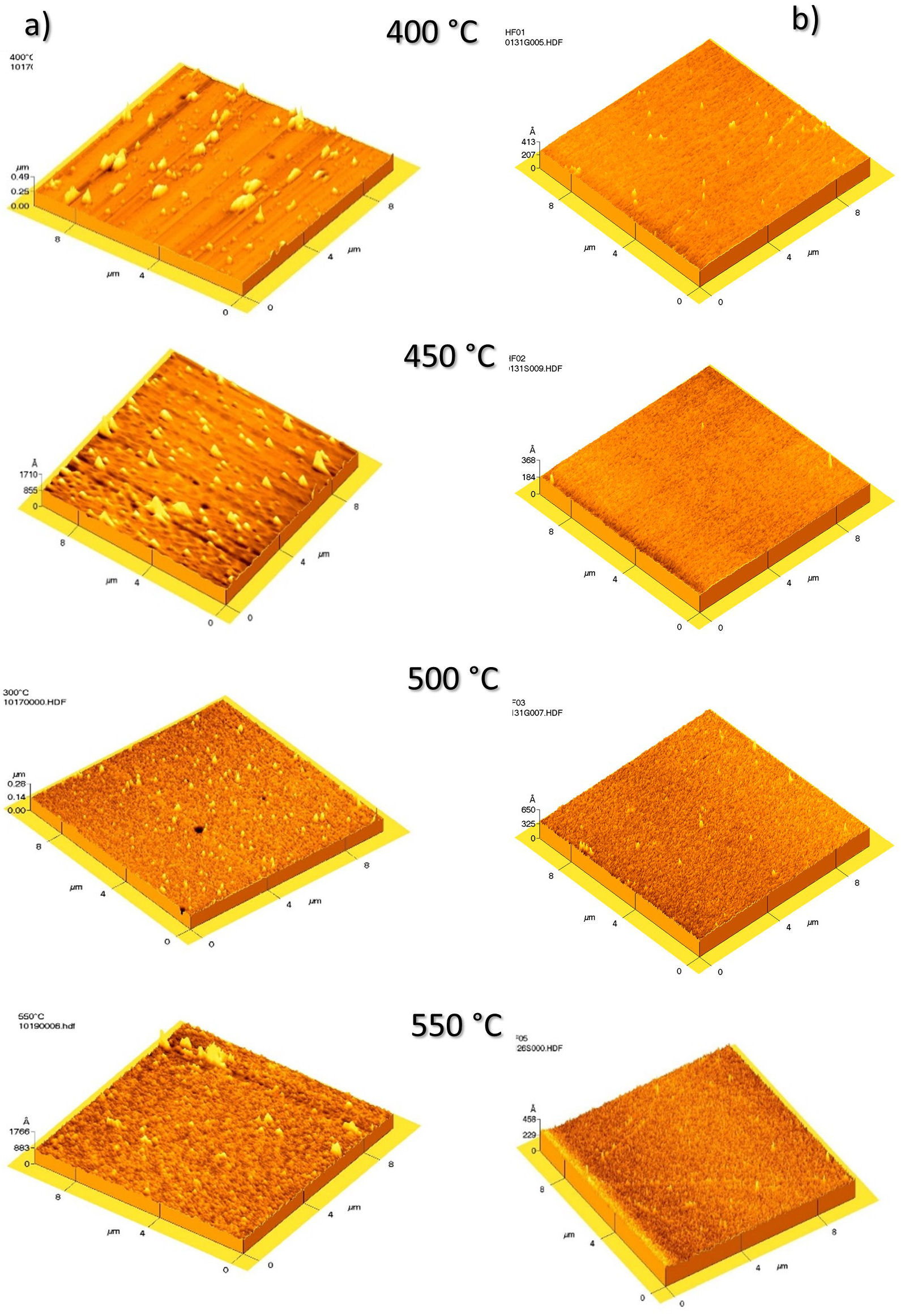
FIGURE 5 Atomic Force Microscopy shows the HfO2 thin film surface morphology, column a) WoW and column b) WW.
TABLE I Rugosity, thickness, refractive index, and packing density for WoW and WW samples.
| WoW samples | WW samples | |||||||
|---|---|---|---|---|---|---|---|---|
| Temperature | Rugosity | Films thickness | Refractive | Packing | Rugosity | Films thickness | Refractive | Packing |
| (°C) | (nm) | (nm) | index | density | (nm) | (nm) | index | density |
| 400 | 19.80 | 120.0 | 1.92 | 0.91 | 0.89 | 32.5 | 1.87 | 0.88 |
| 450 | 6.14 | 115.0 | 1.95 | 0.93 | 0.45 | 11.0 | 1.90 | 0.90 |
| 500 | 6.77 | 165.0 | 1.92 | 0.91 | 1.59 | 23.0 | 1.89 | 0.89 |
| 550 | 5.79 | 130.0 | 2.00 | 0.95 | 1.86 | 18.5 | 2.02 | 0.96 |
On the other hand, the samples deposited with water under the same conditions (Fig. 5b) have a lower rugosity than the WoW. This decrease in roughness could be because water flow dilutes the solution causing a smaller amount of material to reach the substrate surface. As there is less organic waste, the metallic part melts with the substrate, forming uniform thin layers, allowing a better structural arrangement. The increase in roughness with increasing temperature for WW samples is directly related to the increase in crystallite size discussed above (Fig. 3). Another factor to consider is the irregularities caused by the SiOx layer generated when the silicon wafer is exposed to the environment; the layer is not uniform, so the film takes the form of this interfacial layer. The film deposited at 450◦C has the lowest rugosity.
3.5. Infrared (IR) spectra analysis
IR analysis for WoW samples is shown in Fig. 6a. The films deposited at 400 and 450◦C present broadband centered approximately at 3400 cm−1 due to O-H type bonds [36,37]. This same band appears slightly on those films deposited at 500 and 550◦C. The bands located at 1510 and 1410 cm−1 correspond to vibrational modes of the asymmetric stretching of carbonyl CO(vas). It is also possible to appreciate two bands close to 1512 and 1595 cm−1 related to carbonyl groups. The Inset in Fig. 6 corresponds to a typical IR spectrum for Hf(acac)4, showing two bands at 1530 and 1595 cm−1 due to carbonyl groups. Therefore, those bands observed in our samples must be associated with carbon residues because of the source reagent incomplete decomposition [38].

FIGURE 6 a) IR spectra from WoW samples grown from 400 to 550◦C. Two bands close to 1512 and 1595 cm−1 related to the carbonyl groups, a band centered in 3400 cm−1 due to O-H bonds, are observed. b) IR spectra from WW samples. The bands related to the carbonyl groups disappear, O-H bonds noticeably decrease, and hafnium oxide bands are better defined. The Inset represents Hf(acac)4 IR spectra.
The bands located at 512, 635, and 752 cm−1 are reported for hafnium oxide with a monoclinic structure [39,40]. A small band located at approximately 750 cm−1 is observed in our spectra on those films deposited from 450 to 550◦C. The above indicates the existence of Hf-O type bonds, consistent with the GIXRD results, where a peak corresponding to the orientation (111) of the monoclinic phase is observed for those films.
On the other hand, WW films (Fig. 6b) do not present the band centered at 3400 cm−1, related to O-H type bonds. Then, if deionized water is added, there is a notable decrease in this type of bond. Additionally, the bands located around 1500 cm−1 appear with a lower intensity, indicating that these films are generally cleaner from carbon-associated residues [41]. Obtaining films with less carbon through water addition has already been observed in other types of films, such as aluminum oxide synthesized by LPCVD [42].
The function of deionized water steam is to promote carbon compounds desorption from the surface where the film growth occurs. WoW films at 400 and 450◦C present O-H bonds, which disappear when heated, but as soon as they cool and are exposed to the environment, they physisorbed water. This does not happen with WW samples exposed to the environment [41]. The hafnium oxide bands located at 512, 635, and 752 cm−1, seem to be very noticeable in almost all the spectra of Fig. 6b) [39,43]. It is observed that the band located at ∼ 500 cm−1 increases its intensity as temperature rises. For films deposited at 400◦C, the band located at 500 cm−1 is not very noticeable in the spectrum, but those films deposited at 450, 500, and 550◦C appear more intense.
3.6. Ellipsometry analysis
The thicknesses for each sample have been determined using ellipsometry (our results are presented in Table I). We have considered the average thickness evaluation in the calculations, considering the interfaces present in each of the structures as we observed from SEM (Fig. 4a). As it is observed, the thickness of WoW thin films is larger than those of WW. As we have previously mentioned, water helps to carry away those carbons left free when the salt melts, this makes the reaction slower, and a smaller amount of hafnium reaches the surface.
The refractive index was obtained employing a fixed wavelength ellipsometer. For WoW samples, the refractive index at 400 and 500◦C is n = 1.92 (amorphous phases), and at 450 and 550◦C, the values are n = 1.96 and n = 2.00, respectively, which are related to the crystallites formation with direction (002) and (111). For WW samples, the refractive index tends to increase slightly as temperature increases, consistent with the crystalline state behavior [44]. The refractive indexes acquired in this work are comparable with those obtained by Atomic Layer Deposition (ALD), with values between n = 1.8 and n = 2.0. Similar results are reported for light-assisted sol-gel synthesis, with a refractive index of n = 1.90 [45].
Moreover, the refractive index is related to the packing density p (dependent on the ratio of the volume of the solid part to the total volume of the film, which includes the pores), and it can be determined by the expression [46]
here n v is the void refractive index (n v = 1) and n s is the bulk refractive index (n s = 2.1). The corresponding values are reported in Table I. The packing density for the WoW samples is associated with the OH bands present in the IR analysis, induced by moisture adsorption from the thin film in the environment, presenting a variation on the refractive index (or packing density) [47,48]. On the other side, for WW samples, there is a strong correlation with GIXRD when the crystalline structure is better defined. There are slight packing density changes for samples at 400-500◦C; however, the packing density increases abruptly for the 550◦C sample. As the temperature increases, a better structural arrangement is generated, voids and structural defects are reduced, causing a shrinkage that affects the film thickness, and, consequently, the packing density increases [49]. Furthermore, the Hf/O ratio decreases notably for this temperature, consistent with EDS observed behavior.
3.7. C-V analysis
Figure 7 shows the C-V curves for the MOS structures made with HfO2 films (WW samples) at different temperatures. The curves have been normalized to make a better comparison and determine the effect of temperature and water-assisted deposition on their electrical properties. The film grown at 400◦C has an accumulation region at 1490 pF and a dielectric constant of 13.8; the inversion zone tends to be vertical and close to zero, presenting a slight shift to the left, related to fixed insulating loads due to a high oxygen concentration, possibly caused by the formation of the SiOx interfacial layer [54]. There is a small hump, characteristic of slow traps present at the insulator/semiconductor interface, due to defects distributed outside the insulator interface. Therefore, the emission and capture of electrons produce a constant dispersion over time, giving rise to hysteresis in the C-V curve [55]. The graph corresponding to 450◦C is the most representative of a MOS structure since the C-V curve is the best defined, with a slight shift to the left, and whose accumulation region presents a value of 1406 pF. The absence of shoulders indicates few defects and traps at the interface, showing that the C-V response is expected for an ideal dielectric material, with a dielectric constant of 14.4 [50-52]. We obtained the highest dielectric constant value and the best electrical properties for this sample than for all the synthesized samples. For samples grown at 500◦C, the behavior is not typical for a MOS structure; the inversion part is slightly curved, reaching a maximum of 1229 pF and a dielectric constant of 8.5; the inversion zone has a hump. Finally, the C-V curve for the 550◦C sample is the one with the least expected behavior; it is deformed, the accumulation tends to be flat over 170 pF, well below the previous samples [53]; the inversion and depletion zone is not adequately defined.

FIGURE 7 C-V normalized curves of the MOS structures made with HfO2 WW films (WW samples) deposited at different temperatures.
The electrical characteristics of WoW samples are not suitable for C-V calculations. This can be attributed to the SiO2 thermal layer (up to 100 Å) between the silicon substrate and the HfO2 film. In addition to its high thickness, the defects contribute to generating a poor electrical response. The high quality of the WW films minimizes the effect of the SiO2 layer. This problem is still presented by films deposited by sophisticated techniques such as ALE. When HfO2 is deposited on other materials, this problem does not arise.
4. Conclusions
We have presented the effect of deionized water-assisted synthesis of HfO2 from Hf(acac)4 by the ultrasonic pyrolytic spray technique. Our results show that vapor water favors the formation of polycrystalline films with a well-defined monoclinic phase at specific temperatures. Samples grown without the addition of deionized water are amorphous and with low structural order. The carbon and O-H bonds decrease considerably, making thinner films than those deposited without water and better controlling the HfO2 film growth. Films deposited at 450◦C have the highest dielectric constant (14.4) and do not exhibit hysteresis, in contrast to the other films; moreover, roughness has a minimum value (0.45 nm) for this sample. Therefore, the effect of deionized water during deposition on HfO2 films improves the structural, optical, and electrical characteristics, making them compact and nanostructured.
We have shown that water-assisted ultrasonic spray pyrolysis is an excellent method to synthesize HfO2 thin films (from metal-organic precursors) with appropriate structural optical and electrical properties for the fabrication of ultralarge-scale integration systems and technological applications such as MOSFET, CMOS, NVM, RAM card, and other devices.

