


 nueva página del texto (beta)
 Inglés (pdf)
 Artículo en XML
 Referencias del artículo
 Enviar artículo por email
 Citado por SciELO
  Similares en
SciELO
Similares en
SciELO 
 Permalink
1.Introduction
There are three main phases of copper oxide: tenorite (CuO), cuprite (Cu2O), and paramelaconite (Cu4O3) 1-3. The last crystallizes in a tetragonal crystal structure and has a unit cell with three lattice parameters: a = 5.8370 Å, b = 5.8370 Å, and c = 9.9320 Å4. Cu4O3 is a p-type semiconductor and has a bandgap of 1.75 eV 5. Although is a metastable phase, it has been recently used in combined with other compounds in some important applications. For example, it has been used in improving catalytic activity of copper oxide-based catalysts 6, as a p-type layer in the fabrication of photodetectors 5, and in antibacterial and cytotoxicity studies 7. Although Cu4O3 can be produced by several techniques such as solvothermal synthesis 8, laser ablation 9, or reactive sputtering 10, it is known that it is difficult to synthesize Cu4O311,12. Copper oxide thin films can be easily deposited by reactive sputtering using metal copper targets 13,14. A single phase of CuO, Cu2O, or Cu4O3 can be formed by controlling the oxygen flow rate in reactive magnetron sputtering deposition 10. In the present report, crystalline Cu4O thin films were obtained by non-reactive rf magnetron sputtering using a home-made copper oxide target, fabricated by thermal oxidation of a metal copper disk.
2.Materials and Methods
Cu4O3 thin films were deposited on glass substrates by non-reactive rf magnetron sputtering. The copper oxide targets were fabricated by thermal oxidation of electrolytic copper (C-1100, purity of 99.9 %) disks (two inches of diameter and 500 μm in thickness) (Fig. 1a). Previous to oxidation, the metal copper disks were rinsed in acetone (10 min) and then in ethanol (10 min). Then, they were oxidized at 1000oC for 24 h in the ambient atmosphere using a Thermo-Scientific Thermolyine muffle furnace, model FB1415M. The metal copper disks were placed into the muffle from room temperature to 1000, and after oxidation, they were cooled naturally. The thickness of the copper oxide disks was 900 μm (measured with a Mitutyoyo micrometer, model H-2780). The surface of the oxidized disk exhibited the characteristic color of CuO (Fig. 1b). For sputter deposition of copper oxide, the applied voltage and current were 412 V and 8.9 mA, respectively. The copper oxide disc was sputtered in a LEICA MED-020 sputtering system, using Ar plasma at a system pressure of ∼6.1 x 10⁻² mbar. The duration of deposition was 1300 s, and corning glass was used as substrate. The thickness of the sputtered copper oxide thin film (Fig. 1c and 1d) was 370 nm, which was measured using a Sloan Dektak IIA profilometer.
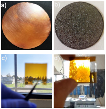
Figure 1 a) Photograph of a metal copper disk used for fabrication of the copper oxide target, b) copper oxide target obtained by thermal oxidation of copper, c) and d) top-view of the Cu4O3 thin film deposited by non-reactive rf magnetron sputtering.
X-ray diffraction (XRD) measurements were performed with a Bruker D8 Advance diffractometer with radiation of CuKα (1.5406 Å). Raman measurements were recorded sing a micro-Raman Horiba Jobin Yvon system (Xplora plus model). A laser (λ= 532nm) was used to induce scattering, using a maximum laser power of 10 percent. The laser beam was focused using a 100x lens and also it serves to recollect scattered light. A 600 lines/mm grating was employed; 100 acquisitions were averaged with an exposure time of 5 s each.
3.Results and discussion
3.1.Copper oxide target
XRD pattern of copper oxide target fabricated by thermal oxidation of copper at 1000 for 24 h in the ambient atmosphere is shown in Fig. 2. The 15 peaks observed in the XRD pattern indicate a polycrystalline structure. There are 12 diffraction peaks, at 2θ = 32.51, 35.59, 38.76, 46.24, 48.66 , 53.36, 61.53, 65.85, 68.16, 72.40, 75.26, and 80.18, which match with the (-110), (002), (111), (-112) (-202), (020), (-113), (022), (-220), (311), (-222), and (-204) planes, respectively, of CuO (PDF 00-045-0937). There are also three peaks at 2θ = 36.65, 42.18, and 73.43 which correspond to the (111), (200), and (311) planes, respectively, of Cu2O (PDF 00-005-0667). No peak are corresponding to metal copper. The structure of the disk is thus composed of a mixture of CuO and Cu2O crystals, which is commonly observed in growth, synthesis, or even in thin film deposition of copper oxide by different methods such as thermal oxidation or sputtering 14,15. Table I shows the full width at half maximum (FWHM) values calculated for all diffraction peaks observed in the XRD pattern of Fig. 2. The value of the FWHMs for peaks of the CuO phase are in the range of 0.06551-0.21978, and those of the Cu2O phase in that of 0.19098-0.25649. FWHMs for nanostructured CuO or CuO thin films have been previously found in higher values than those reported here, which indicates that the bulk of the copper oxide disk exhibits a crystalline structure 16,17.
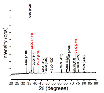
Figure 2 XRD diffractogram of a copper oxide target, formed by thermal oxidation at 1000±C for 24 h in air atmosphere.
Table I FWHMs calculated for the fifteen peaks of the XRD pattern of the copper oxide target, formed by thermal oxidation at 1000±C for 24 h in the air atmosphere
| Plane | ||||||||||||
| CuO | (-110) | (002) | (111) | (-112) | (-202) | (020) | (-113) | (022) | (-220) | (311) | (-222) | (-204) |
| FWHM | 0.13307 | 0.14777 | 0.21978 | 0.20723 | 0.16603 | 0.19891 | 0.08673 | 0.16729 | 0.09425 | 0.06551 | 0.12098 | 0.09934 |
| Cu2O | (111) | (200) | (311) | |||||||||
| FWHM | 0.25649 | 0.19098 | 0.19586 | |||||||||
Raman measurements were performed at three different zones of the copper oxide disk (Fig. 3a). The zone labeled as z1 indicates any point through the surface of the copper oxide disk. Raman spectrum of z1 is shown in Fig. 3b. There are three sharp bands centered at 294, 342, and 628 cm-1, which agree with the three Raman active modes (Ag + 2Bg) of CuO 18. Also, there a weak broadband of about 100 cm-1, which has been previously associated non-stoichiometry and defects in Cu2O 19,20. Thus, the surface of the copper oxide disk is mainly composed of CuO. The z2 label indicates a measurement zone into the disk at a depth of about 150 μm. There are two Raman bands centered at 143 and 214 cm-1, which correspond to Cu2O modes 21. There is also a broad and weak CuO band at around 628 cm-1. The Raman spectrum obtained by measuring at a depth of about 250 μm (z3 zone) exhibits the same three bands observed in the z2 zone. Thus, according to XRD and Raman measurements, the bulk of the copper oxide target is mainly composed of Cu2O and a surface crystalline layer of CuO.
3.2. Cu4O3 thin films
Copper oxide thin films were deposited by non-reactive rf-magnetron sputtering.
According to XRD and Raman measurements performed to the copper oxide target,
the deposition was achieved by sputtering to the CuO layer on the surface of the
copper oxide disk. XRD pattern of sputtered copper oxide thin film is shown in
Fig. 4. There are only two peaks at 2θ
= 43.66 and 63.97, which correspond to (220) and (400) planes, respectively, of
the phase of copper oxide (PDF 00-033-0480). The FWHM of the (220) peak
(0.33696) is smaller than that of (400) peak (0.73691), which indicates that the
average crystal size (estimated by the Scherrer equation) is higher for the
(220) peak than that of the (400) peak (26.52 and 13.27 nm, respectively) 22. Also, since the intensity of
the (220) peak is about six times higher than that of the (400) one, the thin
film exhibits a preferred orientation along the (220) plane. The broadband from
2θ = 14o to 2θ = 37o is the characteristic amorphous band
of the glass substrate. This band appeared due to the low thickness of the
Cu4O3 film. The structural characteristics of the
copper oxide target and thin films are shown in Table II. For crystal size calculation using the Scherrer equation
(
where n is a factor, which gives the minimum dislocation density when is equal to
unity. The distortion degree by variation of the d-spacing within or between
crystal domain was calculated by microstrain (
Table II Crystallite size, dislocation density, and micro-strain of the copper oxide and the Cu4O3 thin films.
| Sample | D(nm) | δ x10-4(nm-2) | ε x 10-4 |
| Copper oxide target | 54.89 | 3.318 | 20.698 |
| Cu4O3 this film | 26.52 | 16.126 | 37.468 |
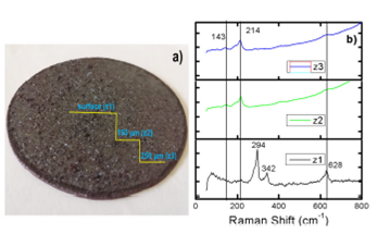
Figure 3 a) Photograph of the copper oxide disk where the depth profile used for Raman measurements is observed. b) Raman spectra of measurements performed at the surface and in the bulk of the copper oxide disk.
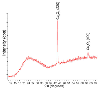
Figure 4 XRD pattern of the Cu4O3 thin film deposited by nonreactive rf magnetron sputtering of copper oxide.
It can be observed that Cu4O3 thin films exhibit a smaller crystal size than the copper oxide target, and, consequently, an increment in the microstrain and dislocation density is produced during the formation of the Cu4O3 thin films.
Raman spectra of the Cu4O3 thin film was performed in three different zones: at the top (point2), at the center (center), and at the bottom of the surface of the thin film (point1) (inset of Fig. 5). There are five main Raman modes in each spectrum of Fig. 5, although peak positions, intensities, and the width of the bands are not identical in all spectra. These variations suggest that the composition of the thin film is inhomogeneous across all its surface. The peak of about 213 cm-1 corresponds to Cu2O mode 25. The peaks of about 272 and 603 cm-1 correspond to CuO modes 26. The peaks about 323 and 545 cm-1 correspond to Cu4O3 modes 27.
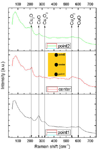
Figure 5 Raman spectra of the Cu4O3 thin film deposited by non-reactive rf magnetron sputtering of copper oxide. Measurements were performed at three points of the surface of the film (inset): at the the top (point2), at center (center), and the bottom (point1).
XRD results showed a pattern exhibiting only Cu4O3 peaks, and Raman measurements suggest that a mixture of CuO, Cu2O, and Cu4O3 phases are present in the structure of the thin film. The bands of the three phases of copper oxide (CuO, Cu2O, and Cu4O3) observed in Raman spectra of the thin film deposited by non-reactive rf-magnetron sputtering are very broad, particularly those that were obtained from the “center” and the “point2” zones. This may be associated with a poor crystalline quality of the thin films.
4.Conclusions
Cu4O3 thin films were deposited by non-reactive rf-magnetron sputtering using a copper oxide target, which was obtained by thermal oxidation of copper. From XRD and Raman analyses, deposition of the Cu4O3 thin films was achieved by sputtering to the surface CuO layer of the target. XRD measurements indicated that only crystals are present in the structure of the thin films. However, the broad bands of CuO and Cu2O observed in Raman spectra revealed a bulk composed of a mixture of the three copper oxide phases.

