


 nova página do texto(beta)
 Inglês (pdf)
 Artigo em XML
 Referências do artigo
 Enviar este artigo por email
 Citado por SciELO
  Similares em
SciELO
Similares em
SciELO 
 Permalink
1. Introduction
The functionality of a field effect transistor with low operating voltage and high carrier concentration depends on the semiconductor channel layer material and the dielectric gate amidst other parameters because a transistor’s threshold voltage (Vth) depends on the semiconductor material [1].
However, so far only oxides, nitrides, carbon nanotubes and organic semiconductors have realized the recorded modulation of electronic states in a field effect transistor. The application of the electric double layer field effect transistor (FET) technique to other groups of semiconductors is of wide interest for its performance on novel devices [2]. Tin (II) sulphide (SnS) is of interest as a semiconductor channel layer for transistors. SnS is a readily available Tin chalcogenide layered semiconductor in group IV-VI with a layered orthorhombic structure [3]. SnS contains no poisonous or costly elements; it is of type p with a hole mobility of 1.4 cm2 V−1s−1 and carrier concentration on the order of 1016 cm−3 [4]. SnS thin film is largely unexplored for use in field effect transistors as the literature relating to the use of SnS as a semiconductor channel layer is relatively scarce.
Therefore, SnS thin film is a worthy material to investigate the feasibility of the chalcogenide family for a field effect transistor’s channel and to determine the optimum deposition parameters that will provide the required properties for its usage. Thin film thickness, which is a function of the film microstructure, is a parameter of interest. In semiconductor processing, the regulation of film thickness is critical as the film thickness influences the grain size and grain boundary which is necessary for defining the electrical properties of a semiconductor material [5]. Voids in a separate island-like state and traps associated with certain film thickness affect charge carriers due to the number of small grains with large quantities of grain boundaries acting as an electron trap, affecting an SnS film’s electrical conductivity and the threshold voltage for use in a FET.
The method of deposition of interest is the aerosol assisted chemical vapour deposition (AACVD). AACVD provides the comparative benefit of using less-volatile precursors, thus increasing the types of molecules which can be used to deposit thin films. For the field effect transistor a 0.20-0.40 µm thickness range was selected based on the average values gotten from the literature.
2. Experimental procedure
Preliminary deposition and film thickness measurements were performed to establish the concentrations of the starting precursor. SnS semiconductor thin films were deposited using 0.1 M Tin chloride dehydrates and 0.2 M of Thiourea which were weighed in stoichiometric proportion and dissolved in ethanol solvent. The two solutions were mixed and stirred for 1 hour using a magnetic stirrer at room temperature after which the resulting solution was filtered through a 0.22 µm syringe filter and then deposited on the substrate by AACVD at a constant substrate temperature of 258◦C, nozzle distance of 6.8 mm, substrate to nozzle distance of 3 cm, spray volume of 0.2 mL and spray rate of 0.04 ml/min. Five samples of SnS thin films were deposited at thickness of 0.4 µm, 0.35 µm, 0.30 µm, 0.25 µm and 0.20 which was achieved by keeping the initial concentration of the SnS precursors constant using 1 ml of the precursor while varying the concentration of the ethanol solvent through 0 ml, 0.5 ml, 1.0 ml, 1.5 ml, and 2.0 ml.
Structural characterisation of the films was carried out at room temperature using an X-ray diffractrometer (D8 Advance, Bruker AXS, 40Kv, 40 mA) with monochromatic CuKα (λ = 1.540598 Å) while phase identification was done using the inorganic crystal structure data pattern [6].
The average crystallite size (D) of the film was calculated using Debye Scherer’s formula:
where β full width at half maximum (FWHM), θ diffraction angle, k Shape factor and λ wavelength of the X-rays (1.5406 Å).
Dislocation density δ was calculated using [7]:
and the micro-strain ε was estimated using the equation [8,9]
The morphology and microstructure of the SnS thin films were characterized using High Resolution Scanning Electron Microscopy (HR-SEM, Zeiss) while the elemental composition of the film was determined by an Energy dispersive X-ray spectroscopy (EDS; Oxford instrument). A Profilometry (VEECO DEKTAK 150) was used to carry out measurements of the thickness of the deposited films. The carrier density, carrier mobility and carrier type were determined by an ECOPIA Hall Effect measurement system (HMS 3000 Hall measurement system) based on a Van der Pauw configuration.
3. Results and discussion
3.1. Compositional analysis of As-deposited SnS thin films
The thickness of the as deposited SnS thin films as-obtained from surface profilometry were 0.20 µm, 0.25 µm, 0.30 µm, 0.35 µm and 0.40 µm. Figure 1 displays the EDS spectrum of the as-deposited SnS thin films, while the elemental composition of the SnS films is shown in Table I in terms of their atomic percentage. Sn and S were found to be dominant in SnS thin films, while small quantities of sodium (Na), calcium (Ca), silicon (Si), oxygen and chlorine (CI) were also found in films that could be linked to the soda lime glass substrate used for film deposition which was similarly reported by [10]. From Table I, it was observed that the Sulphur content increased with increased film thickness. Lower film thickness compared to higher thickness has lower Sulphur content.
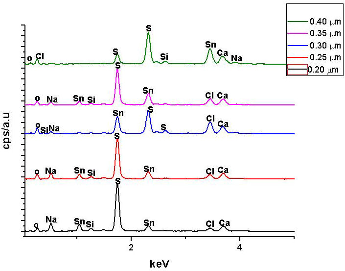
FIGURE 1 EDS spectrum of the SnS thin films of 0.20 µm, 0.25 µm, 0.30 µm, 0.35 µm and 0.40 µm thickness.
TABLE I As-deposited SnS thin film composition in terms of atomic percent (at.%).
| Thickness (µm) | Sn (at. %) | S (at. %) | Ca (at. %) | Na (at. %) | Cl (at. %) | Si (at. %) | O (at. %) | TOTAL 100 |
| 0.20 | 36.43 | 45.57 | 8.35 | 1.04 | 5.62 | 1.74 | 1.25 | 100 |
| 0.25 | 35.72 | 46.28 | 8.35 | 1.04 | 5.62 | 1.74 | 1.25 | 100 |
| 0.30 | 33.19 | 48.81 | 8.35 | 1.04 | 5.62 | 1.74 | 1.25 | 100 |
| 0.35 | 30.75 | 51.25 | 8.35 | 1.04 | 5.62 | 1.74 | 1.25 | 100 |
| 0.40 | 29.85 | 52.15 | 8.35 | 1.04 | 5.62 | 1.74 | 1.25 | 100 |
Since Sulphur has a greater vapour pressure compared to Tin, more of the Sulphur atoms will arrive on the substrate compared to Tin atoms as observed in Table I. Some of the Sulphur atoms appear to be reflected back on arrival at the substrate surface which could be due to adsorbed-atom mobility, lower sticking coefficient or heat radiant effect between the substrate surface and the deposited SnS thin film resulting in lower Sulphur content or a significant deficiency at lower thickness than higher thickness. However, the effect decreases at higher thickness due to the drop in the loss of scattering leading to a decline in heat gradient with the formation of clusters of SnS crystallites at higher SnS thin film thickness which is consistent with the report of Ref. [11].
3.2. X-Ray Diffraction
Figure 2 shows the XRD pattern of SnS thin films of 0.20 µm, 0.25 µm, 0.30 µm, 0.35 µm and 0.40 µm thickness scan over the range of 20◦ ≤ 2θ ≤ 80◦. The peaks observed for the films were analysed and indexed using the standard pattern with orthorhombic structured SnS (JCPDS PDF card 39-0354) for the mineral herzenbergite. Analysis of the films’ XRD pattern shows the formation of a loosely crystalline film because of the presence of few peaks. The films of 0.20 and 0.25 µm thickness showed only one peak at a 2θ value of 31.7◦ diffracted along the (040) plane that appears as a single crystal in nature or a single broad, poorly crystalline peak with other peaks fully suppressed, which could be due to the ordering of short range between the atoms at the thickness level and is peculiar to chalcogenides deposited at room temperature of low crystallinity or an almost amorphous nature [12]. The SnS thin films of 0.30, 0.35 and 0.40 µm thickness, however, showed few peaks at 2θ approximately 31.7◦ and 66.6◦ diffracted along the plane (040) and (080) respectively, indicating an increase in atomic order with increase in film thickness. There is no difference in films peak position with thickness increase; but there is an increase in intensity with a rise in film thickness. The broad peak located at a small angle of diffraction is unique to the amorphous network. The full width half maximum of the peaks were estimated using a Gaussian function via the use of OriginPro 2015 software. The summarised structural parameters of the films is given in Table II.
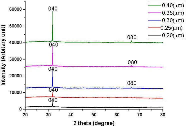
FIGURE 2 XRD pattern for SnS thin films of 0.20 µm, 0.25 µm, 0.30 µm, 0.35 µm and 0.40 µm thickness.
TABLE II Summary of calculated structural parameters for different SnS thin film thickness.
| S/n | Thickness (µm) | 2θ (◦) | Full width half maximum β (◦) | Crystal size D (nm) | Dislocation density δ ×1014 (Lines/m2) | Micro strain ε ×10−3 |
| 1 | 0.40 | 31.739 | 0.136 | 60.72 | 2.71 | 2.09 |
| 2 | 0.35 | 31.742 | 0.139 | 59.41 | 2.83 | 2.13 |
| 3 | 0.30 | 31.757 | 0.143 | 57.75 | 3.00 | 2.19 |
| 4 | 0.25 | 31.703 | 0.146 | 56.56 | 3.13 | 2.24 |
| 5 | 0.20 | 31.702 | 0.150 | 55.05 | 3.30 | 2.31 |
The average size of the crystallites was estimated using the full width at half the maximum of the most preferred orientation (040), which is also the Scherer formula’s most extreme value. The average size of crystallites was found to increase with increase in the thickness of the SnS thin films. Increasing the film thickness facilitates the formation of grown atomic layers, creating a thermal energy gain system which enhances atomic restructuring leading to an increase in the crystal size and a decline in crystal defects in the SnS thin films. From Table II, the decline in full width at half maxima with increase in the film thickness represents the decrease in the amount of lattice imperfections in the deposited SnS thin film due to a substantial decrease in the SnS thin film’s internal micro strain. The average crystallite size of the films increased from 55.05 nm to 60.72 nm with a film thickness increase from 0.2 to 0.40 µm. The low value of 55.05 nm for the lower thickness of 0.2 µm could be attributable to a decline in the growth of deposited SnS film atoms due to a reduction in nuclide formation caused by the insufficiency of material and bonding between the nuclides and the substrate surface which could limit the mobility of deposited atoms inpart. However, nuclide formation significantly increases with increase in SnS film thickness and a decrease in the interactions between the substrate surface and the deposited film layer, thereby resulting in the merger of smaller crystallites into larger ones as a consequence of the potential energy gap between small and large particles. Similar results were published in [13,14]. Increase in film thickness increases the size of crystallite by forming larger grains on the surface of smaller grains [15]. The thickness of 0.40 µm has the largest size of crystallite, and could therefore be the most crystalline. The decline in micro strain and dislocation density with increased film thickness could be due to the stress release in SnS thin films by simultaneous growth annealing phenomenon contributing to improved film crystallinity with increase in the SnS thin film thickness.
3.3. Scanning electron microscopy (SEM)
Figure 3 (a-e) shows the surface morphology of the 0.2, 0.25, 0.30, 0.35 and 0.40 µm thickness of as-deposited SnS thin films as investigated with SEM. Using imagej software [16], the average grain size of the SnS thin films was computed.
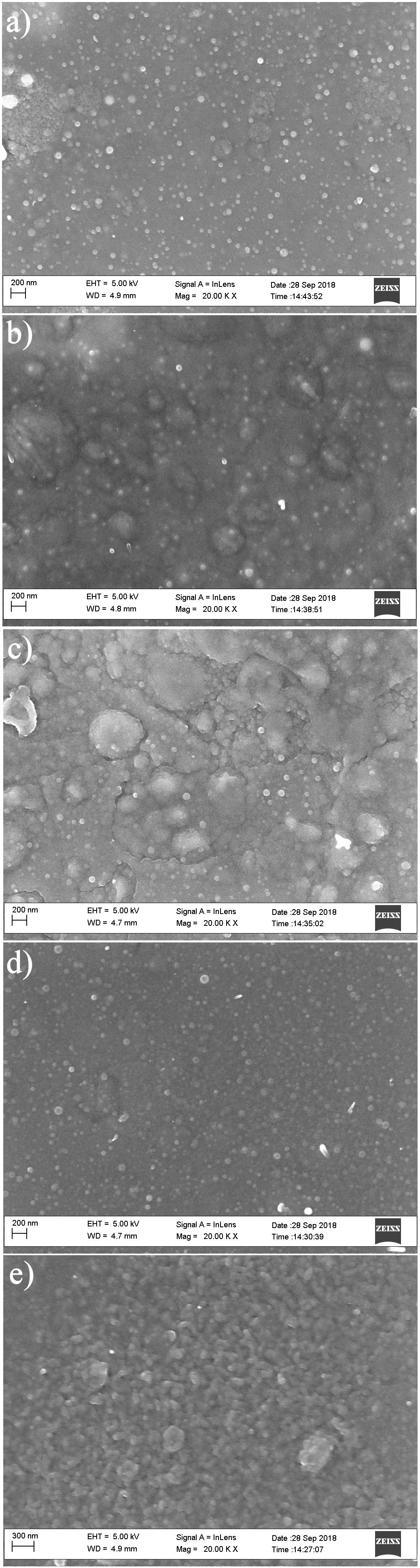
FIGURE 3 (a-e). The surface morphology of the as-deposited SnS thin films of 0.2, 0.25, 0.30, 0.35 and 0.40 µm thickness.
The SnS thin films of 0.2 to 0.40 µm thickness exhibited two distinctive microstructures consisting of a section of agglomerates and some defined spherical grains as shown in Fig. 3. The agglomerates increase for films of 0.2 to 0.30 µm thickness after which they decrease for films of 0.35 to 0.40 µm thickness resulting to a more specified grain structure and growth of SnS thin film of 0.40 µm thickness. The 0.2 to 0.30 µm thickness of the SnS films displayed uniformly spaced grain sizes. No visible crack or hole was observed in the deposited SnS thin films as the films were located randomly on the SnS film surface. With increase in SnS film thickness to 0.35 and 0.40 µm, the films contain more uniform and closely bound grains such that the film of 0.40 µm thickness possess the most enhanced grain and crystal structure. In addition, with increase in film thickness, the deeper layers of the film atoms are exposed to stronger interatomic forces leading to the creation of a compact structure, while the atoms near the surface are subjected to weaker interatomic forces to form a loosely packed grain structure for a thinner film [12,15]. Figure 4 displays the composite average grain size plot for thicknesses of 0.2, 0.25, 0.30, 0.35 and 0.40 µm.

FIGURE 4 Composite average grain size plot for 0.20, 0.25, 0.30, 0.35 and 0.40 µm SnS thin film thickness.
Figure 4 shows that, with increase in the SnS thin film thickness, the average grain size as labelled on each column increases. The increase in thickness allowed the growth of smaller grains into larger grains that could be credited to the coalescence of small grains into larger grains with an apparent change in the more tightly packed grain size of the SnS thin film.
3.4. Hall effect measurement of 0.20, 0.25, 0.30, 0.35 and 0.40 µm SnS film thickness
The electrical properties of the as deposited SnS thin film as a function of film thickness is shown in Table III.
TABLE III Electrical parameters of SnS thin films of 0.20, 0.25, 0.30, 0.35 and 0.40 µm SnS film thickness.
| Thickness (µm) | Bulk concentration Nb (cm−3) | Average Hall coefficient RH (cm3/c) | Carrier mobility µ (cm2/Vs) | Resistivity ρ (Ωcm) | Conductivity ρ (Ωcm)−1 |
| 0.20 | 2.572 ( 109 | 2.224 ( 109 | 5.257 ( 102 | 4.230 ( 106 | 2.364 ( 10-7 |
| 0.25 | 2.807 ( 109 | 2.427 ( 109 | 9.132 ( 102 | 2.658 ( 106 | 3.762 ( 10-7 |
| 0.30 | 2.990 ( 109 | 2.642 ( 109 | 1.714 ( 103 | 6.081 ( 105 | 1.645 ( 10-6 |
| 0.35 | 1.438 ( 1010 | 4.342 ( 109 | 2.063 ( 103 | 4.085 ( 105 | 2.448 ( 10-6 |
| 0.40 | 2.238 ( 1010 | 6.928 ( 109 | 4.337 ( 103 | 3.612 ( 105 | 2.768 ( 10-6 |
From the table, the average Hall coefficient of all the deposited SnS thin films was found to be positive, which means that all the films possess conductivity of the p-type carrier. A similar form of thin film conductivity was reported by [1820] among others for thin films of SnS. Several researchers have reported variations in the electrical resistivity of deposited SnS thin films to depend on lattice defects (e.g. interstitials, vacancies and the presence of binary film phases), residual stress, and grain size. However, no binary phases of SnS film have been found from the EDS studies but the grain size of the deposited films increases with thickness increase [12,15,18,19]. Therefore the difference in electrical conductivity with thickness may largely be due to the grain size of the films. The high resistivity of 0.20 and 0.25 µm thickness for thin films may be due to the existence of higher number of lattice defects, low crystallinity and the existence of inter-crystalline regions affecting grain growth to a relatively large scale. A further increase in thickness from 0.30 µm to 0.40 µm leads to a progressive change of the film crystallinity resulting in a more uniform structure with comparatively larger grains. The larger grains minimize the number of grain boundaries and trap density thereby enabling the carriers to move freely in the lattice resulting in reduced resistivity and increased film conductivity. The presence of defects acts as scattering centres for thinner films that could improve the creation of trap states capable of trapping carriers and the number of free carriers available for conduction. After trapping mobile carriers, the carrier traps may become electrically charged by generating a possible energy barrier that hinders the movement of charge carriers from one crystallite to another, thus reducing carrier mobility and the number of available carriers available for electrical conduction [14,15].
4. Conclusion
The SnS thin films deposited by AACVD were found to be polycrystalline consisting of Sn and S elements in varying composition. The presence of large grain size with increases in the SnS film thickness from 0.20 µm to 0.40 µm reduces the number of grain boundaries and charge trap density, hence allowing charge carriers to move freely in the lattice leading to a reduction in resistivity and an increase in conductivity of the film. This also reveals that the attainment of the threshold voltage of a transistor is proportional to the conductivity of the semiconductor channel layer which is a function of the presence of grain size and grain boundary interactions within the semiconductor channel layer. The high carrier concentration of 1.438×1013 cm−3 due to low resistivity of 3.612×10⁵Ωcm of 0.4 µm SnS thin film is optimum and favours the attainment of the threshold voltage for a transistor operation, hence it indicates the possibility of usage or application of SnS thin film as a semiconductor channel in a field effect transistor at an optimum charge carrier conductivity of 2.768×10⁻⁶ (Ωcm)−1, 0.4 µm thickness and 130.31 µm grain size.

