


 nueva página del texto (beta)
 Inglés (pdf)
 Artículo en XML
 Referencias del artículo
 Enviar artículo por email
 Citado por SciELO
  Similares en
SciELO
Similares en
SciELO 
 Permalink
1.Introduction
The group III-nitride semiconductors have aroused the interest of experimenters as well as theoreticians 1 29, such as Gallium nitride and indium nitride and their solid solutions are III-V semiconductor that gained significant attention for constructing multi Quantum well based optoelectronic devices: laser diodes and light-emitting diodes 5. To optimize and exploit the potential of the GaN and InN for further optoelectronics applications and solar cell technology, superlattices (SL s ) are one of the simplest ways to tailor the electronic and optical properties of the materials. Especially, it has been shown that SL s systems can be very useful for theoretical investigation. The cause for that is that atomic monolayers of GaN and InN in InN/GaN S L8 are grown separately and with the wanted width for each layer. It is found in literature many studies showing InN/GaN system make the design of various InN-based heterostructure devices possible 6 11. Indeed, its bandgap can cover the whole solar spectrum solely by changing the number of GaN monolayers in InN/GaN SL s 12,15. It is well known that crystal orientations have a significant impact on their properties and their potential applications. They can be generated artificially during the growth process, but they can also occur naturally since a change of orientation can be induced by temperature or pressure 16,18.
For lattice-matched heterostructures, the (110) orientation is particularly simple to handle (zinc-blende-type crystals) since the interface is nonpolar. For strained-laye SL’s, on the other hand, a theoretical description becomes substantially complicated because the atoms do not necessarily stay in planes perpendicular to the growth direction. The interface can then become polar 20. Therefore, one expects qualitative differences between the energetics of (110) growth and growth in all other orientations 20. In recent years, there has been some experimental 21 24 and lots of theoretical research conducted on the physical properties of III-compounds SL s , oriented along the (110). I. Gorczyca et al. 29 have investigated the electronic structures of the composition InN/GaN by comparing three different orientations of the growth direction in wurtzite phase by using the self-consistent ab initio calculations based on the density functional theory (DFT). I. Gorczyca et al. 8 have investigated the bandgap behavior based on first-principles calculations of electronic band structures for various short period nitride SL s . It is shown that for SL s , it is possible to exceed by far the range of band gap values, which can be realized in ternary alloys. G. Staszczak et al. 30 studied the measurements of photoluminescence and its dependence on hydrostatic pressure, which are performed on a set of InN/nGaN SL s along the growth axis (001), with one InN monolayer and with different numbers of GaN monolayers. It has been found that the transition energies for SL s are significantly higher than the calculated band gaps for the same kind of SL s . However, to our knowledge, the (InN) m /(GaN)n 𝑆𝐿′𝑠 with various growth axis directions have been given less or no attention. Our aim here is to investigate the symmetry of (110)-oriented SL s but also to give all the details concerning the (001) symmetries. The goal is to be able to predict the detailed electronic and optical characteristics of SL s grown along (001) and (110) direction using first principles calculations whose is devoid of adjustable parameters and can help shed light on different aspects of the problem. The paper is structured as follows. The computational method we have adopted for the calculations is briefly described in Sec. 2. The most relevant results obtained are presented and discussed in Sec. 3. Finally, in Sec. 4, we summarize the main conclusions of this work.
2.Detail of calculation
In the present study, the structural and electronic properties of binary InN and GaN compounds and their (InN)/(GaN) n superlattices are investigated using the first-principles full potential linear muffin-tin orbitals method (FP-LMTO) 31 simulation program based on the density functional theory (DFT) within generalized gradient approximation (GGA96) 32 using the parameterization of Perdew et al. 33. The space in the (FP-LMTO) method is divided into non-over-lapping muffin-tin (MT) spheres centered at the atomic sites separated by an interstitial region (IR). In IR, the s,p and d basis functions are expanded in a number (NPLW) of plane waves, hence treating the interstitial regions on the same footing as the core regions. Inside the (MT) spheres, the basis sets are described by radial solutions of the one-particle Schrödinger equation (at fixed energy) and their energy derivatives multiplied by spherical harmonics. Both LMTO basis set and charge density are expanded in spherical harmonics up to lmax = 6 (lmax being the maximal angular momentum). The self-consistent calculations are considered to be converged when the total energy of the system in stable within 10-4 Ry.
Our aim here is to investigate the symmetry of (110)-oriented SL s but also to give all the details concerning the (001) symmetry. We have then selected a series of (InN) m /(GaN) n SL s where n =1,3,5,7 and m = 1 (i.e.; the total number of monolayers varies from 2 to 8). We restrict ourselves to the case for which (m + n) is even. The purpose here is to predict the detailed electronic and bonding properties of the titled systems by using first-principles calculations. Both (001) and (110) oriented SL s , which were simulated in our study, have a tetragonal symmetry, m and n being the number of monolayers of InN and GaN, respectively. In Fig. 1, we show the direct lattice of a (001) and (110) growth axis made up of an alternation of one monolayer of InN and others of GaN. The set of primitive translation vectors of (001) and (110)-oriented SL s are given by:
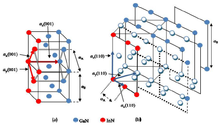
Figure 1 The direct zones of both bulk semiconductor and a (001) and (110) growth axis SL s , with one InN monolayer and with different numbers of GaN monolayers. The set of primitive translation vectors a x ; a y and a z of the SL s are also shown in this figure. a0 and a SL are the lattice constants of the bulk and the superlattice, respectively. a) (001) growth axis SL s and b) (110) growth axis SL s
Here, the value of a0 is a lattice constant of bulk materials, with L = (m
+ n)/2. The volume of the (001) and (110) SL
s
direct primitive unit cell is
3.Results and discussion
3.1.Structural properties
The Study of confinement effects and electronic structures in SL s (InN) m /(GaN)n along the (001) growth axes has been considerably focused over the past decade, but the most interesting feature is to know the effect of crystal orientations on their properties and their potential applications 34. There is a wide variety of the growth axes enabling the realization of the SL s . Two cases will be used: SL s grown along with the (001) and (110) directions. While the structural properties of (001)-oriented semiconductor SL s have been studied in great detail by using first-principles methods, there is not a comparable amount of information about the properties of (110)-oriented SL s 12. It is reported that (110) oriented SL s exhibit considerably different characteristics compared to those grown along the (001) direction. We theoretically calculated these variations on ideal cases and to verify the expectation that their properties represent. The calculations in this work are carried out on ideal cases in which all atoms of the bulks or SL s are located in ideal positions. By choosing the SL s which have a short period, we can assume that the lattice parameter is constant throughout the crystal as the distance between the successive interfaces is very small. This approximation liberates us from any calculation of relaxation. For the considered structures, we perform the structural optimization by minimizing the total energy with respect to the cell parameters and also the atomic positions.
For the binary compounds, the simplest structure is an eight-atom simple cubic
cell. For both directions (001) and (110)-oriented SL
s
, the smallest ordered structure is a four-atom tetragonal cell,
corresponding to the SL(1,1) and the largest ordered structure is a sixteen-atom
tetragonal cell, corresponding to the SL(1,7). The calculated total energies at
many different volumes around equilibrium were fitted by the Murnaghan equation
of state35 in order to obtain
the equilibrium lattice constant a0 and the bulk modulus B for the
binary compounds and all SL
s
. It should be noted that the period of our SL
s
is
Table I Calculated lattice parameter a0 and bulk modulus B for the binary compounds InN and GaN at equilibrium volume compared to the available theoretical and experimental data.
| Lattice constant a0(Å) | |||
| Present | Expt. | Theoretical studies | |
| InN | 4.940 | 4.98[36] | 4.947[8], 4.98[38], |
| 4.995[39], 5.05[40] | |||
| GaN | 4.480 | 4.50[43] | 4.556[44], 4.46[45], |
| 4.48 [46] | |||
| Bulk modulus B (GPa) | |||
| Present | Expt. | Theoretical studies | |
| InN | 141.23 | 137[41] | 140.76 [8], 146[42] |
| GaN | 192.564 | 190[47] | 190.932[48], 172.2[49] |
| 206.9[50] | |||
The lattice constant and bulk modulus for (InN)/(GaN)n for different values of n
in both directions (001) and (110)-oriented SL
s
were calculated and are listed in Table
II. As expected, the calculations for the (001) and (110) SL(1,1)
give the same results since the symmetry is the same. The link between the bulk
and the SL direct lattices is shown in the Fig.
1 with
Table II The structural parameters of superlattices (InN)/(GaN)
n
. Formation energies per atom are also listed. a0
represents the lattice constant and B the bulk modulus for the SL
s
. In the case of SL; a0 is shown in Fig. 1 and the link with the SL
lattice parameter is obvious:
| (001)-oriented Superlattice | |||||
| Compounds | a0(Å) | a0,SL | c0/a0 | B(GPa) | Eform (eV) |
| InN/GaN1 | 4.854 | 3.433 | 1.414 | 127.836 | -0.0074 |
| InN/GaN3 | 4.712 | 3.332 | 2.828 | 146.225 | -0.0072 |
| InN/GaN5 | 4.685 | 3.313 | 4.243 | 214.630 | -0.0057 |
| InN/GaN7 | 4.640 | 3.281 | 5.657 | 310.397 | -0.0048 |
| (110)-oriented Superlattice | |||||
| InN/GaN1 | - | - | - | - | - |
| InN/GaN3 | 4.728 | 3.343 | 1.414 | 146.666 | -0.0097 |
| InN/GaN5 | 4.658 | 3.294 | 1.414 | 210.661 | -0.0082 |
| InN/GaN7 | 4.651 | 3.289 | 1.414 | 306.866 | -0.0075 |
It is very clear from Table Ithat the bulk
modulus for the (InN)/(GaN)n in both directions SL
s
increases with the enhancement of the number of monolayer 𝑛, which
suggests the same increasing for the compressibility of each compound. These
compounds became harder when the number of monolayers n increase. It represents
bond strengthening or weakening effects induced by changing the composition. The
stability of (InN)/(GaN)n SL
s
is examined by calculating their formation energies. The formation energy
per atom
where Etot is the total energy of the (InN)/(GaN) n and the total energy of its constituent parts GaN and InN. From Table IIanalysis, it can be found that formation energy for these SL s have negative values and decrease by a small amount with the number of monolayers. The sign of the formation energy indicates that the present systems are energetically more stable with increasing n and imply that these SL s are exothermic and also can be synthesized experimentally. The (001) SL s have formation energy slightly less than the formation energy of (110) SL s .
3.2.Electronic structure and density of states
In this section, we turn our attention to study the electronic properties of the parents InN and GaN binary compounds and their SL s via calculating the energy band structure by using our calculated values of the lattice parameter. The results exhibit that cubic GaN and InN are a direct bandgap, where the valence band (VB) maximum and conduction band (CB) minimum are found at the Γ point. The results clearly exhibit that the present calculated bandgaps of 0 eV for InN and 1.916 eV for GaN are, on the whole, underestimated compared to the experimental values of 0.7 eV for InN 52 and 3.20 eV for GaN 53, but are in right agreement with other theoretical studies. The large difference in the calculated values of the band gaps as compared to the experimental values can be explained by the well-known fact that, in the electronic band structure calculations within DFT, GGA underestimates the energy gaps in semiconductors, but this will not alter the conclusions of the present work since they are not related to the quantitative estimation of gaps.
The calculated band gap energies of (InN)/(GaN)
n
in both (001) and (110) directions as a function of the thickness of the
monolayer GaN are investigated and plotted. As an example we show Fig. 2 the band structure of two limit
configurations (n = 1 and n = 7), where E
f
represents the Fermi level. From the results of the calculated bandgap
energies, we find that these materials have a direct bandgap, both valence band
maximum and conduction band minimum are lying at Γ point, which is of interest
for optoelectronic devices. The symmetry points in Fig. 2 refers to the tetragonal Brillouin zone (BZ) are (X, M Γ, Z,
A and R) in (001) direction case and those in (110) direction case are (X, M, Y,
Γ, Z, A, R and B). In the case of (001) SL(1,1) the high symmetry points B and Y
are identical to R and X, respectively. This remark remains valid for the (110)
SL(1,1), but B becomes different from R and Y from X when n increase. It is
noticeably indicated that the empty bandgap at the zone center is moved down for
these SL
s
for the bulk GaN band structure (not presented here). We also notice
significant changes in the CB ehavior near R, A, Y and Z for (110) compared with
(001). When n increase, the bottom of CB at R and A becomes higher, and it is at
Z for (001)- SL
s
and Y for (110) SL
s
that the bottom of CB starts to lower rapidly. This competition between
different high symmetry points of the SL
s
is mainly due to the zone folding effect, which is a typical feature for SL
s
. In other words, BZ of bulk binaries are folded into a smaller zone in a SL
s
. In fact, any wavefunction of the SL
s
at any high symmetry point kSL can be written as a linear combination of
the wavefunctions of the bulk constituent materials at specific points
kB of the bulk. These points are linked to each other by the
following formula:
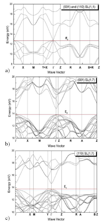
Figure 2 The band structure of superlattice (InN)/(GaN) n with n = 1; 7 for both (001) and (110) cases.
Table III The gap energies (in eV) between the upper VB and the lower CB.
| Gaps | Both (001) and (110) SL (1,1) | (001)-SL (1,3) | (001)-SL (1,5) | (001)-SL (1,7) | (001)-SL (1,3) | (110)-SL (1,5) | (110)-SL (1,7) |
| Γ-Γ | 0.0819 | 0.635 | 0.777 | 0.971 | 0.589 | 0.677 | 0.879 |
| Γ-X | 4.339 | 3.532 | 4.0631 | 3.936 | 3.229 | 3.912 | 3.207 |
| Γ-Y | Y does not exist in SL(1,1) | Like Γ-X | Like Γ-X | 4.464 | 2.877 | 2.227 | 1.864 |
| Γ-M | 3.116 | 3.261 | 3.308 | 3.298 | 4.568 | 3.222 | 3.610 |
| Γ-Z | 3.169 | 2.222 | 1.738 | 1.577 | 3.464 | 3.829 | 3.823 |
| Γ-R | 2.809 | 4.276 | 3.698 | 4.136 | 3.472 | 3.741 | 3.838 |
| Γ-B | B does not exist in SL(1,1) | Like Γ-R | Like Γ-R | Like Γ-R | 3.885 | 3.731 | 3.985 |
| Γ-A | 5.687 | 4.323 | 3.811 | 3.589 | 5.317 | 4.819 | 4.520 |
In order to estimate the effect of n number of monolayers into
(InN)/(GaN)n SL
s
on energies band gaps, we have plotted in Fig. 3 the variations of the Γ- Γ gap versus SL thickness in both
directions (i.e., versus the number n of monolayers). We remark that the Γ - Γ
gap increases with thickness from n = 1 to n = 7 by 0.889 eV and 0.797 eV for
the two directions (001) and (110) respectively. We also notice that the Γ - Γ
gap in (001) differs by more than 92 meV from the (110)-oriented SLs;
this can be understood by considering the orientation dependence of the ordering
potential in the (110) direction, which is given by
Such quantum confinement effects will influence the Γ - Γ bandgap values of these SL s . According to Ref. 57, the conventional InN/GaN QW are found to be type I, signification that the band gap values of SL s are controlled by the InN region, but the major challenges for this conventional system are the largely spontaneous and piezoelectric polarization fields, which significantly reduce the optical gain of the SL s . However, compared to the (001) case, the direction (110) is predicted to exhibit low quantum confinement effects, i.e., there is a low built-in electric field in the well InN or barrier GaN regions. We can conclude that for a rationally period and low concentrations of In, these conventional systems are very good optical materials.
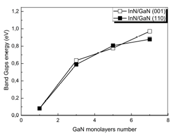
Figure 3 Direct band gap energies (Γ - Γ) as a function of the number n of monolayers in the superlattice (InN)/(GaN) n for both (001) and (110)-oriented SL s
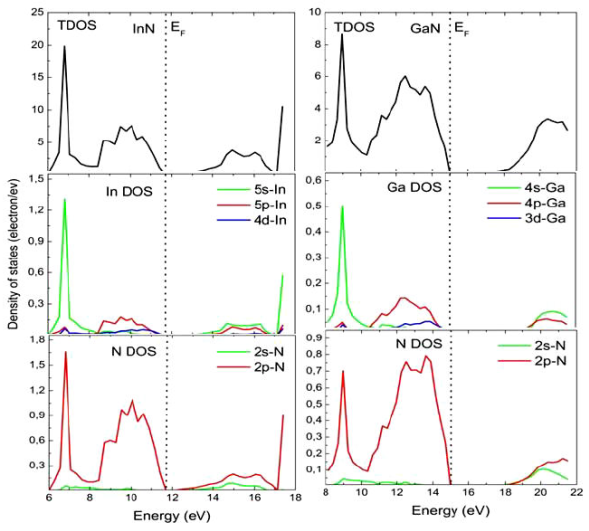
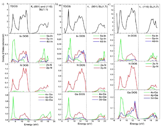
In the following, we want to comprise what happens in the two cases of SL s by comparing directly the peaks of the different density of states (DOS) curves and by analyzing the partial densities as a function differents numbers of GaN monolayers in the. For reasons of comparison, the DOS of the bulk materials have been calculated. The VB of binaries was divided into low, intermediate, and high-energy subbands. In both InN and GaN, we have found that VB near the Fermi level E f was mostly due to orbital p of In and N and orbital d of Ga and In atoms, while the greatest contribution to the bottom of CB was due to orbital p of N and s of In for InN and orbital s of N and Ga and orbital p of N for GaN (Fig. 4). As an example, we show in Fig. 5 the total and partial density of states of two limit configurations (n = 1 and n = 7). The total and partial DOS profiles illustrate the participation in the electronic interactions orbital and their positions. The first little peak, which occurs in the VB of (001) and (110) SL s , shows a strong contribution from the s orbital of Ga atom. The following VB peaks are all due to a high mixing of orbitals p of the three atoms N, Ga and In and orbital d of Ga and In atoms. The CB peaks are all due to a high mixing of p, s, and d orbital of N, Ga and In atoms for both (001) and (110)-oriented SL ´s. We can see a little difference in the (110)-𝑆 L8 , where the contribution of the orbitals 𝑑 of In atom and 𝑠 of N atom decrease (increase) considerably from n = 3 to n = 7 in VB near E f . It is clear from these results that the orbitals contribute almost similar to the higher VB’s and lower CB’s in the (001) and (110)-oriented SL s . The conclusion given in this section will be confirmed by the investigations of the optical properties reported below.
3.3.Optical Properties
It is fundamental to know to acquaint the optical activity of materials for their
application in optoelectronic devices. In this consideration, we investigate the
optical properties of both directions (001) and (110)-oriented SL
s
for different monolayers n. These important properties may be attracted
per the complex dielectric function
Where k is the extinction coefficient, λ is the wavelength of light in the
vacuum. To show all the possible optical transitions, we have increased the
number of special points in the First BZ up to 600 k-points, with an energy
range of up to 20 eV. Figure 6 shows the
real and imaginary parts of the dielectric function for SL(1,3), SL(1,5), and
SL(1,7) compounds for both growth axis. The occurrence of the peaks in
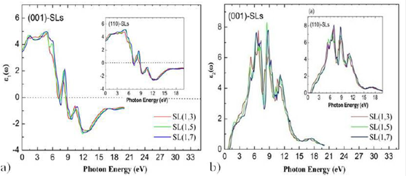
Figure 6 Calculated dielectric functions (real and imaginary parts) for (InN)/(GaN) n superlattices at direct band gap for the (001) ) growth axis direction. The inset of figure shows the real and imaginary parts plot for (110) ) growth axis direction.
This point represents the fractionation
The variation of the
The refractive index of (InN)/(GaN)n SL s is a valuable tool for the design of photovoltaic and optoelectronic devices. In order to study the transparency of SL s in response of an incident light the relation of Eq. (3) is used for computed the theoretical refractive index values for all SL s . The refraction spectra n(x) and refractive index n(0) are depicted in Fig. 7a and reported in Table IV. For the calculated SL s n(x) is not presenting a large variation for the photon energy in the near infrared or visible radiation. As a result , the static refractive indices n(0) are estimated from the refraction spectra (see Table IV).The maximum refractive index is reached for photon energy around 5.0, 4.89, 6.23 eV for (001) case (5.10, 5.40, 5.30 eV for (110) case), respectively. The spectral plots of the refractive index of Fig. 7a show an increasing from 2.424 (for n =3) to 2.449 (for n = 7) in the (001) SL s , and its value increases from 2.424 (for n = 3) to 2.457 (for n = 7) for (110)-oriented SL s . According to the result in both directions, the influence of the indium composition in the refractive index values of SL s are more important for (001) direction compared to the (110) direction, which allows us to say that the refractive index of SL s depends on growths axes.
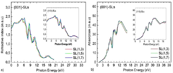
Figure 7 Calculated Refractive indices n(ω)(α) and absorption coefficients α ( ω)(b) for (InN)/(GaN)n superlattices for the (001) growth axis direction. The inset of figure shows the Refractive indices and absorption coefficients plot for (110) growth axis direction.
Table IV Calculated static optical constants ε1(0) and Static refractive index n(0) for (InN)/(GaN) n Superlattice compounds.
| (001)-oriented Superlattice | ||
| Compounds | ε1(0) | n(0) |
| SL(1,3) | 3.502 | 1.871 |
| SL(1,5) | 3.490 | 1.868 |
| SL(1,7) | 3.396 | 1.842 |
| (110)-oriented Superlattice | ||
| Compounds | ε1(0) | n(0) |
| SL(1,3) | 3.553 | 1.885 |
| SL(1,5) | 3.365 | 1.834 |
| SL(1,7) | 3.312 | 1.820 |
The optical absorption spectra are calculated in order to distinguish the optical nature in the SL s . The dispersion in the optical absorption spectra of the SL(1,n) grown along both directions (n = 3,5,7) are plotted in Fig. 7b. The absorption peak of both directions shifts to higher energy when n increases and the threshold energy increases. We observe from the curves of Fig. 7b that the absorption edge begins from the energy values of 0.600, 0.833, and 1.0 eV for (001) case (0.600, 0.766 and 0.9 eV for (110) case), respectively. It shifts towards lower energy when compared to bulk GaN, whose threshold is located at E s = 2.05 eV. Two major peaks at approximately 7 eV and 8.9 eV in the absorption coefficient for both growth axes represent the absorption of light at two different wavelengths. The maximum value of a(ω) is approximately 12.5 eV for (001) case (12.8 eV for (110) case) for all values of n, then the absorption coefficient abruptly decreases for the light photon above these energies. The intensity of absorption spectra diminishes with the inclusion of In contents in GaN layers.
As a result, the main conclusion to retain from all these curves is that the growth direction (110) does not ameliorate the optical activity. The similar contribution of the atomic orbitals to the electronic properties is probably the main reason for which the optical properties are expected not to be modified significantly. We suppose that the contribution of great cells will not change the present conclusions, on account of increasing the cell will only make the contribution of the bulk important compared to that of the interface and may not ameliorate the optical activity anymore.
4.Conclusion
To sum up we presented an ab-initio calculation on the electronic and optical features of short-period (InN)/(GaN) n superlattice systems, with n varying between 1 and 7, within both directions (001) and (110) using the FPLMTO+GGA96 method, which allows an accurate treatment of the interstitial regions. For the electronic proprieties, these (110) systems have a semiconductor behavior with variable energy gaps values. It is also observed that the band structure of all superlattices possesses a direct bandgap. Furthermore, the calculated dielectric functions, refractive index, and absorption spectra of the (001) SLs tend not to be quite different from those of (110) SLs. The reason is the slight differences between the contribution of the atomic orbitals to the electronic properties in both directions. The investigations were not extended to large systems because the contribution of the orbitals to electronic properties may reproduce, and the same conclusions should hold.

