


 nueva página del texto (beta)
 Inglés (pdf)
 Artículo en XML
 Referencias del artículo
 Enviar artículo por email
 Citado por SciELO
  Similares en
SciELO
Similares en
SciELO 
 Permalink
1. Introduction
Nowadays, precise DC and AC transducers for the continuous monitoring of electrical current is critical in our daily life. The correct measurement of this electrical quantity can determine the health state of one person and contribute to an accurate diagnosis, or possibly be related to conformity assessment activities of products in the automotive industry, aeronautics industry, steel industry, power generation, and in many other industries in general. Due to the increment of non-linear loads in the electrical network, there has been an increasing demand on high-precision current sensors, and its transducers for a wide variety of applications. Typical requirements for the sensors are a simple structure, wide bandwidth, reliability, low-Temperature Coefficient of Resistance (TCR), low self-heating, and robustness in sensing environment. In the case of transducers, is required a high precision interface insensitive to load and excellent stability from DC to kHz range [1-7].
Passive elements such as resistive current transducers have the main disadvantage that the electric circuit must be opened for introducing the measurement sensor. However, for harmonics and low-frequency disturbances under nonstationary conditions measurements, resistive current transducers are the best option over other current transducers such as Rogowski coils, Hall current sensors, classic current transformers, current comparators, magneto-optical current sensors, Superconducting Quantum Interference Device (SQUID) current sensors, and current clamps. Resistive elements avoid geometrical dependency errors, complex magnetic circuits, and complications associated with electronic instrumentation for compensated frequency dependence [8]. For the reasons explained above, in this work, an enhanced resistive current transducer is proposed. Its design provides high-precision, high-stability for continuous current monitoring, and excellent wideband. This device delivers two outputs voltages; a DC output voltage electrically isolated from its input, and other AC or DC voltage output that is taken directly from the passive element contacts.
Contemporary techniques such as thin-film technology and sputtering deposition techniques allow the design and fabrication of high precision resistors. The behavior of a precision thin-film resistor is determined not only by the purity and the resistivity of the material itself. The overall properties of the resistor are affected by the influence of its layout design, interconnection elements, environment, and substrate used, including its relevant properties in design conceptualization, i.e., flatness and polishing [9,10].
Nickel-Chromium (Ni-Cr) alloy is one of the most commonly used resistive materials for fabricating precision thinfilm resistors and up to highest-performance hybrid integrated circuits. This transition metal alloy exhibits different and useful properties depending upon the Ni-Cr composition and sputtering process parameters, making this alloy an excellent option for the electronics industry. Some of its most interesting features are low and adjustable TCR, high-stability of electrical properties, high thermal stability, excellent long-term reliability, low noise, low distortion, an approximately linear ratio between its electrical resistance and its thickness, corrosion resistance, chemical stability, and high melting temperature. Additionally, Ni-Cr alloy of 80:20 concentration percent of each element in weight (wt-%) is considered optimal for the fabrication of thin-film precision resistors [11-16]. For the reasons mentioned above, a Ni-Cr alloy with a concentration of 80:20 wt-% was selected for this work.
For continuous current monitoring, the self-heating and the temperature rise of the resistive current transducer due to Joule heating are controlled by design. A custom heatsink for this application was sized to allow continued use of the resistive current transducer. Aluminum Nitride (AlN) is a new generation of ceramic material whose main characteristics are high electrical resistivity and high thermal conductivity. Its outstanding heat dissipation is an essential characteristic in the high-power electronics industry where hightemperatures are inherent [17-22].
This section exposed the motivations for the present proposal on the design of a high-precision current transducer and the reasons for choosing the selected materials for its manufacture. Section 2 presents the design principles used in the resistive current transducer aimed at providing a high accuracy input-output ratio with a linear response through all its bandwidth. Section 3 provides all the simulation analysis of the resistive current transducer to prove its performance under different test conditions, including its behavior before highly distorted current signals. Finally, Sec. 4 presents the conclusions of this work.
2. Resistive Current Transducer Module Design Process
2.1. General Description
In this paper, the Resistive Current Transducer (RCT) was designed for the continuous monitoring of DC or AC. A maximum nominal current of 1.25 A can flow through all its elements without any damage. For the optimal handling of the dissipated heat, four modules with similar electrical and thermal characteristics form the RCT in a highly symmetrical configuration. Therefore, efficient thermal energy management was implemented based on an AlN heat sink to avoid the thermal drift of the resistance value of the RCT and its aging due to thermal shocks. The RCT provides two voltage outputs, a not electrically insulated voltage, which is taken directly from the resistive elements, and an electrically insulated voltage based on a thermopile. The housing of the RCT provides an adiabatic environment that minimizes heat exchange with the surrounding during the thermal time constant of the system, time in which the thermopile transforms the temperature difference into a thermoelectric electromotive force by the Seebeck effect completely. The maximum voltages at full-scale for the not electrically insulated output and the electrically insulated output are 0.25 V and 0.037 V, respectively.
In the case of AC, its negligible frequency dependence is based on the design of a coaxial and highly symmetric circuit of the electric current to be measured, to reduce the self-inductance of the sensor, and minimize capacitive leakage currents. These design criteria allow the RCT to deliver an accurate, not electrically insulated output voltage signal for input current waveforms with low-frequency disturbances under non-stationary conditions, high-frequency current waveform, or high-distorted current waveforms because of its harmonic content.
2.2. Mechanical and Electrical Assembly of the RCT in its Housing
The housing provides a stable thermal environment for the operation of the RCT, in which the temperature changes on the outside are attenuated in such a way that they do not affect the temperature inside during the AC or DC measurement. Therefore, in this design, the heat transfer process is expected to be the same for periods greater than the thermal constant of the system. Thus the comparison between the Joule heat produced by DC and the Joule heat produced by AC will be carried out under the same thermal equilibrium conditions by the thermopile. For the user, the housing presents the mechanical means of connection for the electrical input and output signals. The connection of the input current is made through an N-type connector, model 082-97-RFX [23], which is correctly sized to support a current greater than 1 A. A LEMO connector, model EGG.0B.304.CLL, which is fully shielded to prevent electromagnetic interference, was selected to access the output voltage signals from the RCT [24]. Figures 1a) and 1b) show the housing and connectors of the RCT described above. The input current connector is located on the top cover of the housing, and the output voltage connector is located on the side. The outer and inner diameters of the housing are 120 mm and 100 mm respectively, with a height of 100 mm without including the height of the input current connector. A C2800 brass alloy was selected for its manufacture, which is composed basically of Copper and Zinc in a 60:40 concentration percent of each element in weight. The main characteristics of the alloy used for this housing are: excellent machinability and ductility, high resistance to oxidation and corrosion, resistance to wear, high electrical conductivity, and its capability to support high temperatures [25].
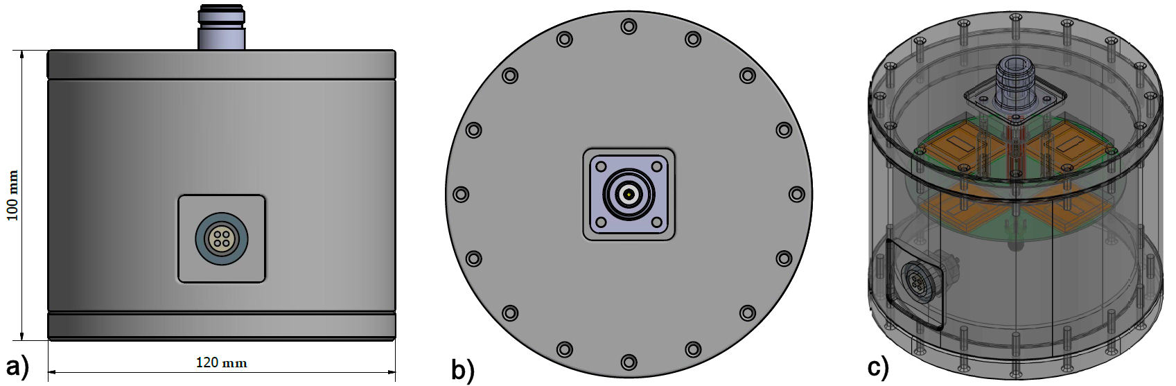
FIGURE 1 Housing assembly and geometric distribution of external and internal components of the resistive current transducer. a)Front view. b)Top view. c)Isometric internal view.
Inside the housing, a Printed Circuit Board (PCB) is mechanically and electrically coupled to its upper cover. The input current path is defined from the central pin in the current input connector to the PCB, consisting of four rounded copper wires. The output current path is defined from the PCB to the upper housing cover, and it is made by four hexagonal copper pillars. The PCB has a coaxial and highly symmetrical design, which is responsible for the division, distribution, and return of the current between the input current connector and each module that forms the RCT. Figure 1 shows the housing, the mechanical and electrical coupling previously described, and the geometric distribution of the internal components of the RCT.
The mechanical design of the housing allows prompt assembly for the user. The main components of the RCT are available after removing the bottom housing cover. Figure 2 shows the assembly order of the RCT, beginning from step (a) to step (h). The body, the output voltage connector, and the bottom cover of the housing are not shown.
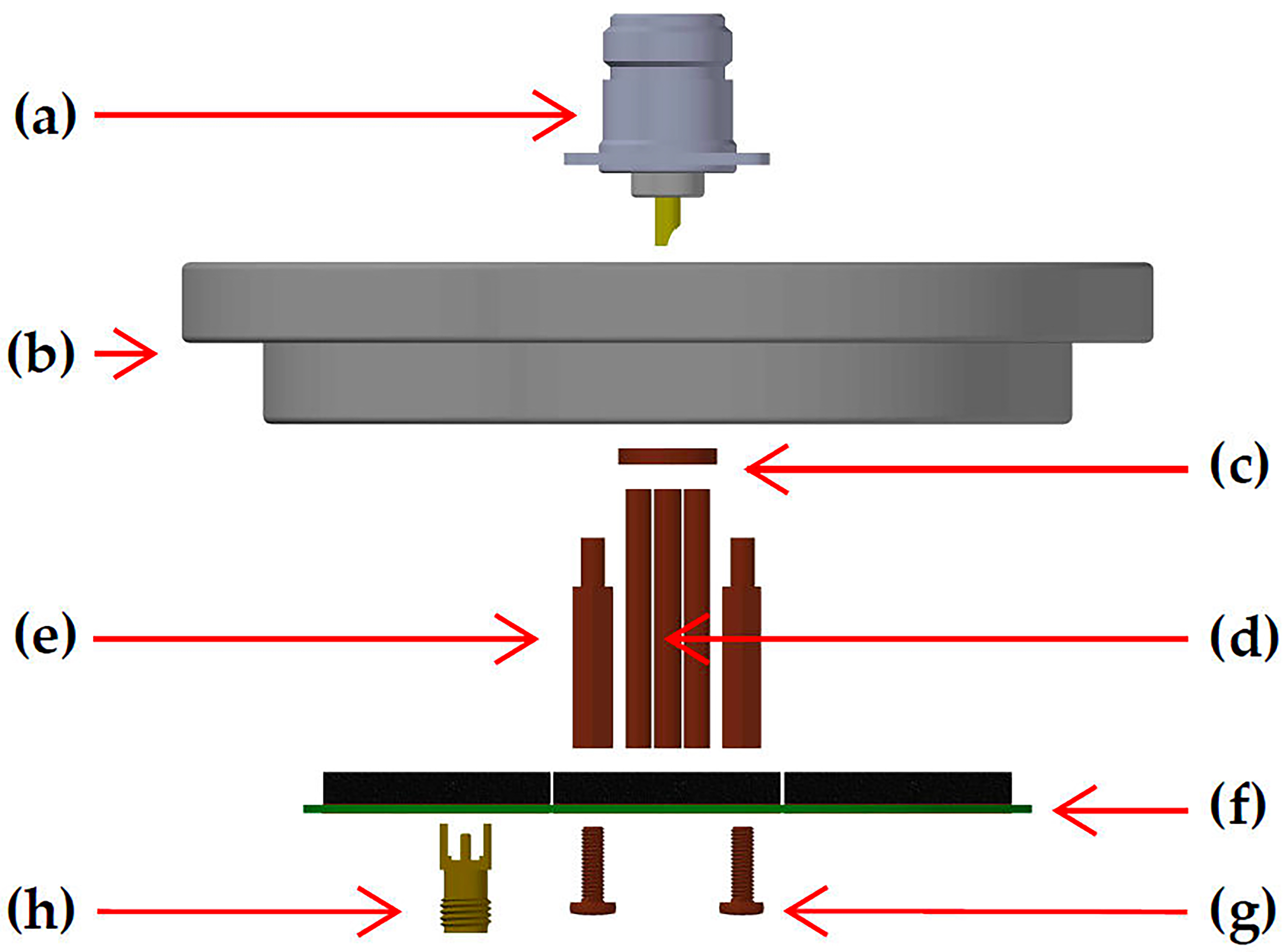
FIGURE 2 Order in which the mechanical assembly has been performed: (a) Current input connector. (b) Upper housing cover. (c) Copper wires aligner. (d) Round Copper wires. (e) Hexagonal Copper pillars. (f) PCB with the RCT modules. (g) M3 x 10 mm Copper screws. (h) SMA 50 Ω connectors [26] are optional, to connect the output voltages from the PCB to the LEMO connector. Direct wiring from the PCB to the LEMO connector is also possible.
2.3. Thin-Film Resistance Manufacturing Process at Centro Nacional de Metrología
The RCT is formed by four modules. Each module consists of a heat sink and a thin-film resistor. The four modules are connected in parallel; thus, only a quarter of the input current is going to flow through each thin-film resistor. The thin-film resistors were deposited by the sputtering technique [27]. A commercial target of Ni-Cr alloy in 80:20 wt-% concentration, with a diameter of 76.2 mm and a thickness of 3.175 mm, was used for their growth [28]. An AlN ceramic substrate was chosen for its high thermal conductivity suitable for high power dissipation applications it acts as a heat sink with custom-sized to operate continuously at a current of 0.25 A. It is known that Ni-Cr alloys have adequate properties for use with AlN substrates because of its excellent adhesion to it [29]. A fully automatic sputtering system was used for the thin-film resistor deposition.
A set of four Ni-Cr thin-film resistors were manufactured during the same deposition process. By maintaining the same deposit characteristics such as Ni-Cr target, chamber pressure, Argon gas input flow, deposition rate, substrate rotation speed, a substrate to target distance, and polarization voltage, the homogeneity of the thin film resistors electrical characteristics is increased. The resistors have a nominal resistance of 1 Ω. For the growth of the resistors, a base pressure of ∼ 10−7 Torr was achieved in the chamber; the Ar flow during growth produced a working pressure of ∼ 10−3 Torr. Before deposition, a pre-sputtering procedure was carried out to clean the target surface for 10 minutes. The system was programmed to obtain a thickness of 1.1 microns with a deposition rate of 1 Å·s−1. The substrate was not heated intentionally. Its rotation was set to 20 revolutions per minute. The films remained in the sputtering vacuum chamber until the next day to allow them a slow cooling and thus preventing them from thermal shock and fracturing.
Thin-films with a thickness of 1.1 µm and different geometries were manufactured in independent processes onto glass substrates to characterize thickness reproducibility. A profilometer KLA-Tencor model D-120 was used to measure the thickness of the thin-films (step-height measurement). Before each set of measurements, the profilometer was calibrated against a step height standard, which has a nominal value of 1 µm with a calibration uncertainty of 0.025 µm for a coverage factor of k = 2.0. This characterization process shows that it is possible to achieve reproducibility of ±0.1 µm for thicknesses of 1.1 µm. Figure 3 shows some of the films deposited with different geometries and thicknesses.

The thin-film resistance nominal value can be calculated from Eq. (1):
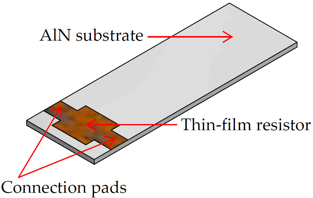
where ρ is the Ni-Cr resistivity, l is the length, w is the width, and t is the thickness of the film. Substituting ρ = 1.1 Ω/m, l = 2 mm, w = 2 mm, and t = 1.1 µm, the thin-film resistance is 1 Ω. Figure 4 shows the resistor onto the AlN substrate. The connection pads are not taken into account for the calculation of the resistance presented above.
2.4. Heat Sink for Continuous Current Monitoring
For this design, the substrate where the thin-film is deposited also serves as a custom-designed heat sink, and it is responsible for transporting the heat generated by the Joule effect out of the thin-film resistor. AlN belongs to a new generation of ceramic materials with high thermal conductivity and high electric insulation; it is widely used in power electronics to increase current-carrying capability and manage the generated heat. The crystalline quality and the effective thermal conductivity of the films are found to be improved with the increase of film thickness. Table I shows the relation of its thermal conductivity concerning its crystalline quality and film thickness [17]. Because of this characteristic, after determining the substrate dimensions, it was ordered from a specialized manufacturer [30].
TABLE I Thermal conductivity of AlN with different crystalline quality.
| Thickness (µm) | Thermal conductivity (W·m-1·K-1) |
| 1 | 7.5 |
| 5 | 9.8 |
| 10 | 13.3 |
The time constant τ of the system is finite and shows the relationship between the heat dissipated in the resistor, and the size of the heat sink. The time constant τ is proposed by design to be 1 s, and it allows the correct integration of lowfrequency signals, as it will be shown later in the paper. To determine the size of the AlN heat sink, the following procedure was followed. Equation (2) shows the ratio between the heat capacity of the heated area C and the heat conductance between the heat generator and the heat sink K Th [31].
The power P generated by the thin-film resistor and the current flowing through it is calculated as P = I 2 ·R. In this case, P = 62.5 mW with R = 1 Ω and I = 0.25 A. The heat conductance K Th showed in Eq. (3) expresses the ratio between the generated power P, and the expected temperature rises ∆T = 3 K, proposed by design [32].
With τ = 1 s, and K Th = 20.83 mW·K−1, the heat capacity obtained is C = 20.83 mJ·K−1. The technical specifications of the commercial AlN AN-230 substrate are presented in Table II. For continuous operation, the target volume V AlN is obtained from Eq. (4).
TABLE II MARUWA AlN substrate characteristic values [30].
| Thermal conductivity | k | 230 | (W·m−1·K−1) |
| Specific heat | Cp | 720 | (J·kg−1·K−1) |
| Density | p | 3 250 | (kg·m−3) |
The computed target volume V AlN = 11.98 · 10−9 mm, translates into a thickness of 0.25 mm, a width of 4 mm, and a length of 12 mm. Figure 5 shows the custom-sized substrate for this application. A critical feature of this substrate is its polishing, which has an average roughness of 0.05 µm. Although this polishing significantly increases its price, this characteristic guarantees an excellent adhesion onto it for a thin-film with a thickness of 1.1 µm.

To obtain information about the heat transfer process on the AlN substrate, an abstraction to a fundamental solution, known as heat kernel, was used. Equation (5) shows the heattransfer equation for one-dimensional system [33].
where α is a real, positive constant known as the diffusion constant, and its value is obtained from Eq. (6) [33].
For specific initial conditions, when a heat-impulse is applied at the point x = 0 and at time t = 0, the solution to Eq. (5) is given by a Gauss distribution function shown in Eq. (7) [33].
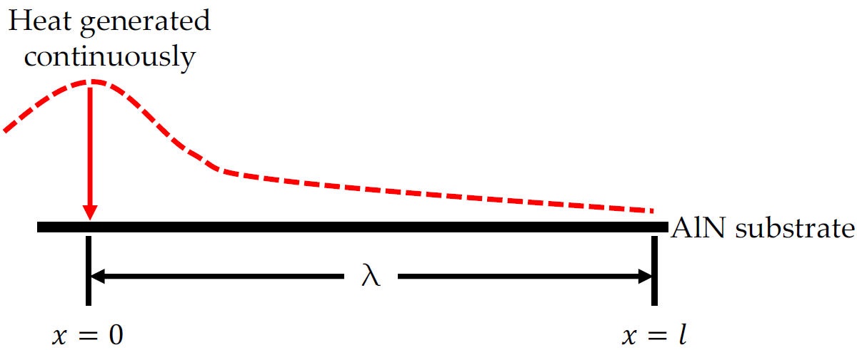
The width λ is a measure of the spread of heat during the time interval t, and it is computed from Eq. (8) [33]. When the heat is generated continuously, the temperature distribution conserves its shape with time. This means that as t → ∞ this fundamental solution becomes flatter, with its value at any x approaching zero exponentially.
The heat transfer distance λ = 20 mm, is computed with α = 98 · 10−6 m·s−1, and t = 1 s as previously proposed by design. However, as the Gaussian distribution is centered at the heat generation source, the effective heat transfer distance is half the value of λ = 10 mm. Figure 6 exemplifies the concept of heat transfer distance resulting from the heat source. The parameter α is closely related to the design of the DC output voltage electrically insulated. This is discussed in the following section.
2.5. DC Output Voltage Electrically Insulated
An electrically insulated DC output voltage is provided using the heat generated by the Joule effect, which is propagated and stored in the AlN substrate. This insulated voltage output signal can be used as a ratio measure between the input current and the non-insulated output voltage when the device is operated at a full scale. Besides it can provide information about the working condition of the RCT. For this purpose, a thermopile, which is a passive device composed of several thermocouples connected in series, is placed underneath the AlN substrate. The Seebeck effect, which is the increase of an electromotive force in a thermocouple, is generated through a dipole, consisting of two conductors that form two junctions maintained at different temperatures, under zero electric current [34]. The thermoelectric potential difference is often known as the Seebeck potential, in honor of the man to whom the discovery is attributed. The Seebeck potential between the terminals is going to depend on the temperature difference at the ends of the thermocouple or the thermopile, but not on the shape or dimensions of the conductors themselves [35]. Figure 7 shows the concept of a thermocouple composed of two dissimilar metals, and how several thermocouples connected in series forming a thermopile.
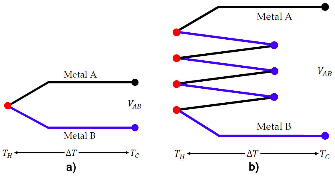
For a thermocouple and a thermopile, as shown in Fig. 7, the output voltage is given by Eqs. (9) and (10), respectively.
where the parameters α A and α B are the Seebeck coefficients of the metal A and the metal B, respectively. The algebraic physical quantity α AB is called the relative Seebeck coefficient, n is the number of thermocouples connected in series forming the thermopile, T H is the temperature at the hot junction, T C is the temperature at the cold junction, and ∆T is the temperature difference between T H and T C . For a small temperature difference, the Seebeck electromotive force can be assumed to be directly proportional to the temperature difference [36]. In the design presented in this work, as previously proposed in the Sec. 2.4, the expected temperature rise in the AlN substrate over the surrounding environment is 3 K. Therefore, a linear relationship between the output voltage and the temperature difference present at the thermopile junctions is assumed.
In general, applications involving thermoelectric devices need materials with high Seebeck coefficients, low thermal conductivity, and high resistivity. Semimetals possessing the properties mentioned previously are Antimony (Sb) and Bismuth (Bi). Particularly under the condition of high purity, Sb has a positive Seebeck coefficient, and Bi has a negative Seebeck coefficient [37].
To manufacture the thermopile, the thin-film deposition process was used twice, first for one semimetal, and then for the other. For this purpose, an Sb [38] and Bi [39] commercial sputtering targets were acquired with a purity of 99.999%. Each thermopile contains 25 thermocouples and has the following dimensions: a length of 8.2 mm width of 18 mm, and a thickness of 2 µm. Figure 8 shows the detailed design of the thermopile and how both semimetals have electrical contact at the ends. The hot junctions are defined at the center of the thermopile, and the cold junctions at the ends. It is important to note that the thermopile length respects the heat transfer distance λ previously computed, intending to provide a temperature as homogeneous as possible in the hot junctions of the thermopile.
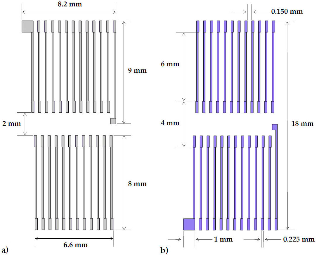
FIGURE 8 Bismuth-Antimony thin-film thermopile. a)Semimetal A: Antimony (Sb). b)Semimetal B: Bismuth (Bi).
A finite element simulation in Comsol Multiphysics for the coupled thermal and electrical fields was made to the thermopile design. Equation (13), is the governing equation that describes the interaction between the thermal and electric systems under the steady-state condition, and for homogeneous and isotropic materials [35].
where the first term ∇ · (k · ∇T) corresponds to the thermal conduction, the second term ρ · I 2 is the Joule heating, and the third term describes the thermoelectric effects.
The thermoelectric simulation used a 2D geometric domain which is justified by the thickness of the thermopile, and it is expected that the temperature distribution and the electrical potential are parallel to the width of its geometry. In this study, the temperature at the hot junctions T H is set to 299.15 K, and the temperature at the cold junctions T C to 296.15 K. Adiabatic conditions were assumed in the rest of the elements of geometry. Given that ∆T = 3 K, the convection and radiation losses may be considered negligible. Table III [36,40] shows the physical properties for Sb and Bi used in the simulation.
TABLE III Physical properties for the semimetals Antimony and Bismuth used in the simulation.
| Physical property | Symbol | Antimony | Bismuth | Units |
| Thermal conductivity | k | 24.3 | 7.87 | (W·m−1·K−1) |
| Specific heat | Cp | 207 | 122 | (J·kg−1·K−1) |
| Density | p | 6 680 | 9 790 | (kg·m−3) |
| Seebeck coefficient | α | +48.9 | -73.4 | (µV·K−1) |
| Electrical resistivity | ρ | 0.39 | 1.07 | (µΩ·m−1) |
Figure 9 shows the results obtained from the thermoelectric simulation for one thermopile; Although the finite element simulation of the four thermopiles, one thermopile beneath each AlN substrate, does not pose any significant difficulties under the simulation conditions stated previously, for the reduction of time and computational effort just one thermopile was simulated. This reasoning is justified because of the fabrication process, where the four thermopiles are manufactured during the same deposition process, the high purity of materials, the reproducibility of the sputtering system, and the high symmetry used in this design. The spatial distribution of the electric potential shown in Fig. 9a) depicts the potential drop between the positive (in red color) and the negative (in blue color) terminals. The maximum output voltage is 9.17 mV for one thermopile, in the case of the four thermopiles connected in series, the maximum expected output voltage is 36.68 mV. Using Eq. (10) to compute the maximum expected output voltage from the four thermopiles connected in series, with n = 100, α AB = 122.3 µV·K−1, and ∆T = 3 K, the result obtained is 36.69 mV, which shows concordance with the results obtained from the simulation. The temperature distribution along the thermopile arms is shown in Fig. 9b). For this design, the thermopile length of the arm was bounded to define a homogeneous temperature gradient between the hot and cold junctions. The heat transfer distances for the Sb and the Bi are 4.2 mm and 2.6 mm, respectively. These reported values were calculated with Eq. (8) for a t = 1 s, and the physical properties presented in Table III. Finally, note that the temperature distribution length obtained from the simulation corresponds with the heat transfer distance of the material with the highest thermal conductivity.
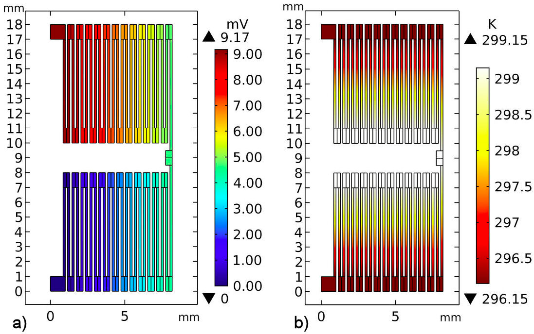
FIGURE 9 Thermopile thermoelectric simulation results. a)Thermopile output voltage. b)Thermopile temperature distribution.
The thermopile output voltage concerning the temperature generated by the input current is presented in Table IV . Note that the relation between the temperature rise and the input current is not linear. The reason is that the thermopile is thermally coupled to two heat reservoirs, one for the hot junction and one for the cold junction. The function of these heat reservoirs is to provide higher stability to the temperature to which the thermopile junctions are exposed, and they were sized to work with a nominal input current of 1 A.
2.6. Electrical Model
The electrical diagram presented in Fig. 10 considers the parallel connection of the four modules that form the RCT through which the input current I IN might flow. In this case, C 1 is the capacitance of the input current connector, R 1 and L 1 are the resistance and the inductance of the round copper wires, R 2 and L 2 are the resistance and the inductance of the hexagonal Copper pillars, C 2 is the capacitance between the previous elements; R 3, L 3, R 4, and L 4 are the resistance and inductance of the PCB top and bottom layers, C 3 and G 1 are the capacitance and conductance of the top and bottom layer in the PCB, R 5, L 5, R 6, and L 6 are the resistance and inductance of the connection wires from the PCB to the thinfilm resistor, C 4 is the capacitance between the connection wires described before, R 7, L 7, G 2, and C 5 are the resistance, the inductance, the conductance and the capacitance of the thin-film resistor. At the end of the electrical diagram, the output voltage V OUT is measured directly on the thin-film resistor R 7. It is important to mention that C 5 includes the capacitance of the output voltage connector. Additionally, the electric model allows identifying which elements have the most significant impact on the design, becoming it into a non-coaxial design. Therefore, the design seeks to be more specific in those elements. For example, capacitances and conductances in parallel affect the principle of coaxiality, since the input current does not return equally in the upper circuit layer (R 1 − L 1, R 3 − L 3, and R 5 − L 5) compared to the lower circuit layer (R 2 − L 2, R 4 − L 4, and R 6 − L 6). Thus, the coaxial design aims to ensure that these couples are equal in amplitude and phase.
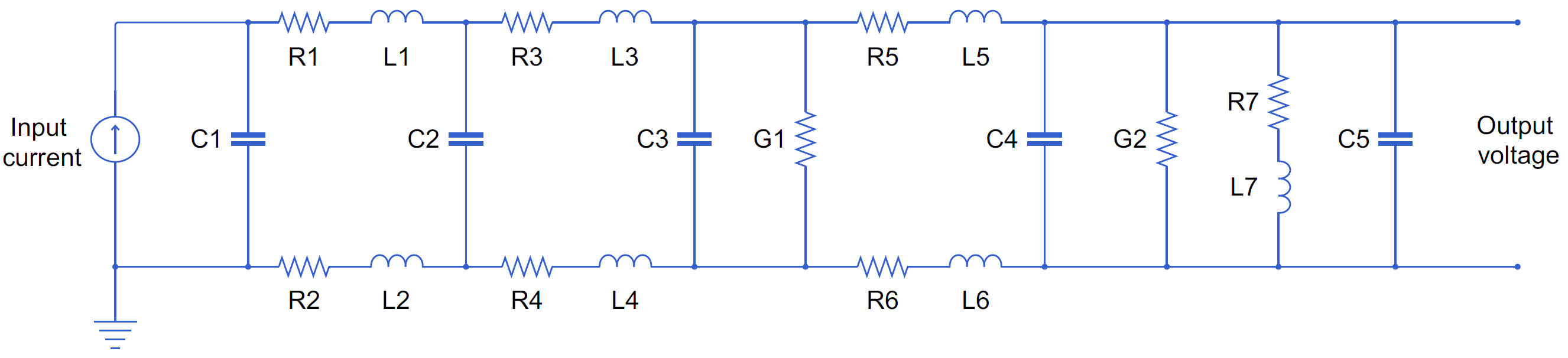
An analytical reduction was made to the electrical diagram presented previously in Fig. 10 to obtain information about the performance of the RCT regarding the frequency. The lumped block diagram is presented in Fig. 11, which allows to exemplify how the Transfer Function (TF) between the input current I IN and the output voltage V OUT was obtained.
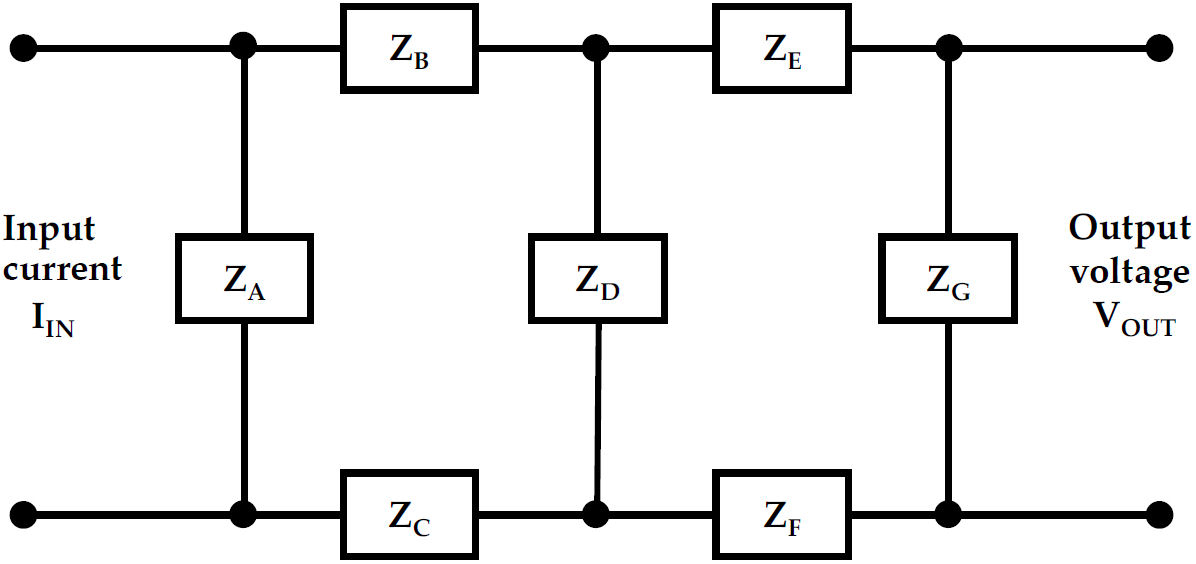
Equation (14) shows the TF between the output voltage and the input current, Eq. (15) contains the information of the Z G block where the thin-film resistor is connected in parallel to C 4, C 5, and G 2. During the reduction process, the Z G block was not combined with other blocks to avoid losing the terminals where the voltage measurement is defined.
An analysis of sensitivity was performed to identify the most critical components in the electrical diagram of the RCT. As a result of this analysis, R 7 and L 7 were identified as the most critical components, which makes sense because the voltage measurement is defined between their terminals. An iterative process was done for optimizing and linearizing the frequency response of the RCT. During this process, the effect of each of the non-critical components over R 7 and L 7 were evaluated. Factors such as geometry, the distance among components, thicknesses, and dimensions were taken into account to minimize and compensate the frequency effects over the RCT.
Figure 12 shows the magnitude and phase responses of the RCT in the frequency range from DC to 100 kHz. In this case, the magnitude was expressed as the relative error between the TF and the nominal resistive of the RCT. Note that at frequencies below 10 kHz, the denominator of the TF dominates and prevents the impedance of the RCT from increasing as the frequency does. At frequencies higher than 10 kHz, the numerator of the TF dominates, and the impedance of the RCT rises at the rate of 0.3 pΩ·Hz−1. Concerning the behavior of the phase angle of the RCT, it becomes noticeable at the frequency of 20 kHz, where it has a value of 0.6 m◦. For frequencies higher than 20 kHz the phase angle of the RCT rises at the rate of 31 n◦·Hz−1. In general, for monitoring current signals at line frequency and distorted waveforms a linear wideband of 10 kHz is recommended for magnitude and phase, which is covered by the RCT design presented in this work.

3. Simulation Analysis and Results
After the refinement and optimizing process on the design phase presented in Sec. 2, computer-aided simulation tools were used to analyze the thermal behavior, and the frequency response of the RCT, as described in the next subsections.
3.1. Thermal Behavior
Special attention was taken to the heat transfer phenomena that occur within the RCT enclosure, such as the heat transfer losses by conduction through the thermopile and the connection wires on the thin-film, heat transfer losses by convection, and heat transfer losses by radiation. Equation (16), presents the heat equation, which describes this three-dimensional thermal model.
The first term on the left-hand side of Eq. (16) represents the conduction heat loss between the heat sink, the thermopile arms, and the connection wires, and the second term is the heat generation due to the Joule effect. On the righthand side, the thermal diffusivity is defined and relates the thermal conductivity to the heat capacity of the material. The surfaces of the RCT enclosure are at room temperature T Room of 296.15 K, and the boundary conditions in Cartesian coordinates for all these surfaces on X, Y, and Z directions are: T(x,y,z,t) = T Room|x=0,X, T(x,y,z,t) = T Room|y=0,Y , and T(x,y,z,t) = T Room| z=0,Z , respectively.
The convection heat loss between the heat generator and the fluid is expressed by the Eq. (17). Where h is the coefficient of heat transfer between the solid surface and the fluid, A C is the surface area, and ∆T is the temperature difference between the solid surface of the heat generator and the surrounding room temperature.
The heat convection loss is not present in Eq. (16) because the heat transfer to the fluid inside the RCT enclosure is a special case of heat transfer in restricted spaces. The heat transfer in horizontal enclosed spaces involves, in this case, that the lower plate has a higher temperature than the upper plate so that no convective heat transfer can be expected in the enclosure of the RCT. Consequently, heat is transferred in the fluid (air) only by conduction of heat [41].
A two-dimensional study was done with the help of Comsol Multiphysics, aimed at showing the interaction between the heat generator and the air inside of the RCT enclosure. The distance from the floor to the ceiling inside the RCT enclosure is d = 2.9 mm. The physical properties of the fluid were taken from the software database. The isothermal contours and the temperature distribution of the fluid are presented in Fig. 13. In both cases, isothermal planes are formed instead of convection currents as expected. The heat loss transferred to the fluid by conduction is assumed to follow the cooling law of Newton, and it has a value of 4 µW, which is negligible compared to the input power of 62.5 mW, which represents less than 0.01 %.
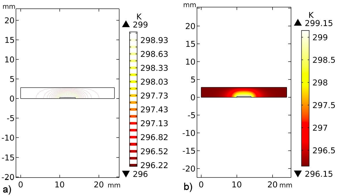
FIGURE 13 Heat losses by conduction in the air inside the RCT enclosure. a)Isothermal contours. b)Temperature distribution.
Thermal radiation is the electromagnetic radiation emitted by a body as a result of its temperature. When the energy density is integrated over all wavelengths, the total energy emitted is proportional to absolute temperature to the fourth power. The amount of energy emitted from the hot surface of the thin-film is assumed to follow the Stefan-Boltzmann law [41], shown in Eq. (18), where A R is the surface area of the body, and σ SB is the Stefan-Boltzmann constant which has the value of 5.670 · 10−8 W·m−2·K−4 [42].
A blackbody is considered one that absorbs all radiation incident upon it. For the current research, it has been assumed that the RCT enclosure is an entirely black enclosure so that all the radiation is going to be absorbed. At the same time, the enclosure will emit radiation following the T 4 law. Real materials emit less radiation than ideal black surfaces. Due to this fact, the concept of a gray body is defined trough a factor called emissivity ((, which is the ratio of the emissive power of the body to the emissive power of a blackbody at the same wavelength and temperature. Finally, to complete the radiation heat loss study, it is well known that not all the radiation leaving one surface is going to reach the other surface since electromagnetic radiation travels in straight lines and some of it is going to be lost to the surroundings. Thus, to quantify the amount of energy that leaves one surface and reaches the other, the radiation shape factor R SF is used. Equation (19) presents the radiation heat loss, considering the emissivity and the radiation shape factor for two parallel plates that are separated a distance d [41].
The convection heat loss has a value of 111 µW, and was computed with R SF = 0.16, A 1 = 48 µm2, A 2 = 576 µm2, (1 = 0.8, and (2 = 0.9 for the AlN block and for the RCT enclosure, respectively. This convection heat loss represents 0.2 % to the input power. For this reason, it is not considered in Eq. (16), as it was done with the convection heat loss term.
The conduction heat loss is the most significant transfer mechanism due to the thermal contact between the heat generator and heat conveyors such as the heat sink, the thermopile, and the connection wires that carry the input current inside the enclosure of the RCT. The total conduction heat loss was quantified as the linear combination of each thermal conveyor, and it is expressed by Eq. (20).
The first term on the right-hand side of Eq. (20) represents the heat sink (hs), the second term groups the thermopile legs Bi − Sb with n Bi−Sb = 25, and the third term is for the connection wires w with n w = 2, where for each element k is the thermal conductivity, A is the contact area, ∆T is the temperature difference, and l is the length. A threedimensional thermal study was done in Comsol Multiphysics aimed at minimizing the conduction heat losses due to the thermopile and the connection wires. Figure 1c) shows the geometry of the RCT for this study. The TF presented in Eq. (14) describes the frequency response of the RCT and in conjunction with the thermal study an iterative process was employed to find the best performance in both scenarios. As a result of these studies, the conduction heat losses for each element were quantized and minimized [43,44]. Their contribution concerning the input power is presented in Table V.
TABLE V Conduction heat loss for each element and its inputoutput power ratio.
| Conduction heat loss |
Heat loss (mW) |
Power ratio (%) |
| Qhs | 0.8 | 1.2 |
| QBi-Sb | 0.1 | 0.2 |
| Qw | 2.2 | 3.5 |
| TotalQConduction | 3.1 | 4.9 |
As expected, the connection wires represent the highest heat loss because they are the thermal anchor of the system, and their design allows a moderate heat flow to the housing of the RCT. These Nichrome wires have a length of 8 mm, and a radius of 0.3 mm. The stationary solution in Fig. 14 presents the behavior of the thermal and electrical model when a current of 1 A flows through the RCT. The isothermal contours and the temperature distribution allow observing the equilibrium heat flow for continuous operation. The maximum temperature rise is 299.6 K, as was selected by design from the beginning. The output voltage was computed by the software with the input current of 1 A, and the four thin-film resistors of 1 Ω connected in parallel.
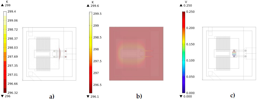
FIGURE 14 Thermal and electrical behavior of the RCT for input current of 1 A. a)Isothermal contours. b)Temperature distribution. c)Electrical potential.
The heat transfer distance and its shape in the heat sink are shown in Fig. 15. The optimal heat transfer distance λ was computed previously through Eq. (8). This parameter restricts the spatial location space of the thermopile under the heat sink, and it has a value of 10 mm. The dotted vertical lines represent the spatial location of the thermopile; it is within the distance mentioned above, defined from the heat source. The heat sink acts as a heat reservoir for the thermopile hot junction, maintained at a temperature of (299.4±0.1) K. In the case of the thermopile cold junction, it is maintained at a temperature of (296.3±0.2) K. Thus, the temperature difference between the hot and cold junction of the thermopile has a value of ∆T = 3.1 K and provides an output voltage of 37.9 mV.
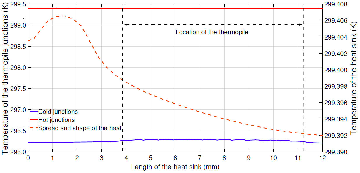
FIGURE 15 Heat-impulse in the AlN block, the location of the thermopile (dotted vertical lines), and the temperature profiles at its junctions generated by the input current of 1 A.
A time-dependent study was done to know the heat propagation and the temperature value associated with specific working time in the system. The time proposed by design to reach a temperature rise of 3 K in the heat sink over the surrounding environment is 1 s. In this analysis, the room temperature was set to 296.15 K, and the input current to 1 A. Figures 16a) to 16e) present the time-dependent results from the initial-state to the steady-state condition. Note that the target temperature is reached at a time of 1.5 s instead of 1 s. The reason is that the thermal mass of the AlN block has been increased due to the thermal contact with the thermopile hot junction underneath, and the current wires on its top. Finally, it can be observed that for a time of 1.5 s, the AlN block has reached the target temperature, and it has practically the same temperature at its steady-state condition, Fig. 16e).

3.2. Frequency Response
A frequency response analysis of the RCT was performed by applying input current signals of different characteristics to its TF. Accordingly, the output voltage V OUT may be obtained through the following expression.
The frequency dependence and linearity of the current transducers are the most critical factors that may decrease its accuracy. The TF of the RCT provided information about the performance of its impedance concerning frequency. Derived from that analysis, it may be assumed a negligible impact to its accuracy due to these parameters. The linearity ratio between the input current I IN and the output voltage V OUT was evaluated with current signals of amplitude from 100 mA to 1A, which represents the 10 % and the 100 % of its operating range, respectively. In the case of the frequency dependence, it was evaluated from DC to 100 kHz at the amplitudes mentioned previously. The input current signal and the output voltage signal for each test conditions described above are shown from Figs. 17a) to 17f). Note that errors associated with the linearity, phase-shift, or frequency dependence are not noticeable for signals with a single frequency component. Table VI presents the values for the amplitude relative error of the output current regarding the input current. The relative error of the output current is defined by Eq. (22). The uncertainty associated with these errors is 1 mA·A−1. It was obtained through the propagation of probability distributions by the Monte Carlo method [45] based on the geometric characteristics and the materials used in the design of the RCT.
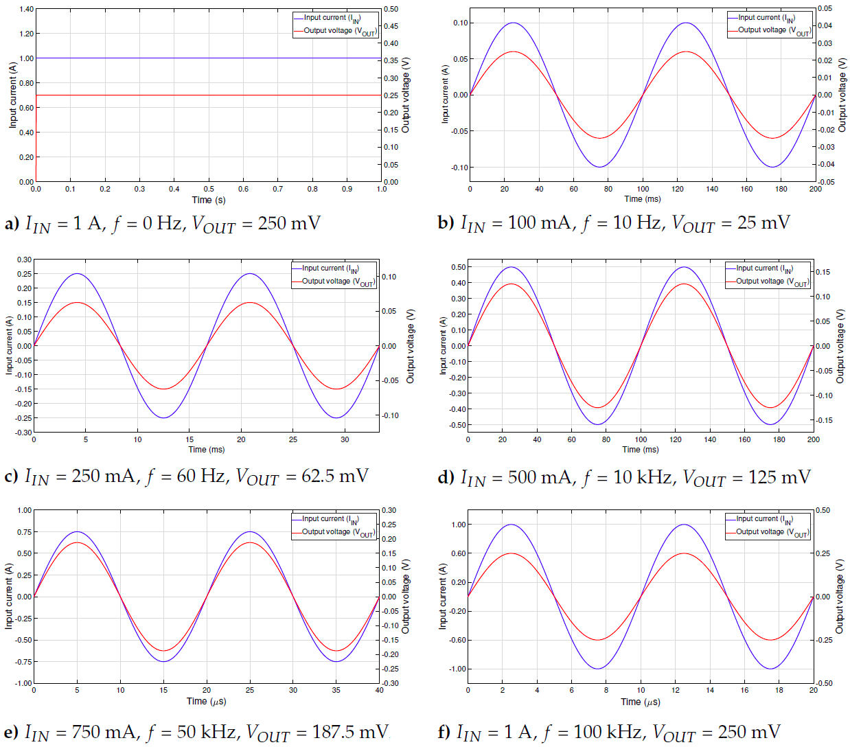
TABLE VI Amplitude relative error of the output current regarding input current.
| Frequency (kHz) |
IIN (A) |
VOUT (mV) |
TF (mΩ) |
IOUT (A) |
Relative error
(µA·A-1) |
| 0 | 1.00 | 250.000 0 | 249.999 997 | 1.000 000 | 0.0 |
| 0.010 | 0.10 | 25.000 0 | 249.999 997 | 0.100 000 | 0.0 |
| 0.060 | 0.25 | 62.500 0 | 249.999 997 | 0.250 000 | 0.0 |
| 10 | 0.50 | 125.000 0 | 249.999 997 | 0.500 000 | 0.0 |
| 50 | 0.75 | 187.500 0 | 249.999 998 | 0.750 000 | 0.0 |
| 100 | 1.00 | 250.000 2 | 250.000 000 | 1.000 001 | 0.8 |
Table VI summarizes the performance of the RCT in terms of input current level and the frequency of the current. It is shown that the RCT exhibits a good performance based on the small relative error of nearly 1 ppm at 1.0 A and 100 kHz, as shown in the last column of Table VI.
3.3. Performance of the RCT under harmonic noise
As it is known, the most common non-linear loads currently available are the Compact Fluorescent Lamps (CFL). Nowadays, these devices are replacing the Incandescent Bulbs (IB) because of their higher energy efficiency, but they generate highly distorted current waveform during their operation due to the AC to DC conversion process on its electronic ballast. Therefore, the methodology followed in this work is injecting a highly distorted signal to the TF of the RCT to evaluate its response. According to the definition, the total harmonic content of a waveform is compared regarding its fundamental, as expressed by Eq. (23) [46], where n represents the harmonic order. It is a measure of how much the current waveform is distorted, compared to the current, from a purely resistive load.
The highly distorted CFL current waveform was obtained from a high-accuracy analog-to-digital sampling system designed by the Centro Nacional de Metrología - México, CENAM [47]. The CFL was fed at the line frequency of 60 Hz. A high-precision current shunt was connected in the current path to provide a voltage signal for the sampling system. The sampling system frequency was programmed to 61.44 kHz, which allowed having 1,024 samples per cycle of the sampled signal. The observation window of the sampling system is 1 s. Figure 18 presents the CFL current waveform applied to the TF of the RCT, the output voltage waveform obtained, and the IB current waveform to observe the degree of distortion of the CFL current waveform compared to that generated by a resistive load, as in an IB. Note that due to the highlinearity and wide bandwidth of the RCT, the output voltage has the same shape as the input current.

A custom algorithm designed by CENAM was used to obtain the amplitude and the phase components of the sampled waveform. The algorithm is based on the Interpolated Discrete Fourier Transform (IDFT) with spectral leakage mitigation for non-coherent sampling. The method estimates correctly the values of magnitude and phase components at part-per-million levels from the maximum energy that provides the DFT without it being necessary to occupy analytical approximations of the spectral response of the signal under study [47]. The CFL current waveform has a THD of 89.8 %, and a fundamental component and ninety-nine harmonics components form it. The amplitude of the fundamental component is 0.277 5 A. The even and odd harmonic components have a percentage relationship concerning the fundamental component in the range from (0.1-0.3) % and (0.369.4) %, respectively. The amplitude and phase components of the input current and output voltage can be observed from Figs. 19a) to 19d).
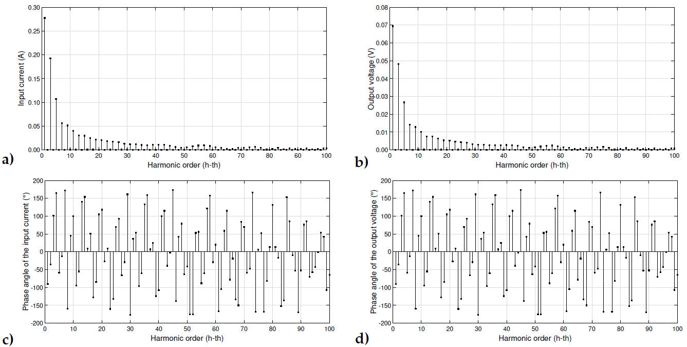
FIGURE 19 Results of the frequency analysis of the RCT. a)Input current amplitude components. b)Output voltage amplitude components. c)Input current phase angle components. d)Output voltage phase angle components.
A comparison of the amplitude and phase components between the input current and the output voltage are presented in Figs. 20a) and 20b), respectively.
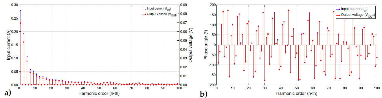
FIGURE 20 Comparison of the amplitude and phase components of the input current and the output voltage. a)Amplitude components. b)Phase angle components.
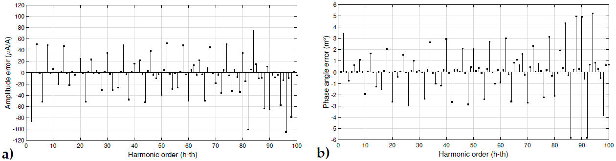
The relative amplitude error of each harmonic component of the output current regarding the input current is computed by Eq. (22), and they are shown in Fig. 21a). The most significant amplitude errors are presented when the harmonic component has a percentage relationship concerning the fundamental component in the range from (0.1-0.3) %. The phase angle error of the output current regarding the input current is computed by Eq. (24), and they are shown in Fig. 21b). The most significant phase errors are presented under the same conditions of amplitude percentage, as stated previously.
4. Conclusions and future work
This work describes the design process followed to build an RCT, based on the thermal and electrical characteristics of all its components. Of particular interest to the metrology community is the fact that this transducer is a good proposal for the measurement of highly distorted current waveforms at relatively high current levels of 1 A. The design of the transducer as shown in this paper highlights some benefits, like an improved heat transfer mechanism that greatly reduces the effects of self-heating without compromising the heat time constant, neither the frequency response of the transducer for the purposes of avoiding self-heating losses and achieving an outstanding frequency response, respectively.
As shown in the paper, the design of the RCT allows grouping all the components of the transducer into two categories. First, a customized system was considered for the management and conduction of the heat generated inside the RCT towards the surrounding environment. Second, concerned the determination of its frequency response obtained from an appropriate electric model. For both analyzes, the geometries, sizes, and thicknesses were defined through an iterative process to minimize and quantify the heat losses, thus reducing the frequency dependence of parasitic inductances and capacitances through the current path.
The linear bandwidth of the RTC makes it ideal for the measurement of highly distorted low-consumption current signal and other applications i.e., active pulse width modulation rectifiers, and light-emitting diode lamps, etc., where it is possible to determinate the amplitude and phase errors of the RCT throughout its operating range from DC to 100 kHz from its electric model.
Although the thermopile output voltage is only 37 mV at full scale, it is beneficial for monitoring the status of the RCT. Additionally, it can be used as a ratio between both output voltages signals available and have a redundancy method in critical electric current monitoring processes.
As future work, the next stage is the construction and characterization of the RCT designed and modeled in this work, and subsequently, increase its current capacity and bandwidth up to 10 A and 10 MHz, respectively.
Author contributions
Sergio Campos-Montiel designed the prototype, performed all computation and the simulations, analyzed the data and wrote the paper; L. Lira reviewed, edited, and provided technical advice to this manuscript; S. Jiménez-Sandoval and René Carranza-López-Padilla provided supervision, project administration, reviewed, edited, and contributed technical advice to this work.
Funding
This project was funded by Centro Nacional de Metrología, CENAM-México.

