


 nova página do texto(beta)
 Inglês (pdf)
 Artigo em XML
 Referências do artigo
 Enviar este artigo por email
 Citado por SciELO
  Similares em
SciELO
Similares em
SciELO 
 Permalink
1.Introduction
Gallium nitride (GaN) is an important wide bandgap (3.39 eV) III-V semiconductor material, which is widely used in the field of ultraviolet detection, photolysis water, and field-effect transistors 1-6. Traditional ultraviolet (UV) detectors based on silicon require additional filters, which increases the cost of ultraviolet detectors. However, GaN with wide bandgap is sensitive to ultraviolet light and hardly responds to visible light.
At present, the manufacturing of commercial devices is mainly based on two-dimensional materials. GaN films are usually deposited by the MOCVD method to fabricate devices. However, one-dimensional nanomaterials have more unique electronic and optical properties, which are more conducive to improve the performance of the ultraviolet detector. There are various methods to grow GaN nanowires(NWs), including metal-organic chemical vapor deposition (MOCVD) 7, 8, molecular beam epitaxy (MBE) 9-13, and chemical vapor deposition (CVD) 14-23. Among these methods, CVD is the most effective method to synthesize nanowires. CVD method has great flexibility in the synthesis of GaN nanowires. Ga2O3 or metal gallium is commonly used as source materials 2, 14. Si and sapphire are used as a substrate for deposition. The change of source material and substrate can affect the morphology of nanowires. In general, the sidewalls of nanowires grown by CVD are relatively smooth 4, 18. Although previous studies have shown that serrated GaN nanowires have been synthesized with Ga2O3 as the source materials 24, there are few related studies using gallium as the source materials to synthesize it.
UV detector based on Gallium nitride is not widely used because of its high cost. In previous studies, Au and Ni were often used as electrode materials in contact with GaN nanowires 3, 6. However, there are few studies on the GaN UV detector based on the copper (Cu) electrode. Copper is a cheap material with low resistivity (1.75 x 10⁻⁸ Ωm) , which can reduce the cost of the detector. The work function of copper is 4.65 eV, and it is easy to form an ohmic contact with GaN. Therefore, the study of the GaN UV detector based on Cu nanowires is of great significance.
An ultraviolet detector based on GaN nanowires is reported in this paper. Serrated GaN nanowires were grown by the CVD method, and Cu nanowires were synthesized by liquid-phase reduction method. The ohmic contact between GaN and Cu nanowires is realized. The detector exhibits a photo-to-dark current ratio of 18.3 under 365 nm light illumination.
2.Experimental section
2.1.Synthesis of nanowires
GaN nanowires were synthesized on a sapphire substrate by a CVD method. To assist the growth of nanowires, Au was used as a metal catalyst. Au film was deposited on the sapphire substrate by magnetron sputtering system. Metal gallium and ammonia gas are used as source materials. Gallium and the sapphire substrate are placed in quartz boats, respectively, and then the quartz boat is placed in a quartz tube furnace. The substrate is placed downstream of gallium, and the distance between gallium and substrate is 2 cm. The residual oxygen in the furnace was evacuated by purging carrier gas into the furnace for 10 min. Then, the interior of the quartz tube is evacuated, and the furnace was heated to 900 at 20oC per minute. When the temperature rises to 900oC, carrier gas(Ar) and ammonia gas are transported to the furnace. The flow rates of NH3 and Ar were 30 and 10 sccm, respectively. The growth of nanowires duration lasted for 30 min; after that, Ar gas is introduced to remove residual ammonia in the furnace.
The Cu nanowires were synthesized by a liquid-phase reduction method. In a typical process, 1 g copper acetate and 1 g polyvinylpyrrolidone(PVP) were dissolved in 100 ml deionized water. Then 4 g ascorbic acid was dripped into copper acetate solution under stirring. After that, the solution was stirred in a sealed container, at 80oC, for 1 hour. During the period a transition of color from yellow to red could be seen. Finally, the product obtained by centrifugation is copper nanowires.
The synthesized samples were characterized. The surface morphology of the samples was observed by field emission scanning electron microscopy (FESEM). The TEM images of GaN nanowires were obtained in the JEM-2010 FEF transmission electron microscope. The crystal structure of the samples was characterized by high resolution X-ray diffraction (HR-XRD). The composition of GaN nanowires was characterized by X-ray photoelectron spectroscopy (XPS).
2.2.Fabrication of Device
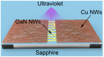
Copper was used as electrode material in the manufacture of a UV detector. Sapphire was used as a substrate of the device, and GaN nanowires were used as a photosensitive material. GaN nanowires were deposited on the sapphire substrate, and Cu nanowires were dripped on two ends of the substrate.
Figure 1 shows the schematic diagram of a UV detector based on GaN nanowires.
The I-V characteristics of the UV detector were characterized under dark and different wavelengths of light illumination using a Keithley 4200 instrument. The ultraviolet light source is a xenon lamp with a filter.
3.Results and discussion
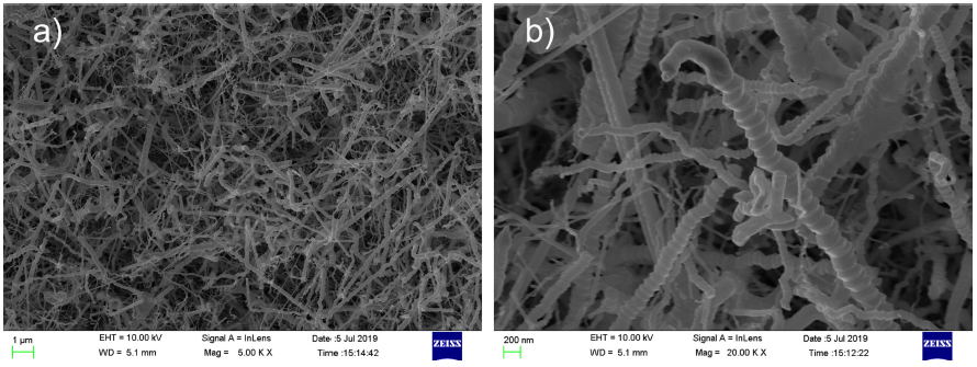
The surface morphology of GaN nanowires was visualized by FESEM. As shown in Fig. 2(a), serrated GaN nanowires are synthesized on the sapphire substrate by a CVD method. The length of GaN nanowires ranges from several microns to tens of microns. Figure 2b) shows that GaN nanowires are serrated. The study found that the growth of the serrated nanowires occurs through a Ga-rich droplet under N-deficient conditions 24. So the growth of large diameter nanowires is nitrogen deficient, and the nanowires are serrated. As can be seen from Fig. 2b), the morphology of some nanowires is not serrated. This is due to the larger specific surface area of small diameter nanowires, which reduces the degree of nitrogen deficiency. The smaller the diameter of nanowires, the smoother the sidewall.
Figures 3a) and 3b) shows the TEM image of serrated GaN nanowires. Figure 3b) shows that the diameter of the nanowires is about 200 nm and changes periodically. Figure 3c) and 3d) show the HRTEM image of serrated GaN nanowires, which reveal the lattice fringes with an interplanar spacing of 0.26 nm, corresponding to the (002) planes of hexagonal wurtzite GaN. Therefore it can be confirmed that the GaN nanowires grow along [001] direction. Figure 3c) shows the lattice-resolved TEM image of the convex part and Fig. 3d) shows the lattice-resolved TEM image of the concave part. As shown in Fig. 3c) and 3d), the interplanar spacing and orientation of the lattice fringes are the same, which indicates that the nanowires are single-crystal.
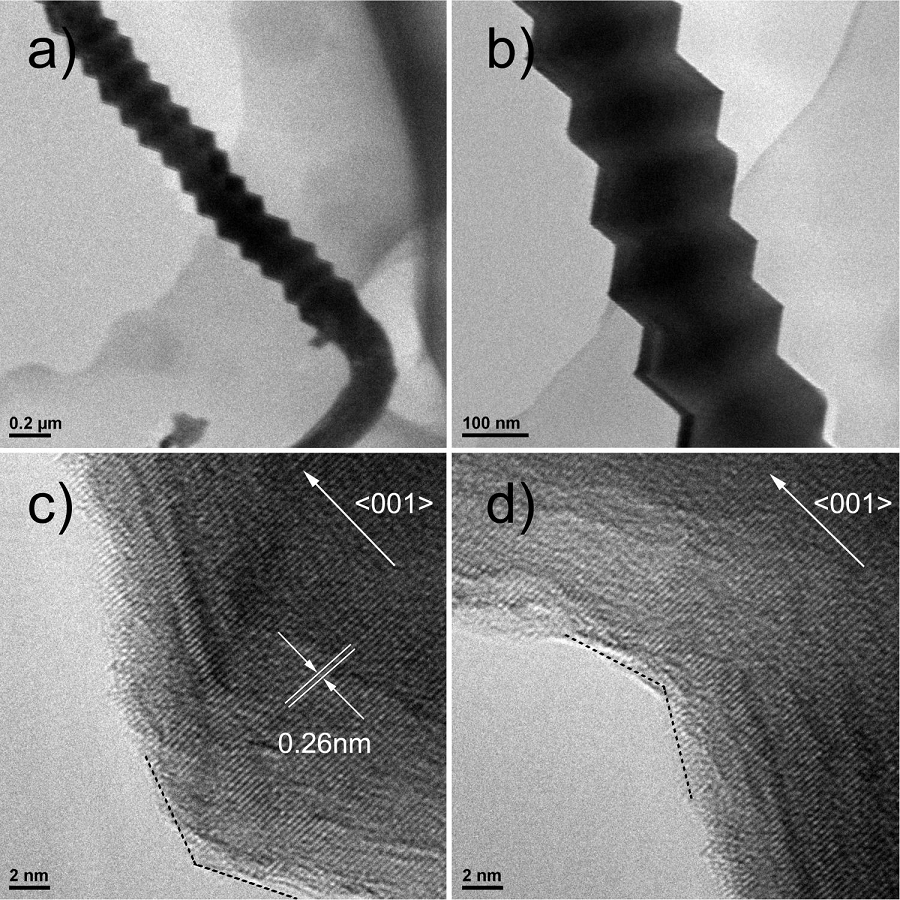
Figure 3 a) and b) TEM image of the serrated GaN nanowires; c) and d) lattice-resolved TEM image of the nanowires.
The growth process of serrated GaN nanowires is shown in Fig. 4. Vapor-liquid-solid(VLS) mechanism is used toexplain the growth of serrated GaN nanowires. Figure 4a) shows the process of the diameter of the nanowires increasing. Under the condition of Ga-rich, the volume of Au-Ga alloy droplets increases gradually. The nanowires grow along the edge of the alloy and the diffusion of Au-Ga alloy droplets at high temperature leads to the increase of nanowires’ diameter. With the increase of nanowires’ diameter, the alloy droplet is stretched on the contact surface. When the alloy droplet is stretched to the limit, the diameter of nanowires increases to the maximum. Then, the diameter of the nanowires decreases gradually. Figure 4b) shows the process of nanowires’ diameter decreasing. With the increase of the droplet surface area, the surface tension of the droplet causes the droplets to contract, which causes the diameter of the nanowires to decrease gradually. According to such a crystal growth model, the nanowires grow periodically, and finally, serrated nanowires are synthesized.
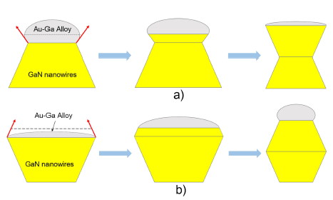
Figure 4 The growth process of serrated nanowires: a) increase of nanowires diameter; b) decrease of nanowires diameter.
Figure 5 shows the X-ray diffraction pattern of GaN nanowires. The XRD diagram reveals the diffraction peaks of (100), (002), (101) corresponded to the hexagonal wurtzite GaN. As shown in Fig. 5, the X-ray diagram exhibited a sharp and narrow diffraction peak of (002) indicated the nanowires prefer to c-axis orientation. Because the (002) plane of GaN has the lowest surface energy density, and the growth of other planes is limited 2.
The surface composition of GaN nanowires was determined from the XPS spectra. Figure 6 shows the room temperature XPS survey spectrum of GaN nanowires. The identified peaks represent the core levels associating with gallium, nitrogen (N 1s), carbon (C 1s), and oxygen (O 1s), respectively. The (Ga 2p) peaks shown in Fig. 6c) illustrates the presence of gallium in a compound state 25. The observed Ga 3d peak indicates the absence of oxygen, which is evidence of the absence of Ga-O bond formation 4. The (N 1s) peak indicates the presence of nitride contents in the samples. Due to N-H bond formation, an asymmetrical peak, as shown in Fig. 6b) is observed for (N 1s) 4. The detection of (O 1s) peaks are attributed to the external pollution of the sample. The composition of the sample can be determined as GaN by XPS spectra.
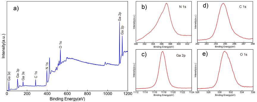
Figure 6 a) Room-temperature XPS survey spectrum of GaN nanowires; b) the binding energy of (N 1s); c) the binding energy of (Ga 2p); d) and e) the binding energy of (Ga 2p) and (O 1s).
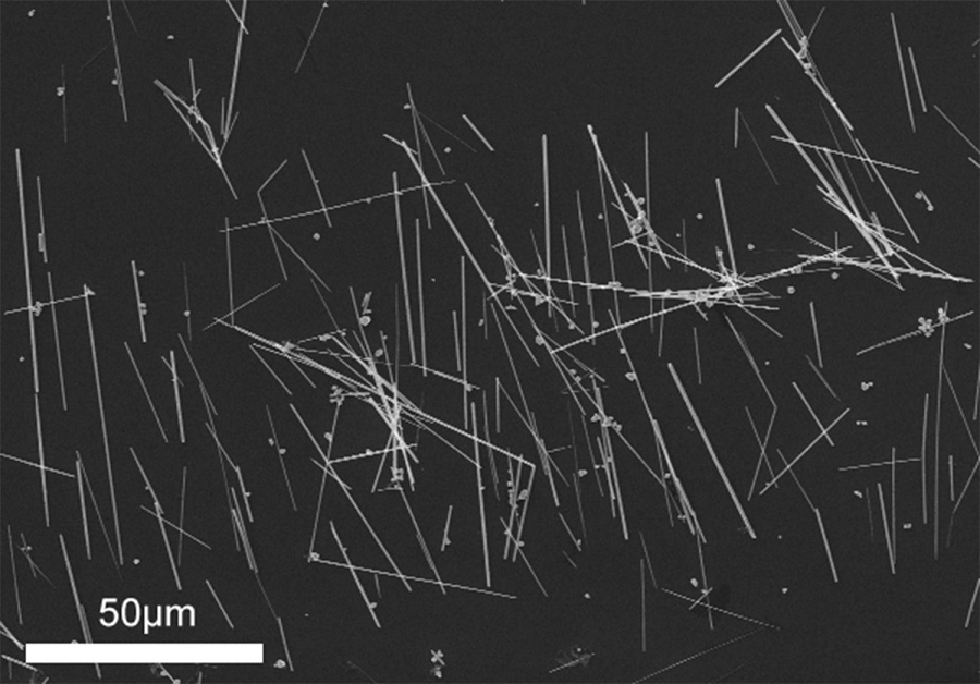
Figure 7 shows the SEM image of the Cu nanowires. The SEM image shows that the samples contain nanowires and a few particles. The average length of typical Cu nanowires is about 30 μm. The growth mechanism of nanowires is as follows: at first, some small nanoparticles gradually dissolve in the solution to generate free copper atoms, and then these copper atoms transfer to some large crystal surfaces with high surface free energies. Finally, copper nanowires are formed 26, 27.
Generally, Al is used as metal material to form an ohmic contact with GaN in industry, and the Al atoms are diffused to the surface of GaN by high-temperature annealing to reduce the contact resistance. Therefore, some Cu atoms diffuse to the contact surface of GaN and Cu, reducing the resistance of the contact surface, which is conducive to the fabrication of the detector. Figure 8 shows the I-V characteristics of the UV detector measured under dark and light illumination of different wavelengths. I-V characteristics show that ohmic contact is formed between the Cu electrode and GaN nanowire. It is found that photocurrent increases with the decrease of light wavelength. It can be seen from Fig. 8 that the device has a very low photocurrent for visible light with wavelengths of 550 nm and 645 nm, and a greater response for violet light with wavelengths of 450 nm. The inset in Fig. 8 shows the response curves in the log scale of the detector and the 365 nm light exposure resulted in the maximum photocurrent comcompared to that of other wavelengths. The current of the detector increases from 5.6 nA to 108 nA under 365 nm UV illumination at 5 V bias. The response of the detector in the wavelength greater than 365 nm can be attributed to the defect of nanowires 2.
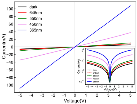
Figure 9 shows the photocurrent-time responses of the UV detector under 365 nm UV illumination at 5 V bias. It can be found that the photocurrent increases rapidly after the UV light is turned on, and then increases slowly. When the ultraviolet light is turned off, the current drops rapidly then drops slowly. The photocurrent-time response of the device is identical in six cycles, as shown in Fig. 9a), which illustrates that the device has repeatability. Figure 9b) shows the photocurrent-time response in a cycle. It can be seen from Fig. 9b) that the photocurrent increases rapidly from 23 nA to 100 nA in 4 seconds after the UV light is turned on.
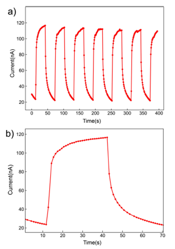
Figure 9 a) Photocurrent-ime responses of the UV detector under 365 nm UV illumination at 5 V bias; b) Photocurrent-time responses in a cycle.
The unintentionally doped gallium nitride exhibits strong n-type conductivity due to the defect of nitrogen-vacancy. The conductivity of gallium nitride in this paper is about 0.024 S/m. The manufacture of high resistance gallium nitride is still a difficult problem in the industry. Table I shows the performance comparison of GaN-based photodetectors. Compared with the reported photoconductive detector, the photo-to-dark ratio of the detector is significantly increased from 8 to 18.3 3.
4.Conclusions
In summary, serrated GaN nanowires were successfully synthesized on the sapphire substrate by chemical vapor deposition. The study found that the diffusion and surface tension of Au-Ga alloy droplets causes the growth of serrated nanowires, and the growth of serrated nanowires is more favorable under the condition of Ga-rich. Copper nanowires with a length of tens of microns were prepared by liquid-phase reduction method, and the detector based on copper and GaN nanowires was prepared. The responses of the ultraviolet detector varies with the wavelengths of light, which shows that the detector has selectivity for different wavelengths of light. The detector exhibits a photo-to-dark current ratio of 18.3 for 365 nm ultraviolet illumination, and the response wavelength is consistent with the wavelength corresponding to the bandgap width of GaN.

