


 nueva página del texto (beta)
 Inglés (pdf)
 Artículo en XML
 Referencias del artículo
 Enviar artículo por email
 Citado por SciELO
  Similares en
SciELO
Similares en
SciELO 
 Permalink
1.Introduction
The Data Processing Electronics Interface described here is designed to acquire and process 10-bit signals for avalanche photodiodes (APDs) [1] with a metal resistor semiconductor and a Hamamatsu R6095 photomultiplier (PMT) [2] integrated in a plastic scintillator particle detector. The interface’s architecture contains several blocks to avoid typical perturbations due to temperature variation in electronics, detectors, and induced noise. The data processor system is able to perform a continuous read out, identify a valid signal pulse, reject glitches, and compress the data without any loss of information. The signals are compressed in the data compression block which removes all data below a predefined voltage threshold and identifies a pulse when three consecutive data values are over the threshold. Each pulse is tagged with a time stamp, number of samples, and event number for reconstruction purposes. All pulses are formatted and stored in a multi-event buffer with a bandwidth of 200 Mbytes/s. In continuous mode, the maximum input data rate is 40 MHz, where all the signals coming from the analog-to-digital converts (ADCs) are stored in a dual port memory. The maximum read frequency for the dual port memory is 300 MHz. The interface can generate a calibration signal that allows to detect errors in any of the blocks. The system has been tested with particle detectors based on APDs and photomultipliers (PMTs) triggered with atmospheric muons. The interface is designed to process large data volumes without any loss of information. The output signal is the same regardless a PMT or an APD is connected to the input of the interface. The maximum rate expected for a single channel is about 260 bits/event with up to eight channels allowed in a single FPGA interface.
2. Materials and methods
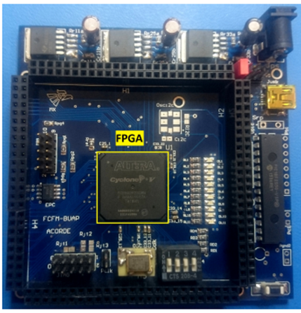
A front-end electronic card (FEE) is designed to digitize the signals from the PMTs and APDs. This FEE, in Fig. 1, is composed by a charge preamplifier, a 4th order shaping amplifier and a 10 bit 40 MHz ADC.

Up to eight FEE cards can work in parallel connected to a single interface card.
Since the output data are 10-bit wide, all of the FEE signals would require 80
inputs and 8 dedicated output from the field-programmable gate arrays (FPGA), which
are the maximum number of I/O’s on it. The 8 dedicated outputs are required to
distribute the clock signals for each FEE to synchronize the operation and data
transfer without jitter issues. The data processing interface card we designed is a
The firmware of the interface consists of the five main blocks shown in Fig. 3: a) the Ring Buffer is a dual port memory
[3] of
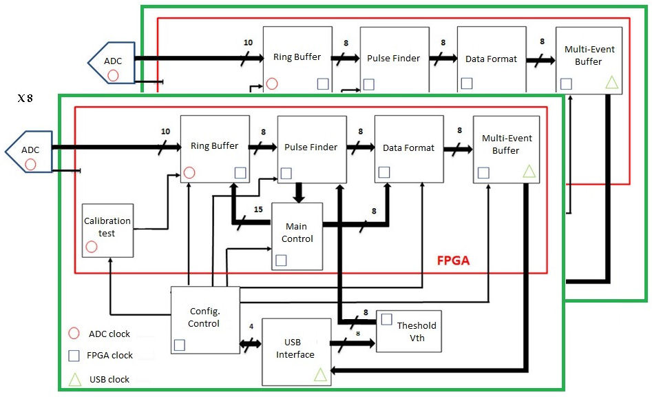
Figure 3 Schematic diagram of the Interface Board firmware. There are three clock domains controlled by an internal Phaselocked loop (PLL) in the FPGA. All the blocks run in a clock domain two times faster than the writing frequency of the Ring Buffer to assure there is always free space for continuous data acquisition.
2.1.Ring Buffer
The Ring Buffer is a dual-port memory designed to continuously store all the digitized signals in order to avoid loss of information. The read access speed is always twice the write access speed to ensure availability of memory space to continuously write data. The maximum read and write access of the dual port memory is 300 MHz but we are running only up to 80 MHz. There is one Ring buffer for each channel while the maximum number of channels allowed is eight.
2.2.Pulse Finder
The Pulse Finder compares each channel’s data from the Ring Buffer with a programmable threshold generating a hit and identifying a signal whenever it detects three consecutive samples over the threshold. This condition allows to discriminate valid pulses from any glitch.
2.3.Event format
The Data Format block constructs the internal data format for valid pulses and empty events. The data format for a valid pulse is composed of a start of event value that identifies each pulse, the channel number, a time stamp with respect to the previous pulse, the payload, the data length, and the number of data. For an empty event, the data format is composed of a start of data value, the channel number, time stamp, the data length, and the data number. The empty events are inclu-ded only if the maximum waiting time for a valid pulse has elapsed; the purpose of this is to preserve time continuity and to identify the exact time when a muon is detected with respect to the internal clock of the FPGA. Figure 4 shows the internal data format for empty and valid events.

2.4.Multi-Event Buffer
The Multi-Event Buffer block is an
2.5.Main Control
The Main Control block receives and distributes the configuration settings for the data processing. The distributed parameters are the active channels, the reference threshold, the start and stop data process commands and the auto-test procedure command. The Main Control block synchronizes the operation of all the modules and triggers the sequences to process the data when specific signals are generated by each module.
3.Results
Digitized signals from cosmic rays in plastic scintillating detectors [6] are used as data source to test the interface; these detectors are the same used for the cosmic ray detector (ACORDE) [7]. The digitized signals come from a 10 bit 40 MHz ADC. The analog to digital conversion is activated by the Main Control Block. The maximum input signal rate that the system can handle is 10 KHz for both PMTs and APDs. The data processing interface is able to acquire digital signals through the implementation of the following functions in the FPGA’s firmware: clock distribution, configuration for the data acquisition, data formatting, and transfer to an external storage system. The system can also generate a test signal for calibration purposes. The signals from the ADC are 650 ns wide and are sampled at a rate of 20 MHz. Figure 5 shows the user interface of the acquisition system.

The connection button between the interface and the data acquisition system (DAQ) system is indicated with the number 1 in the figure, number 2 indicates the discriminator voltage input field for all the acquisition channels, number 3 is the button to enable the data storage in a specific file, and number 4 is the graphic area to display all the data from the FEE cards.
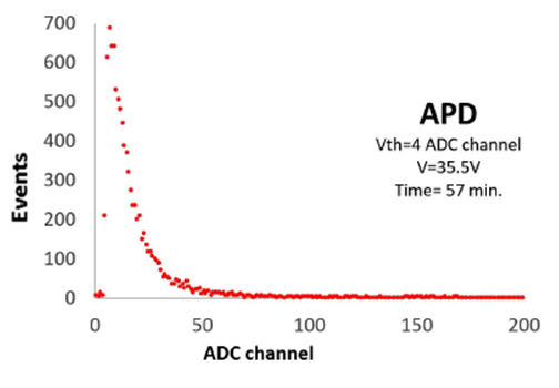
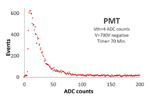
Besides processing and storing all the digitized signals, the maximum value of each signal is also measured and recorded. Figures 6 and 7 show the amplitude distribution for APD and PMT signals, respectively. For APDs the threshold was set to 4 ADC counts, the duration of the test was 57 minutes and the optimum bias Voltage 35.5 V. For the PMT, the discrimination threshold was 4 ADC counts, the duration of the test was 70 minutes and the optimum operational Voltage was 700 V.
A test signal of amplitude 714 ADC counts is stored in the firmware. One hundred thousand events with this test signal were injected to the FPGA during a period of 14 hours. The amplitude distribution of these events is shown in Fig. 8 where it is clear that the system does not register events of an incorrect amplitude.

4.Discussion
We can observe that the threshold level was the same for the PMT and the APD. It is usually expected for APDs to be noisier than PMTs; nevertheless, the FEE cards are able to drive the signals from both detectors. When an interruption occurs in the data transfer, the processing interface pauses the operation, only to be resumed when the resources become ready. During this pause period, the processing interface does not interrupt the data acquisition from the ADCs preventing any data loss. In addition, if the USB data transfer is stopped, the interface is capable of taking data for 1 more minute, since the Ring Buffer is able to write data even if the reading part is paused. Finally, the power consumption of the card in standby mode is 100 mA while for each active channel the card consumes 80 mA. Only one 5 V symmetrical power supply is needed to power the system.
5.Conclusions
The FPGA based Processing Interface we designed and built was successfully used to read-out, discriminate, digitize, and transfer signals produced by PMTs and APDs coupled to scintillating plastic detectors. This board is the first prototype based on a FPGA for application in cosmic ray and high energy physics. This interface is an excellent, easy-to-use option for scintillation detectors characterization. Its reduced size makes it ideal for applications where the space and access to the detector area are restricted. The Processing Interface is a novel way for reading out and store data from plastic scintillator based detectors. It is also well suited to test and verify the correct performance of a specific section in a multichannel or single channel detectors. The Pulse Finder module included in the firmware makes an external trigger detector unnecessary. A limitation of this prototype is that only eight channels were implemented for multichannel applications though this is clearly a drawback that can be overcome.

