


 text new page (beta)
 English (pdf)
 Article in xml format
 Article references
 Send this article by e-mail
 Cited by SciELO
  Similars in
SciELO
Similars in
SciELO 
 Permalink
1.Introduction
CuInSe2 (CIS) ternary semiconductor material has been used in the fabrication of the second generation of solar cell devices 1-8, because of the high optical absorption coefficient of more than 104 cm−1 6, good photostability 9, excellent longevity 9,10. The CIS semiconductor is a p-type with mobility of hole about 165 cm2/V.s 11. It has been used in thin film solar cell fabrication since 1953 and has been developed since then arriving at an efficiency of 19.5% 12. Also, p-type CIS has been combined with n-type TiO2 to form heterojunctions and has been tested for solar cell applications 12,13; however, the achieved efficiency did not the exceed 1.5×10−512. Furthermore, CIS has been used for fabrication of dye-sensitized solar cells (DSSC), forming a tandem cell with an efficiency greater than 15% 14. Efforts have targeted to control the morphology of the CIS nanocrystals such as; dots 15,16, spheres 10,17, flowers 18,19, tetrahedrons 20, hexagonal plates 7,21, octahedrons 22, or wires 23. Also, considerable work has mentioned the controlling of the composition 10,24,25, and crystal structure 17,26 of CuInSe2 NCs besides, achieving good monodispersity. Allen and Bawendi have synthesized CIS QDs with controlling the emission between red and near-IR. CuX and InX were heated with oleylamine (O.A) and trioctylphosphine (TOP) at 280-360∘C, then a solution of bis-(trimethylsilyl) selenide in TOP was addedm, the CIS NPs grow at a temperature ranged from 200 to 280∘C (16). In their method, a mixture of CuI and InCl3 dissolved trioctylphosphite, and selenium dissolved in trioctylphosphine were mixed in presence of hexadecylamine (HDA) as a surfactant at 320∘C. Tang et al. synthesized nearly the monodisperse CuInSe2, CuGaSe2, and CuInGaSe2 NPs in the presence of oleylamine as a capping agent using Cu, In, Ga salts, and Se powder 10. Chuan-Sheng Chiou et al., synthesized CIGS Chalcopyrite NPs using a solvothermal method 27. In their method; a mixture of ethylenediamine and Cu, In, Se and Ga(NO3)3 were added in an autoclave at a temperature of 200∘C for 36 h. The obtained CIGS were characterized using XRD, TEM, SEM, ICP-mass spectrometer. Chang et al. synthesized 1D and 3D CIS NPs using the oriented attachment mechanism and ligand protection approach 18. In their approach, a mixture of TOP, TOPO, and aliphatic amine was used as both stabilizer and reaction solvent. This synthetic route is suitable for the preparation of 1D nanowires, 3D nanoflower, and multipod nanostructures at different growth conditions 18. Also, flower-like ternary CIS microstructure with size ranging from 25 to 30 mm and thickness of 150 nm was prepared via a solvothermal route by Chen et al. at 180∘C at which, ethylenediamine was used as both reducing reagent and solvent 19. CIS nanorods of diameter about 50-100 nm and with length up to a few micrometers have been synthesized solvothermally using Ethylenediamine as a reaction solvent. The CIS nanorods stem grow from the complex [Cu(H2NCH2CH2NH2)2]+ which works as a template to react with InSe2 −for the growth of 1D nanostructures (28]. Korgel was synthesized CIS with trigonal pyramidal shape and narrow size distribution using selenourea as a Selenium precursor, oleylamine as both reducing reagent and solvent at controlled reaction temperature. InCl3 and CuCl were mixed with oleylamine, then heated up to 130∘C. Selenourea was injected after decreasing the temperature to 100∘C. The reaction temperature was raised again to 240∘C and kept for 1h 25. Yonglan Luo et al. were synthesized CIS and CGS hexagonal microplates in a mixture of oleic acid and oleylamine 12. Sharma et al. were prepared ternary CIS nanocrystals passivated with a mixture of aniline and 1-octadecene as a capping agent and were dispersed in a matrix of conducting polymer poly(3-hexylthiophene) 29.
We developed single pot chemical synthesis to control the shape of CuInSe2 nanoparticles. Through our method, the particle morphology depends only on the reaction temperature. CIS nanodots, nanorods, and nanoflowers had been prepared using the same precursors at different temperatures. This method is important because it allows us to study the optical, electric and photoelectric properties of the particles and their dependence on the morphology because all the different morphologies prepared in the same environment and have the same capping materials.
Then the different shapes of CIS nanoparticles were introduced to the DSSC to study their effect on the optical switching properties.
2.Materials and method
2.1.Chemicals
Copper(II)acetylacetonate (Cu(acac)2, Merck), Indium(III) chloride (InCl34H2O, Aldrich), Selenium powder (Se, Strem), technical grade Trioctylphosphine (TOP, Aldrich, 90%), technical grade oleylamine (Aldrich, 70%), Methanol (CH3OH, Aldrich), and Toluene absolute (C6H5CH3, Sharlu), Acetone (CH3COCH3, Aldrich), n-Hexane (CH3(CH2)4CH3, Aldrich, 99%), Hydrochloric acid (HCl, Fluka, 37%), Nitric acid (HNO3, Aldrich, 70%), were used as supplied.
2.2.Synthesis of CIS nanocrystals
The CIS nanodots wer synthesized typically as follows; A mixture of 0.2 mmol Cu(acac)2, 0.2 mmol InCl3⋅4H2O is dissolved in 15 ml of oleylamine in three-neck round flask, then the mixture is refluxed until reach to 160∘C. at this temperature, another solution of 0.4 mmol Se powder dissolved in a mixed solvent of (2 ml TOP and 24 ml oleylamine) is injected to the three-neck round flask. After about 60 min, the reaction is quenched by adding about 20 ml toluene. To separate the particles and purify them; 10 ml methanol was added to the three-neck round flask. The nanoparticles are flocculated and then separated from the supernatant by centrifugation. Dispersion of the flocculate in 2 ml of toluene, and 5 ml of methanol followed by further centrifugation then repeat this step to obtain pure NCs. The precipitated nanoparticles are dispersed in 5 ml hexane, and dried at 40∘C in the drying oven then collected as a powder. The CIS nanorods and nanoflowers are prepared by the same previous method of preparation except that the reaction temperature is changed, to 200∘C, 220∘C in case of nanorods and nanoflowers respectively.
2.3.1.Device fabrication
All cells were fabricated using ITO glass substrate. Two glass slides were used for each cell: one for the front electrode and the other for the back electrode. The TiO2 film was deposited on the ITO layer of one slide using the doctor blade method and then annealed in drying oven in normal atmospheric conditions for 30 minutes at 400∘C. The CIS nanocrystals were introduced directly on the TiO2 film using spin coating after that the glass slide was dipped in the hibiscus Dye. The back electrode was made by deposition of a carbon layer on the other slide by exposing the ITO to a candle flame. The iodide/triiodide electrolyte solution was introduced between the two slides and they were assembled together from both sides using a clamp.
2.4.Characterization
TEM and HR-TEM images of the samples were recorded using a JEM-2100 electron microscope operated at 200 kV equipped with High-resolution CCD Gatan digital camera for digital image processing. XRD measurements were carried out on a standard X’Pert Philips Materials Research diffractometer with Cu Kα1 radiation; the database used for the identification of crystal structures of materials investigated in this paper is the Joint Committee on Powder Diffraction Standards-International Center for Diffraction Data (JCPDS-ICDD) system. The Absorption spectra of the nanoparticles were recorded with a Perkin Elmer Lambda 35 UV/Vis spectrophotometer.
2.4.1.Evaluation equipments of the solar cells
A solar simulator of an irradiance of 1140 W/m2.
Cables
Keithley model 2400 digital source meter. It provides precision voltage and current sourcing as well as measurement capabilities, since during the testing; it can act as a voltage source, a current source, a voltage meter, a current meter, and an ohmmeter.
2.4.2.Evaluation Procedures of the Solar Cells
Connect the photoanode and back electrode of the fabricated solar cell to the Keithley 2400 positive and negative probes respectively by cables.
Expose the fabricated solar cell from the side of TiO2/dye electrode to the solar simulator Newport 69907 lamp in a way that the TiO2/dye electrode is under irradiation of the lamp meanwhile the Keithley measure the produced current coming from the cell and also measure the output produced voltage.
Set the resistance at different values by the Keithley multimeter.
As we noticed before; in each time we change the resistance (R), the voltage (V), and the current (I) is measured automatically by Keithley multimeter.
I=V/R
Plot voltage (X-axis) vs. current (Y-axis).
3.Results and discussion
The semiconductor nanoparticles have optical properties that attracted great attention due to it depends on the shape and size of the nanoparticles. So the optical properties of the semiconductor nanoparticles can be affected by some factors like size and shape, surface states, and composition, etc.
Figure 1 illustrate the progress of absorption spectra during typical CuInSe2 NC growth at different temperatures; 160, 200, and 220∘C. The absorb in a wide range in the visible region extend from 400 nm to 600 nm have a broad peak with a tail in the long-wavelength direction for that prepared at 200∘C and 220∘C, showing an excitonic peak at about 526 nm for that prepared at 160∘C. Compared to bulk CuInSe2 that have excitonic peak at about 1192 nm and an large exciton Bohr radius (r Bohr ) of 10.6 nm [30]; the quantum confinement effect (QC) is expected for some colloidal NCs that we have prepared, This could be proved by comparing the size of as-prepared nanoparticles to their corresponding r Bohr .
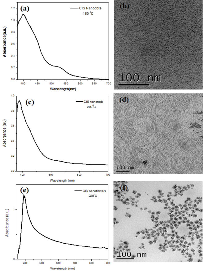
FIGURE 1 Absorption spectra of the CIS nanodots, nanorods, and nanoflowers (a, c, and e), and the corresponding TEM images (b, d, and f) respectively.
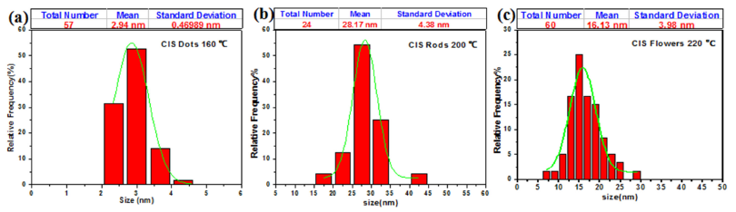
The corresponding TEM images in Fig. 1 show that the obtained nanoparticles at 160, 200, and 220∘C have dots, rods, and flowers-like shape with uniform size. By measuring the average particle size of the obtained nanoparticles in Fig. 2; it was found about 3 nm for the nanodots, this is smaller than the r Bohr of the bulk CuInSe2. This means that the QC is expected for the nanodots. Also, the average length and width of the nanorods were found about 28 nm and 4 nm respectively; so the width of nanorods is smaller than r Bohr of the bulk CuInSe2, and their length is larger than it. This means that the QC is expected for the width and not expected for its length of the nanorods. At the same time, by measuring the average particle size of the nanoflowers; it was found about 26 nm, it’s larger than the rBohr of the bulk CuInSe2. This means that the QC isn’t expected for the CuInSe2 nanoflowers. The differences in the density of nanoparticles for three different temperatures are appeared in the results, because of the size and the shape of nanoparticles.
It has been proved before that the reaction temperature has a huge effect on tuning the morphology of different types of NCs. In this work; concentration of the precursors and surfactants were fixed, and the experiments were conducted at different temperatures of 160, 200, and 220∘C respectively to investigate the reaction temperature effect on the shape of CuInSe2 nanostructures. We noticed that; after the reaction proceeding for 60 min at these different temperatures, the particle sizes and morphologies of the obtained nanoparticles differ, since the temperature can control the shape of the CIS to dots, rods, and flowers while the total size on the nanometer scale.
Thus, at reaction temperature 160∘C; the average size was approximately 3 nm with relatively good morphology and the monodisperse dots shape. As the reaction temperature increased to 200∘C, the morphology of the obtained nanoparticles changed to elongated rod-like shape with average length about 28 nm, width about 4 nm and with aspect ratio approximately 7. When the reaction temperature increased to 220∘C, the morphology of the obtained nanoparticles changed to a flower-like shape of average size about 26 nm, with few different shapes of prisms and hexagons; these observed in Fig. 1 and 2.
Generally, it was known that the growth of nanocrystals in solutions typically involves two processes: fast nucleation followed by growth into primary nanoparticles. After the primary particles were formed, the growth of nanoparticles may grow through two primary mechanisms: Ostwald ripening and aggregation. Ostwald ripening occurs by dissolving the smaller nanocrystals into a solution and growing them back onto larger ones among the distribution. Ostwald ripening does not sufficiently describe the growth of some systems where the primary particles were likely to aggregate into secondary particles through oriented attachments. In some cases, the formed secondary particles exhibit preferred structures such as wires, rods, flowers, or uniform spheres. This oriented attachment mechanism has been named by Penn and Banfield, it is also named as the direct self-organization of two particles into a single crystal by sharing a common crystallographic orientation 31,32. This oriented attachment can give rise to either homogeneous single crystals or to crystals separated by twin boundaries what is called imperfect oriented attachment. This type of oriented attachment when the particles of similar surfaces structures approaches, and there will be a driving force to form chemical bonds between atoms of opposing surfaces to get full coordination 31,32. However, in general, surfaces are not atomically flat so that the coherence will then be achieved by distortion in some areas of the interface, and edge dislocations or misorientation will form in the regions of step sites. This can occur when the number of surface ligands was not enough to protect all of the nanoparticles. Based on the above experimental results and the HR-TEM image; the produced CIS nanodots that prepared at 160∘C represent the basic unit or the inorganic nano building unit of these complex nanostructures (nanorods and nanoflowers).
As mentioned before, when the reaction proceeding at temperature 200∘C, there will be a driving force to form bonds between atoms of opposing surfaces of CIS nanodots “nano building unit” so as to achieve full coordination. This produces the formation of homogeneous single crystals in form of CIS nanorods by homogeneous oriented attachment since there are no twin boundaries between the primary particles this observed at the HR-TEM image, see Fig. 3. When the reaction temperature increased to 220∘C, also there will be a driving force to form bonds between atoms of opposing surfaces of CIS nanodots “nanobuilding unit” so as to achieve full coordination; however, in this case the CIS nanodots aggregated by imperfect oriented attachment to form CIS nanoflowers of a pendant-like structure due to presence of boundaries and defects which are usually absent in the particles formed by Ostwald ripening this observed at the HR-TEM images, see Fig. 4. The rod and flower Shapes may be formed due to the number of surface ligands was not sufficient to protect all of the nanoparticles; therefore the individual nanoparticles became unstable and aggregated into these obtained nanostructures 18.
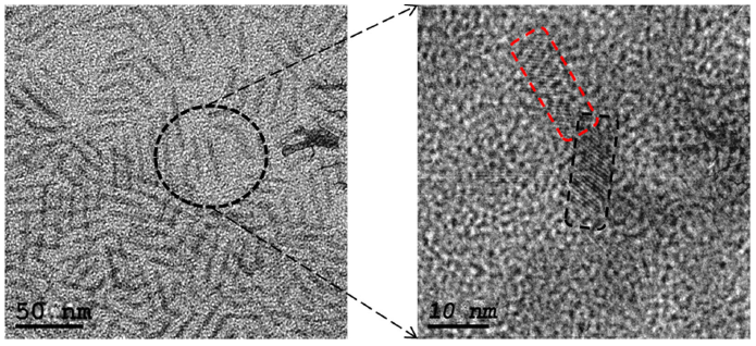
FIGURE 3 HR-TEM images of CuInSe2 Nanorods sample of different magnifications that shows the homogeneous oriented attachment mechanism.
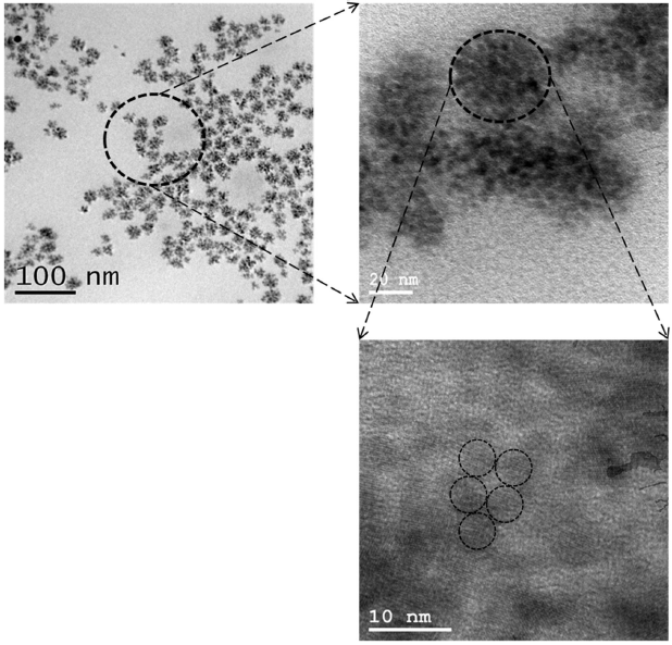
FIGURE 4 HR-TEM images of CuInSe2 Nanoflowers sample of different magnifications that shows the imperfect oriented attachment mechanism.
X-ray diffraction (XRD) patterns indicate that the as-prepared nanodots and nanorods have a tetragonal lattice structure; see Fig. 5. The tetragonal structure as shown in the (JCPDS-XRD Cards no: 00-023-0209) is characterized with three distinct features: the first at 2θ= 26.66∘ is due to the reflection of (112) planes, the second appearing at 2θ= 44.37∘ due to the reflection of (220) planes, and the third features appearing at 2θ= 52.45∘ due to the reflection of (312) planes. The shoulder at 2θ= 35.59∘ is due to the reflections of (211) planes. All these features appear in the (XRD) pattern of nanodots and nanorods. These results provide evidence that they have a tetragonal lattice structure.
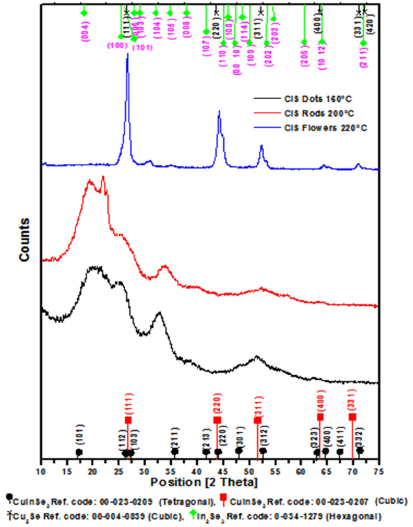
FIGURE 5 shows the XRD patterns of CuInSe2 NCs prepared at different temperatures; 160±C (black line) and 200±C (red line), and 220±C (blue line).
XRD pattern of the as-prepared CIS nanoflowers indicate that it has a cubic lattice structure; see Fig. 5. The cubic structure as shown in the (JCPDS-XRD Cards no: 00-023-0207) is characterized with three distinct features: the first at 2θ= 26.34∘ is due to the reflection of (111) planes, the second appearing at 2θ= 43.60∘ due to the reflection of (220) planes, and the third features appearing at 2θ= 51.78∘ due to the reflection of (311) planes. The shoulders at 2θ= 63.63∘ and 2θ= 69.820∘ are due to the reflections of (400) and (332) planes. All these features appear in the (XRD) pattern of nanoflowers; this provides evidence that; it has a cubic lattice structure.
3.1.Electrical characterization
Study effect of CuInSe2 nanodots, nanorods and nanoflowers on enhancing the photocurrent response of DSSC.
In this work, we need to study the effect of the different shapes of CIS nanoparticles on the photocurrent response or “the optical switching” of DSSC. Optical switching is the transient response of the short-circuit photocurrent to the on-off irradiation. This determines the stability of solar cells as well as the real electric current that can be extracted from it. Ideally, the response should be constant throughout the whole period when the a light is on. i.e. it means reaching a steady state. So we need to measure the settling time of the DSSC “which means the spent time by the cell to reach the steady state” in order to know the effect of CIS with different shapes on this phenomenon.
The I-V characteristic curves of the hibiscus-sensitized solar cell with CIS nanoflowers show a short circuit current very close to that obtained from the nanodots but with a small drop in the open circuit voltage. On the other hand, the nanorods didn’t give a good performance with a short circuit current, and the open circuit voltage concerning to the nanodots as shown in Fig. 6.
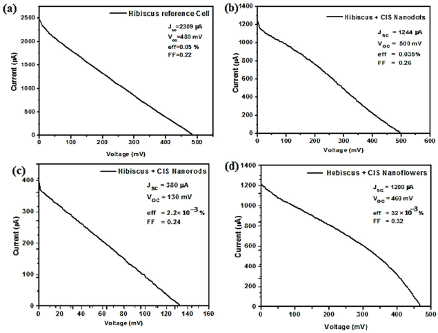
FIGURE 6 Shows the I-V characteristic curves of (a) hibiscus-sensitized reference solar cell, (b) hibiscus-sensitized solar cell with CIS nanodots, (c) hibiscus-sensitized solar cell with CIS nanorods and (d) hibiscus-sensitized solar cell with CIS nanoflowers.
The optical switching of the solar cell is shown in Fig. 7. Note that the settling time for the hibiscus-sensitized reference cell is more than 17 seconds as shown in Fig. 7a). Adding CIS nanocrystals enhanced the response considerably. CIS Nanodots reduce the settling time to 150 milliseconds, CIS nanoflowers further reduce the settling time to 50 milliseconds and CIS nanorods give the smallest settling time of 48 milliseconds; as shown in Fig. 7b), 7d), and 7c) respectively. However, incorporating CIS nanorods leads to very low conversion efficiency, as shown in Fig. 6c). Taking both the conversion efficiency and the photocurrent response into account, we conclude that CIS nanoflowers gave the best performance. The reason for the drop of V oc and J sc in case of nanorods is attributed to the length of the nanorods which is (28 nm), this is larger than the bohr radius (r Bohr ) of the bulk CIS this means that the quantum confinement is not expected for its length of the nanorods. The CIS nanodots is quantum confined due to it’s size is 3 nm. The CIS nanoflowers also quantum confined due to it’s formed from nanodots aggregation by imperfect oriented attachment to form of a pendant-like structure. So that the dots and flowers have nearly V oc and J sc and higher than the nanorods. The nanoflowers give the best performance because they are uniformly distributed and highly interconnected throughout the whole sample. This provides a continuous path for the charge carriers between the dye and the back electrode. Table I summarizes the different figures of merit of the fabricated solar cells.
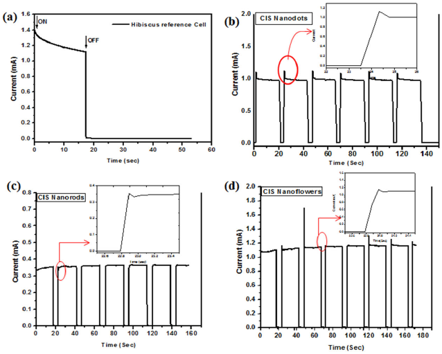
FIGURE 7 Shows the Optical switching of (a) hibiscus-sensitized reference solar cell, (b) hibiscus-sensitized solar cell with CIS Nanodots, (c) hibiscus-sensitized solar cell with CIS Nanorods and (d) hibiscus-sensitized solar cell with CIS nanoflowers.
TABLE I Comparison of the photovoltaic figures of merit for the fabricated CIS-based DSSCs as well as the reference cell
| Hibiscus Reference cell | Hibiscus + CIS Nanodots | Hibiscus + CIS Nanorods | Hibiscus + CIS Nanoflowers | |
| I sc (μA) | 2309 | 1244 | 380 | 1200 |
| V oc (mV) | 480 | 500 | 130 | 460 |
| FF | 0.25 | 0.26 | 0.24 | 0.32 |
| ƞ% | 50 x 10-3 | 35x10-3 | 2.2x10⁻³ | 32x10-3 |
| Settling time (ms) | >17000 | 150 | 48 | 50 |
4. Conclusion
In summary, monodisperse CuInSe2 nanoparticles of different shapes (Dots, Rods, Flowers) have been prepared in oleylamine, and TOP using organometallic pyrolysis method at different reaction temperatures (160, 200, 220∘C) respectively. This approach is based on using (In) and (Cu) salts that dissolve in the capping materials (oleylamine) and react with the Se powder dissolved in trioctylphosphine “Se-TOP complex” at the same time. The particle size and shape of the as-prepared CuInSe2 was measured by the HR-TEM. We successfully prepared CIS quantum dots as small as 3 nm, and we were able to control the morphology and tune it to rods or flowers by increasing the reaction temperature. The crystal lattice structures of the as-prepared CuInSe2 nanoparticles of different shapes were indicated as tetragonal lattice structures using the X-ray diffraction (XRD). The possible growth mechanism to explain the shape control of the CuInSe2 nanoparticles was proposed and discussed via the oriented attachment mechanism.
Also, the effect of the CIS nanoparticles (nanorods, nanodots, and nanoflowers) on enhancing the photocurrent response (optical switching) of the dye-sensitized solar cell was studied. It was found that the CIS nanodots reduce the settling time to 150 milliseconds after it was 17 seconds in case of the Hibiscus sensitized reference solar cell. CIS nanoflowers further reduce the settling time to 50 milliseconds and CIS nanorods gives the smallest settling time of 48 milliseconds. However, incorporating CIS Nanorods leads to very low conversion efficiency. Taking both the conversion efficiency and the photocurrent response into account, we conclude that CIS nanoflowers give the best performance. This is because the nanoflowers are uniformly distributed and highly interconnected throughout the whole sample; this provides a continuous path for the charge carriers between the dye and the back electrode.

