


 text new page (beta)
 English (pdf)
 Article in xml format
 Article references
 Send this article by e-mail
 Cited by SciELO
  Similars in
SciELO
Similars in
SciELO 
 Permalink
1. Introduction
Due to the narrowest bandgap (0.18 eV, at room temperature), the highest electron mobility (78000 cm2V-1s-1) and the largest g factor, indium antimonide (InSb) was widely used to make high-speed devices and infrared (IR) detectors [1]. With the development of nanotechnology, nanostructure of □-V group semiconductors has aroused great interest among scholars [2].One-dimensional nanostructure of InSb was one of the search hotspots. There were many ways to synthesize InSb nanowires. For instance, chemical vapor deposition [3-5], electrochemical deposition [6-7], Chemical beam epitaxy [8]. Most of the methods required metal nanoparticles as catalysts. The growth of InSb nanowires on silicon or other III-V semiconductor substrates have been reported [9-10]. The growth temperature of different substrates are varied greatly, the growth temperature of InSb nanowire on silicon substrates was generally higher than that on other □-V group semiconductors substrates [9-10]. However, □-V group semiconductors substrates is expensive. In this paper, we use a simple process to arrange Au nanoparticles, and the InSb nanowires were successfully grown on silicon wafers by adding gallium.
2. Experimental procedure
We used silicon as a substrate for the growth of InSb nanowires. Firstly, the η-type Si (111) substrate was cleaned by sonicating in acetone and ethanol for 5 min respectively. Then rinsing with deionized water. Secondly, an Au film with 5-10 nm thick was deposited on silicon by magnetron sputtering. Finally, Au islands were obtained through annealing Au film at 700° C for 15 minutes [11]. Figure 1 shows the Au islands.

This is a simple and economical way to arrange gold nanoparticles.
We employed the two-zone CVD system with Mass Flow Controller (MFC). InSb (99.999%, Alfa Aesar) and Ga (99.999%, Alfa Aesar) were used as the source materials, put in a quartz boat. Silicon wafers were located 7 cm downstream from the source materials as shown in Fig. 2.
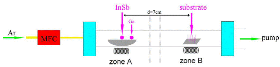
Figure 2 Diagram of tubular furnace, the source material is in the heating center, and the substrate is located 7 cm downstream from the Source material.
Zones A and B rise to 700° C and 510° C respectively in 60 minutes, then the pure argon was introduced as the carrier gas to transport the InSb vapor to the Si substrate. During the whole synthesis process, high-purity Ar (99.99% purity) was used as the carrier gas, the Ar flows at a flow rate of 30 sccm, and the pressure in the tubular furnace was maintained at low pressure (~ 10-4 Torr) by pump for 90 min. After growth, the surface color of the substrate is blue with white. The grown nanowires were analyzed by Scanning Electron Microscope (Zeiss Sigma), field-emission transmission electron microscope with EDS Attachments (JEM-2010 FEF).
3. Results and discussions
Figure 3 shows a SEM image of InSb nanowires with and without gallium. The nanowires had a diameter in the range of 60-100 nm and 1-5 μm in length. The density of nanowires in Fig. 3a is higher than that in Fig. 3b. The results show that the addition of gallium is more conducive to the formation of wire structures.

Due to the incongruent evaporation of III and V elements when InSb was heated [9], the V/III ratio cannot be directly and independently controlled. The V/III precursor ratio supply was unbalanced during the growth [12-13], which is bad to the growth of InSb nanowires by direct evaporation of InSb.
The Au particles show catalytic activity only when they absorb enough indium to form AuIn2 particles, and the temperature is above AuIn2-InSb eutectic temperature [9]. When Au particles absorb indium and show activity, then it will absorb antimony and begin to grow InSb, and the process can be expressed as follows:
AuIn2 + Sb → AuIn + InSb
[14] but the growth of InSb nanowire is limited, due to the imbalance of the residual amount between Sb source and insource. Finally, the Sb element is exhausted, and the growth of InSb nanowire stops. So the length of InSb nanowires is not more than 5 micrometers in our samples shown in Fig. 3a and in other works [4]. As seen from the above results, if we want to grow long InSb nanowires, the supply of Sb element in the late growth stage is very important.
As adding gallium can increase the density of nanowires, we think that gallium was evaporated and coated on the surface of Au catalyst nanoparticles, to form Au-Ga alloys by isothermal solidification in the early stage of growth. Then Indium is easily absorbed by the alloy on the surface of Au particles and then continues to enter the Alloy layer to form Au-In alloy particles, with the continuous absorption of In, Au-In-Ga particles are finally formed which has catalytic activity. The Au-In-Ga particles will absorb Sb for growth. The process is shown in Fig. 4. The melting point of gallium is much lower than that of indium, so gallium is easy to isothermal solidification with gold. Hence, catalyst particles will show activity faster than without gallium. So adding gallium was very helpful to nucleation and growth of InSb nanowire, and so the density of nanowires is increased.
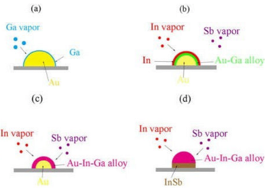
Figure 4 (a) In the early stage of growth, gallium was evaporated and coated on the surface of Au catalyst nanoparticles. (b) Gallium and gold form Au-Ga alloy layer by Isothermal solidification and indium is easily absorbed by the Au-Ga alloy layer. (c) In and Au-Ga alloys continue to form Au-Ga-In alloys by Isothermal solidification and begins to absorb antimony. (d) Indium continues to adsorb, and Au particles completely formed Au-Ga-In alloy particles, nucleate and begin to grow.
The EDS analysis of the catalyst nanoparticle was characterized as shown in Fig. 5b. The Au, In, Sb and Ga elements could be detected in the catalyst particle. The content of gallium in the catalyst particle is low, and the atomic ratio is 1.3% by EDS analysis. Figure 5c is an EDS analysis on the body of the nanowire. Ga is 0.4% in atomic ratio, so it can be considered that gallium did not form a large number of impurities into nanowires. We think that the low content of gallium in the catalyst particle due to the gallium source materials in the quartz boat covered with antimony after gallium evaporates for some time, evaporation was blocked. The O peak is from the outer layer of the InSb nanowires which were quickly oxidized after exposure to the atmosphere.
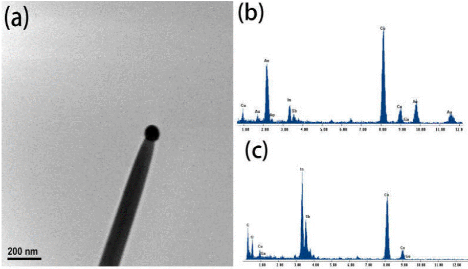
Figure 5 (a) shows a TEM image of the nanowire. As can be seen, there is a catalyst nanoparticle at the tip of the nanowire, which shows spherical morphology. It indicated that the nanowires are grown through the VLS mechanism.
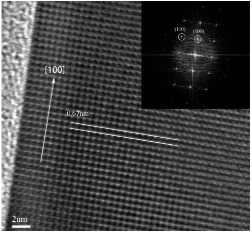
Figure 6 shows an HRTEM image of the single nanowire with the inter-planar distance between the lattice fringes being 0.67 nm which is very close to the lattice constant of 0.648 nm for bulk cubic InSb. Inset is an FFT (fast Fourier transform) image of the nanowire, it reveals that the nanowire grows along the [100] direction. This result shows that the grown nanowires have good crystallinity.
SAED analysis of nanowires was performed and we found that the SAED pattern was correspond to the In2O3 rather than InSb, It contradicts the results of FFT analysis. So we consider that the surface of InSb nanowire was oxidized, and the process is shown in Fig. 7. InSb has a low bonding energy of 1.57 eV and has the largest lattice parameter (0.648 nm) of the group III-V semiconductors, it will dissociate easily at high temperatures, some researchers believe that the InSb keep chemical stability requires temperatures below 400°C [5]. When the tubular furnace naturally cools to room temperature after growth, since our growth temperature is 510°C, the newly grown InSb nanowires will continue to thermal decomposition and the Sb atoms will escape from the of the nanowires, finally, a layer of indium will be formed on the surface of the InSb nanowires. Once the sample was taken out, the nanowire will exposed to air, the In layer will be oxidized to form In2O3 layer by oxygen in the air. The reason for the contradiction between SAED and FFT images was that the penetration depth is different due to the different acceleration voltage of TEM electron beam, In2O3 layer on the surface of the nanowire was detected by SAED and InSb inside the nanowire was detected by HRTEM.
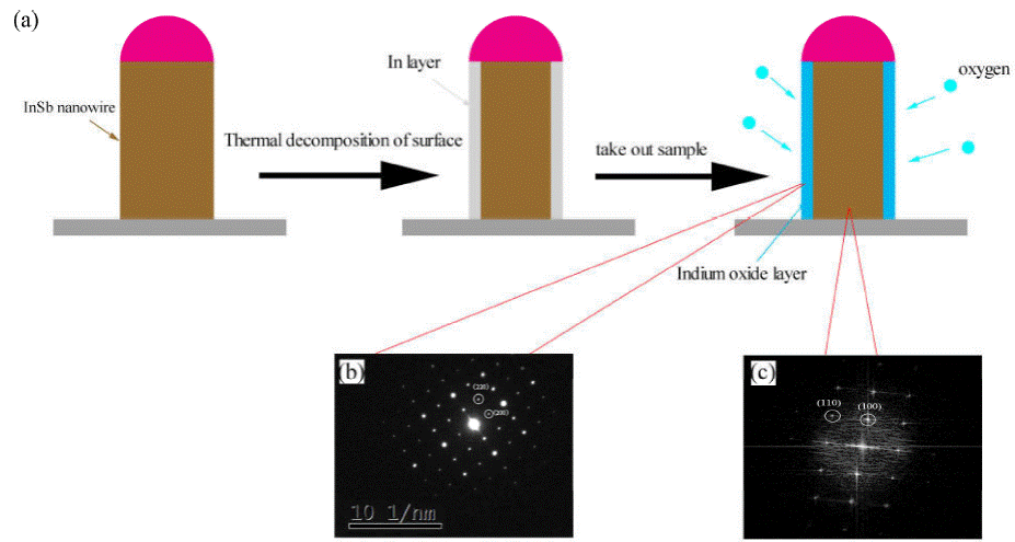
Figure 7 (a) Schematic diagram of surface oxidation process of InSb nanowires. (b) SAED pattern of the nanowire. (c) The FFT image in Fig. 6.
Figure 8 shows nanowires with different morphologies. In Fig. 8a, it could be seen that there were some catalyst spherical particles adhere to nanowires, some on side of the nanowires, and the other at the tip of the nanowire. For the else nanowires, there is no catalyst spherical particle. We think catalyst spherical particles on the side or no catalyst particle on nanowires result from catalyst particles dropping during nanowire growth, which can be demonstrated in the back. Of course, when catalyst particle drops, InSb nanowire growth ceases at once.
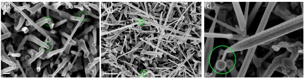
In Fig. 8b, it is interesting to be found that there are double particles at the tip of the nanowire. It is our first time to discover this phenomenon. One of the double particles is Au catalyst particle, the other may be In particle. Owing to the incongruent evaporation of InSb, antimony is consumed and only Indium remained in the later stage of the growth. Indium continues to be absorbed by catalyst particles and no Sb elements, so In ele- ments segregate and In particles are formed.
In Fig. 8c, it can be seen that the Au catalyst particle at the tip of a nanowire would drop out but still connected to the tip. As mentioned above, during the later stage of the growth, antimony is consumed and only Indium has remained, so the Au catalyst particle was connected to InSb nanowire by a very thin in the neck. If the growth process continued, catalyst particle would drop, and InSb nanowire growth would cease. It confirms that no catalyst particle on nanowires would be due to catalyst particles dropping.
4. Conclusion
In this paper, we investigated the effect of Ga on the growth of InSb nanowires. The results show that the density of nanowires can be increased by adding gallium. Moreover, gallium does not enter nanowires in large quantities to form impurities. The nanowires were grown by VLS mechanism used the gold nanoparticles as a catalyst. That gallium coated on the surface of Au catalyst nanoparticles is very helpful to nucleation and growth of InSb nanowire. The grown nanowires were 1-5 μm in length and 60 to 100 nm in diameter. The HRTEM image showed that the grown nanowires had good crystallinity. Because of the incongruent evaporation of InSb, nanowires showed different tip morphologies such as one or double and no nanoparticle on top of nanowires. The phenomenon that catalyst particles dropped out from nanowires was discussed and that accounted for nanowire growth ceasing.

