


 nueva página del texto (beta)
 Inglés (pdf)
 Artículo en XML
 Referencias del artículo
 Enviar artículo por email
 Citado por SciELO
  Similares en
SciELO
Similares en
SciELO 
 Permalink
1. Introduction
Solar cells processed in the technology of thin films in the superstrate configuration have been studied in the last decades. In this configuration, an intermediate layer of a high resistivity material known as high resistive transparent (HRT) layer is usually introduced between a transparent and conductive contact, known as Transparent Conductive Oxide (TCO) and a window material, which is generally the Cadmium sulfide (CdS), in the TCO/HRT/Window structure. The HRT layers have demonstrated to have a very important role in the whole device, like the possibility of depositing CdS films with thicknesses below the 100 nm, with good adhesion and without pinholes, and improve the morphological properties of the TCO, if this presents high roughness and/or pinholes. The use of bilayers TCO/HRT, as frontal contact has become a standard procedure in CdTe solar cells [1-3]. Usually the TCOs and the rest of the films comprising the solar cell are deposited by the same workgroup. However, many other research groups acquire commercial conductive glasses, which are used as TCO. The deposition of an HRT layer onto commercial conducting glass not only can improve the growth conditions of the CdS films, but also can be used to improve the morphology of the TCO layer and reduce the resistance of the frontal contact which directly decreases the series resistance of the solar cells and therefore improves the value of its efficiency. Among the available TCOs, the SnO2:F film seems to be more appropriate for thin film solar cells technology due to its mechanical and chemical stability at high temperature. It is expected that the use of SnO2 as HRT layer will enhance the properties of SnO2:F/CdS, improving the solar cell performance. Recently other type of solar cells based on the Sb2Se3 absorber has attracted increasing attention as a photovoltaic material due to its non-toxic and earth abundant constituents, high absorption coefficient (~ 105 cm -1 ), and suitable band gap (1.2 eV), however the highest efficiency reported in solar cells of Sb2Se3 is about of 7.6%, fabricated in the superstrate configuration [4]. It has been established in several investigations, that there are several aspects that limit obtaining high efficiency solar cells in these compounds. The existence of potential barrier in the front and rear contacts is one of effects that must be over-come. In a previous work, we have reported the decrease in contact resistance from 4.7 Ωcm2 to 0.8 Ωcm2 when was used the TCO/CdS and TCO/HRT(SnO2)/CdS, respectively, through the pre-thermal annealing in Ar atmosphere of TCO, followed by the deposition of the SnO2 layer by pneumatic spray pyrolysis technique with post-thermal annealing in O2 atmosphere, reaching an improvement of the CdTe solar cell conversion efficiency [5]. In this work, expanding previous studies, we present the results about the physical characterization of the TCO/CdS and TCO/HRT/CdS-systems by means of X-ray Photoelectron Spectroscopy, Secondary Ion Mass Spectroscopy, and Transmission Line Method (TLM) techniques, where the SnO2-HRT layer has been deposited by pneumatic spray pyrolysis and magnetron sputtering techniques, with the aim of comparing the influence of these two growth techniques in the improvement of front contact for its further use in the processing of TCO/HRT/CdS/Sb2Se3 solar cells, which, to our knowledge have not been processed with this configuration.
2. Experimental
The schematic structure of the front contact is shown in Fig. 1. T-15 from Pilkington was used as commercial conducting oxide with a SnO2:F layer of 350 nm. SnO2 layer deposition was carried out by Pneumatic Spray Pyrolysis (PSP) technique from the SnCl4*H2O dissolved in a mixture of ethanol and deionized water (1:1). The solution was sprayed onto glass substrates under the following conditions: distance between the nozzle and the sample of 30 cm, air pressure of 40 kPa, 5 mL/min of solution flow and substrate temperature stablished at 570 ° C. Samples were deposited on areas of 6.25 cm2. For this deposition technique, an automatic spray system was used, where the speed of movement of the nozzle can be varied in a range of 4-30 cm/min. For the deposition of SnO2 thin films via RF magnetron sputtering, the pure SnO2 target was used and the substrate-to-target distance was 30 cm. The chamber of magnetron sputtering was evacuated to a base pressure of 1×10⁻³ Pa before the deposition. The sputtering power under Ar atmosphere was 80 W, the deposition time of 50 minutes and the working pressure of 2.7 Pa were maintained constant for all depositions. The commercial conducting glasses T-15 (15 Ω/sq) were previously thermally treated in Ar atmosphere during 30 minutes at 500 ° C and after this procedure the HRT-SnO2 layers (with thicknesses approximately 17 and 70 nm) were deposited onto TCO by the two mentioned techniques, which were submitted to a post thermal-treatment at 400 ° C during 45 minutes under O2 atmosphere. Finally, a thin-film layer of CdS of 100 nm was deposited by the CBD technique on the TCO, and the bilayers TCO/HRT. X-ray photoelectron spectroscopy (XPS) analysis was carried out using a SPECS spectrometer with a Phoibos 100 1D DLD using a monochromatic X-ray radiation Al Kα. The elemental bulk-distribution was analyzed using the XPS technique combined with Ar+ depth profile sputtering through a 5000 eV of Ion bombardment. All the reported binding energy data have been calibrated using the residual carbon present on the surface of SnO2 thin films, positioned at 285.0 eV. The analysis of XPS data was performed using the casa XPS software.
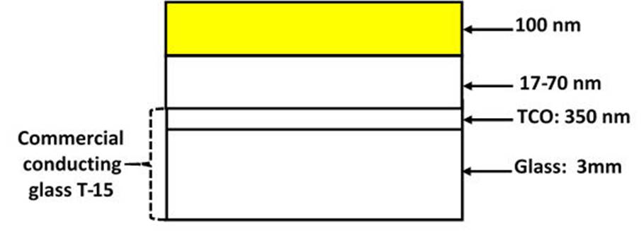
Figure 1 Schematics of a T-15/SnO2/CdS front contact. Typical thickness values for each layer are shown in this figure (not to scale).
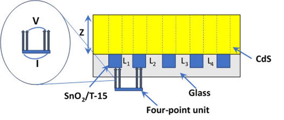
Semi-quantitative secondary ion mass spectroscopy (SIMS) depth profiling was made on T-15/HRT and T-15/HRT/CdS structures using a TOF-SIMS-5 secondary ion mass spectrometer from ION-TOF GmbH. We used a double beam analysis regime: a focused cesium ion beam with an energy of 500 eV and ion current of 60 nA was raster scanned over 500 × 500 μm2 area; Then a pulsed Bi+ ion beam was used to analyze a 150 × 150 μm2 central area of the sputter crater. Secondary CsM+ cluster ions (where M is an element of interest) were monitored in order to minimize the SIMS matrix effect. Contact resistance measurements were carried out by means of the four-point-probe method, using a Lucas Pro-4 Resistivity Measurements System, in order to minimize the effects of electrodes resistance. The contact resistance is one of the parameters of greatest weight in the value of the series resistance of a solar cell. In the case of solar cells with superstrate structure, the series resistance of the device is directly influenced by the front and rear contacts. Accurately measuring of the contact resistance is therefore very important. The most common method used to calculate the contact resistance of solar cells is the transmission line method (TLM) [6-8]. Briefly the method consists in the measuring of the total resistance between two contacts with length Z and plotted as a function of contact spacing L.
The total resistance, R T , between two adjacent contacts is:
From Pouillet’s law the resistivity of the semiconductor is given by:
Where d is the semiconductor thickness.
If we denote by ρ c = R c A c as specific contact resistance with A c the contact area and R c the contact resistance then R c = ρ c =A c
In these calculations it should be considered that the current does not flow uniformly in the contact and therefore is necessary to consider the physical length (L T ) and width of the contact (Z) to determine the real contact area where the current flows and the effective area of the contact can be considered as L T Z.
Therefore
R c can be deduced according to the potential distribution underneath the contact and is represented by:
If it is assumed thatZ > 1:5L T , then R c can be written as:
The transfer length L T is the average distance that an electron (or hole) travels in the semiconductor beneath the contact where AC is the area of the contact. LT is defined as:
Finally, the Eq. (1) can be written as:
In case of high value of ρ is necessary to choose small values of L (on the order of μm) to reduce the influence of semiconductor resistance on the R T values. To achieve the above, the structures are usually manufactured using photolithography, which is a complicated step. For this reason, we have proposed a new alternative, which consists of the use laser scriber to establish the distance between contacts that comply with the condition that their separation must be of the order of micrometers. Furthermore, the four-point probe was the method used for the measurements of the specific contact resistance, because this method eliminates the influence of other contacts in the structure to be studied. Figure 2 shows a schematic view for the measurements of the contact resistance by the TLM method. The contribution of each resistance is defined as follows: R p referred to the tip, the contact-resistance between the tip and the bi-layers (SnO2/T15) is represented by R tip-bilayers, the semiconductor resistance by R sc and the bi-layers-semiconductor contact resistance by R bi-layers/CdS. In the four-point method the R tip-bilayers is canceled and R p is negligible with respect to R sc therefore, the total resistance R T is reduced to:
where V is the voltage reading of the voltmeter and I is the current carried by the two current carrying tips. The following structures were studied: T-15/CdS and T-15/PSP-SnO2/CdS, with two thickness of the SnO2 (17 and 70 nm). Prior the deposition of CdS thin films, the contacts were isolated by laser scribing technique. Details about the laser characteristics and the experimental setup to perform the laser scribing were described in Ref. [7]. The test structure was made with parallel and planar contacts with separation between then from 20 to 102 μm. Since the CdS film covers the entire area during deposition, the laser scribing system also was optimized to remove a CdS zone to be able to place measurement pins on the contacts without damaged the T-15-SnO2 structure.
3. Results and discussions
Figure 3 shows the XPS analysis for the studied samples. Two components corresponding to O-Sn4+ and a small component of BE at about 532.4 eV have been distinguished, respectively. The contribution located at ~ 532.4 eV is not clear yet and has been related to the chemisorbed oxygen Species [9-13]. Furthermore, is important to note that the O1s XPS spectra show the formation of a SnO2 buffer layer independent of the deposition technique. The deconvolution of high-resolution O1s XPS spectra for the samples prepared by PSP and Sputtering is shown. Upon analysis, it is observed that the peak position of sample deposited by the PSP is closer to the O-Sn4+ value (530.5 eV) taken from the National Institute of Standards and Technology (NIST) database [9] in comparison to sample deposited by Sputtering. In addition, from the sample deposited by Sputtering is observed a reduction of undesired chemisorbed oxygen contribution with a relation area O-Sn4+/OChem of 4.7, respect the value 3.6 in the case of the sample deposited by PSP. Therefore, even when the Sputtering deposition produces low chemisorbed contribution due to high quality and vacuum condition, the pneumatic spray pyrolysis deposition achieve a buffer layer with a more intensive contribution of O-Sn4+ and a closer peak position to the Ref. [6] than the deposited by Sputtering. We explain this result taking into account that pneumatic spray pyrolysis deposition of the SnO2 layer was carried out in a rich Oxygen atmosphere (air) while in the Sputtering deposition the Oxygen source arises from the SnO2 target stoichiometry. To study the additional possible contributions, the full width at high maximum (FWHM) of the O-Sn4+ contribution is illustrated in Table I, where it is clearly observed that the studied samples are closer to the database reference and Sputtering deposition performed the lowest (FWHM) sample as is expected by high vacuum deposition. Furthermore, the same analysis was performed for the Sn 3d 5/2 component revealing good quality samples in comparison to samples deposited by L-CVD of reference [12]. Finally, we have investigated the electrical behavior and the band gap alignment for heterojunctions solar cells. The Fig. 4 shows the Valence band analysis of the studied samples extracting the energy difference between Fermi level and valence band maximum by the well know method of extrapolation slop of the first valence band ejected photoelectrons to the y-axis according to Ref. [11] where the Fermi level is taken at cero eV. Then, the analysis revealed n-type nature for HRT layers deposited by the Sputtering and high resistivity closer to intrinsic level for pneumatic spray pyrolysis deposition. To understand with more detail the conductivity nature the stoichiometry was quantified in every sample by XPS and the results are shown in Table II. From the Table II is observed that better [O]/[Sn] relation is obtained by pneumatic spray pyrolysis closer to 2 (1.91) in comparison to the Sputtering with a relation of 1.66 revealing an Oxygen deficit. These results ratify the best stoichiometry for the sample deposited by PSP with respect to that deposited by Sputtering, which means a better HRT condition for the PSP layer. Secondary ion mass spectrometry is a powerful technique that allows studying the interdiffusion between the different constituent layers of a solar cell and therefore understand and improve aspects that affect the formation of a good diode, among which stand out the front and rear contacts. It is especially important in the case of multi-layer analysis where inter-diffusion from layer to layer can take place with the possibility of analysis of all elements from hydrogen to uranium.
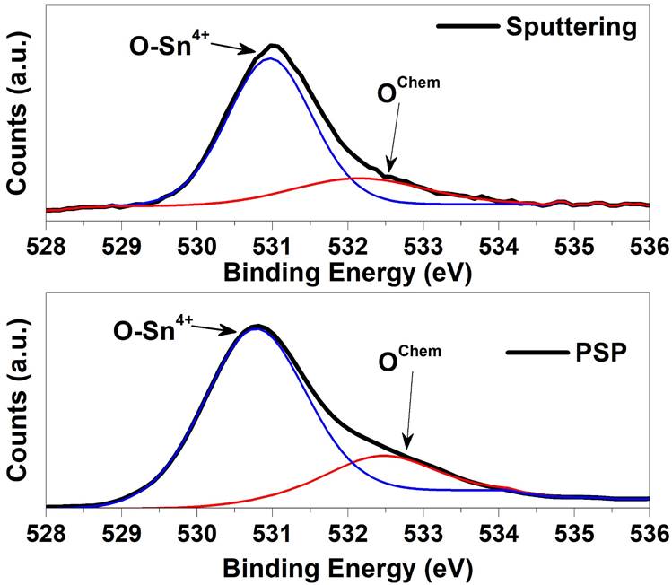
Figure 3 O1s XPS spectra of the HRT- SnO2 layer deposited by PSP and sputtering. The deconvolution of high-resolution O1s XPS spectra for the studied samples is shown also.
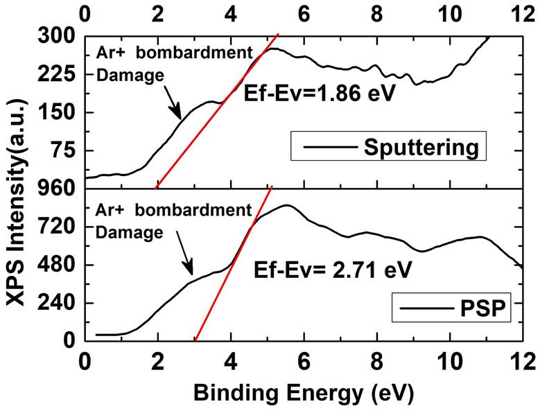
Table I O-Sn4+ and Sn 3d5/2 FWHM of the SnO2-PSP and SnO2-Sputtering samples and the comparison with the references.
Table II SnO2-Sputtering samples and the comparison with the references.
| Sample | PSP | Sputtering |
|---|---|---|
| Sn 3d Peak (eV) | 487.0 | 487.1 |
| O1s Peak (eV) | 530.90 | 530.96 |
| Sn FWHM (eV) | 1.38 | 1.43 |
| Sn FWHM (eV) | 1.43 | 1.31 |
| Sn 3d (%) | 34.4 | 37.64 |
| O1s (%) | 65.6 | 62.35 |
| [O]/[Sn] ratio | 1.91 | 1.66 |
| E f -E v (eV) | 2.71 | 1.86 |
Figure 5 shows the SIMS depth profile for a TCO/SnO 2 structure where the SnO2 thin films were deposited by PSP (a) and sputtering (b). For the PSP and sputtering the profiles are similar in both cases: high concentration of O and Sn and and diffusion of F towards the SnO2 however, the minimum concentration of F in the deposit by PSP is 1020 cm -3 at 15 nm and in the case of sputtering it is 1019 cm-3 at 41 nm, which means that the F diffuses more in the films deposited by PSP, probably because in the first case the deposit is made at 570 ° C while in the case of sputtering the substrate is not heated. Impurities of C, Cl and Na appear in both profiles. In Fig. 6 the SIMS depth profile are shown, when the HRT layer deposited by PSP and Sputtering is added between the T15 and CdS. In the CdS layers high concentrations of Sn and O are observed (~ 1022 cm -3 ) and the F concentration reaches a value of 1021 cm-3. Cl, Na and C are also detected with relatively high concentrations. Carbon is a source of contamination that usually appears due to the samples manipulation, the sodium comes from the glass substrate and the chlorine from the salt used in the spray pyrolysis. The comparison between Figs. 5 and 6 clearly shows that the thickness of HRT-SnO2 deposited by both methods is insufficient to guarantee the decreasing of interdiffusion between the TCO/SnO2 and the CdS, consequently the HRT layer will influence the properties of the window material and finally the properties of the solar cell. Taking into account the results of the SnO2 layer deposited by PSP with respect to the deposited by sputtering, the thickness of the HTR layer deposited by PSP was increased to 70 nm, followed by a CdS layer of 100 nm. Figure 7 shows the comparison of the SIMS depth profiles with the thicknesses of SnO2 buffer layers of 17 and 70 nm. At 70 nm thickness, the atomic concentrations of fluorine, tin, chlorine and sodium decreased by a factor of 1700, 100, 1000 and 2000, respectively, showing the effect of the SnO2 thickness on the attenuation of the diffusion of these atoms in the CdS window layer.
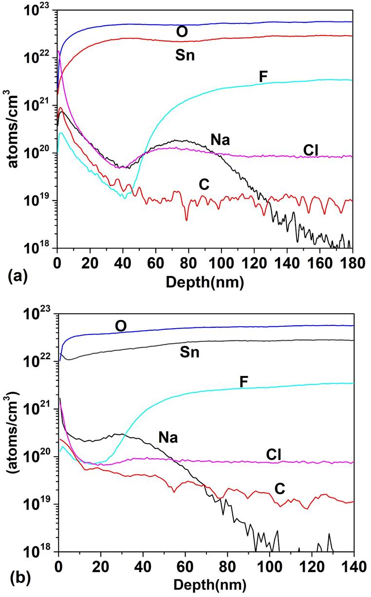
Figure 5 SIMS depth profile of TCO/SnO2 structure: (a) atomic concentration as a function of depth for SnO2 deposited by PSP and (b) atomic concentration as a function of depth for SnO2 deposited by Sputtering.
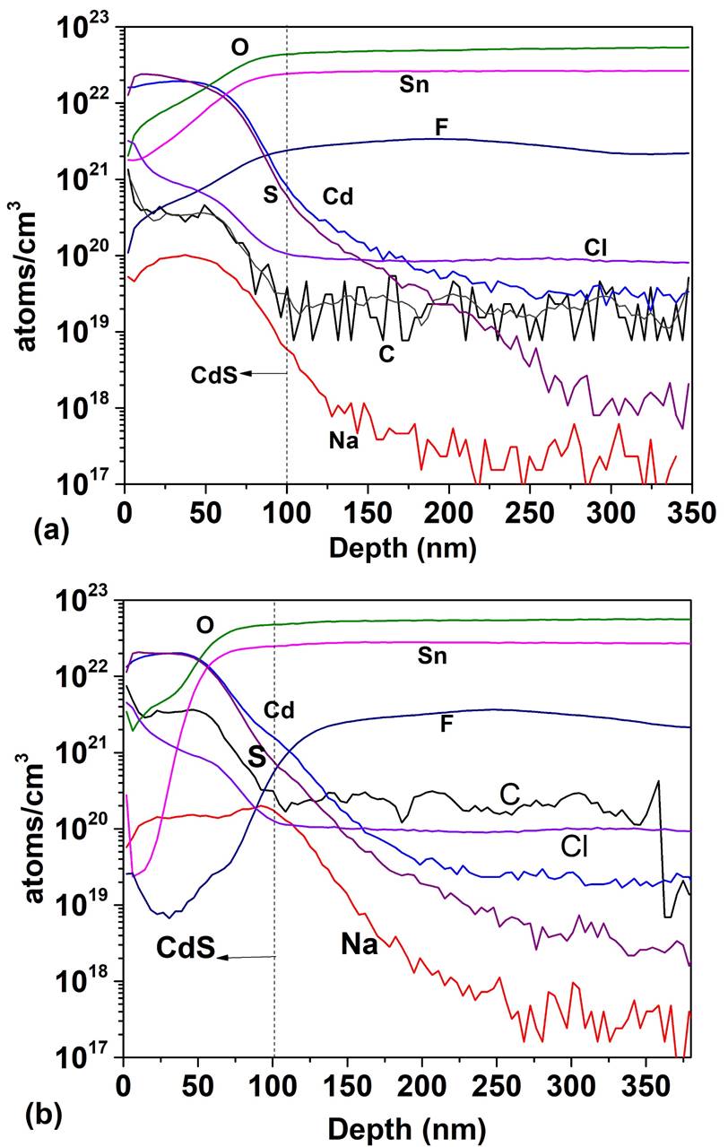
Figure 6 SIMS depth profile of TCO/SnO2/CdS structure: (a) atomic concentration as a function of depth for SnO2 deposited by PSP and (b) atomic concentration as a function of depth for SnO2 deposited by Sputtering.
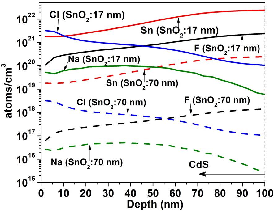
Figure 7 Effect of the increase the thickness of the SnO2 layer deposited by PSP on the concentrations of the diffused atoms of F, Sn, Cl and Na towards the window layer of CdS.
In order to study the influence of the different configuration on the contact resistance the TLM method was applied. Figure 8 shows the total resistance dependence on the contact spacing for three structures, fabricated through the deposition of SnO2 buffer layer by PSP. The specific contact resistance calculated value for each structure is also displayed in the inset of Fig. 8. As can be observed the lowest value of the specific contact resistance is obtained for the structure with the buffer layer of 17 nm of thickness. The increase in the thickness of the SnO2 layer leads to an increase in the contact resistance, which is still lower than the resistance in the case of deposits of the CdS directly on the T15. From these results it is observed that the thickness of the buffer layer is a critical parameter in the contact optimization. By increasing the thickness, it is possible to reduce the interdiffusion of the atomic species, but at the expense of an increase in contact resistance. The highest power reported conversion efficiency of Sb2Se3 thin film solar cells with a ZnO/Sb2Se3 superstrate is 5.93%, where the ZnO was deposited by PSP [14], so a study similar to that presented in this work is in process.

4. Conclusions
In conclusion, XPS measurements show that more resistive layer is obtained by PSP, while better crystalline quality is observed for the sample deposited by sputtering. Inter-diffusion between CdS and T-15/SnO2 determine high concentration of Sn, F and O and contamination of C, Cl and Na in the CdS layer, due to the thickness of SnO2 about 17 nm. An increase in the thickness of the SnO2 layer decreases the diffusion of these elements but the contact resistance is increased, which means a compromise between the contribution of the resistance of the HRT layer to the series resistance of the device and the capacity of that layer to attenuate the diffusion of atoms to or from the CdS. It is necessary to clarify that the controlled introduction of alkaline elements in the CdS buffer layer, has demonstrated an improvement of the efficiency of the solar cells of CZTSe and CuInGaSe compounds, therefore, a further study of the influence of the interdiffusion of the atoms on the properties of the different solar cells, processed in the superstrate configuration using different HRT layers deposited by PSP, will be necessary. According to the results presented in this work, the optimization of the thickness of different HTR layers in new solar in superstrate structure is in progress.

