


 nueva página del texto (beta)
 Inglés (pdf)
 Artículo en XML
 Referencias del artículo
 Enviar artículo por email
 Citado por SciELO
  Similares en
SciELO
Similares en
SciELO 
 Permalink
1. Introduction
Metal oxide nanostructures are of considerable interest due to their properties like a high volume-area ratio which is a very important property of nanoscale [1]. Likewise a new family of structures has been developed, named for what they look like, e.g. nanosheets, nanograss, nanoribs, nanorods, nanopores, nanowires, nanobelts and so on [2]. Within this family, there is one special type of nanostructure which has, in fact, a double surface area that offers one direct and efficient pathway for electron transport [3] and more available area for nanoparticles insertion [4], they are called nanotubes [5].
Titania nanotubes (TNT) can be synthesized using the anodic oxidation process, more generally called anodization, first reported in 2001 for titanium dioxide [6]. This versatile technique uses titanium (anode) and, commonly, a plate, rod or foil of pure platinum as cathode [7], this material is too expensive. In the initial stages of the anodization process, field-assisted dissolution dominates chemical dissolution due to the relatively large electric field across the thin oxide layer [8]. Small pits formed due to the localized dissolution of the oxide, act as pore-forming centers, after which these pits convert into pores with increasing pore density, uniformly, over the surface. The pore growth occurs due to the inward movement of the oxide layer at the pore bottom (barrier layer) [9]. The rate of oxide growth at the metal/oxide interface and the rate of oxide dissolution at the pore-bottom/electrolyte interface ultimately become equal, thereafter the thickness of the barrier layer remains unchanged although it moves further into the metal increasing the pore depth. The formation of small pits in the inter-pore regions, eventually leads to pore-separation and tube formation. The thickness of the tubular structure ceases to increase when the chemical dissolution rate of the oxide at the mouth of the tube (nanotube array surface) becomes equal to the rate of inward movement of the metal/oxide boundary at the base of the tube [10].
TNT’s with smooth tube walls could be synthesized by adjusting the water content in the organic electrolyte (ethylene glycol). An interesting observation of anodization using an ethylene glycol electrolyte is that the as-anodized TiO2 nanotube arrays are covered by a surface layer. This surface layer is composed of nanotubes with a diameter of only a few nanometers, and has been called nanograss [11]. Particularly long TNT’s have to be grown by extended anodizing time. Often a disintegration of the top end of nanotubes due to chemical dissolution is observed, and then the ordered TNT’s transform into TiO2 nanowires or nanograss [12,13]. The as-anodized oxide layer formed is amorphous in nature [14]. Generally, crystallization is achieved through thermal treatment at 300-500 ° C [15] in a variety of atmospheres for high-performance applications with anatase phase [16].
Results of previous investigations, focused on TiO2 nanotubes obtained by anodization using an NH4F salt concentration from 0.3-0.5 wt %, presents information about how voltage and time affect to nanotubes morphology. These results are valid for low concentration. Moreover, with this range the anodization usually takes hours. It is known that increasing salt concentration, the electrolyte increases their conductivity and the anodization speed (oxidation-dissolution) suffer also an increment.
The main goal of this study is to identify how time and voltage is implicated on the morphology of nanostructures of TiO2 for a specifically NH4F salt concentration 1.2 wt %, taking advantage of this percent and remarking the great importance of the oxide growth-dissolution speed with this electrolyte concentration. A good tube shape, a vertical alignment, and a free top layer are necessary characteristics for a better performance in almost all applications. However, the presence of nanograss is so useful to capture nanoparticles (Au-Ag-Cu), for example in SERS applications, and it is why we focus attention to identify it in time and voltage also. Moreover, an important factor in this study was the selection and use of graphite as an effective alternative cathode, due to low cost and optimal nanotube morphology [17-19].
2. Methods
Titanium foils (15 x 15 x 0:1 mm) were first used as an anodic electrode, while pure graphite rods (35 x 6 mm) were used as a cathodic electrode. Titanium foils were cleaned by ultra-sonication successively in ethanol, deionized water, and acetone.
The distance between electrodes was constant in every experiment (30 mm). The foils were anodized in the organic electrolyte: ethylene glycol, 2 % deionized water and 1.2 wt% NH4F; using two electrode configurations.
The anodization was carried out using a DC power source under voltage from 5 to 30 V for a time period from 1 to 6 hours, a constant potential of 30 V for a time lapse from 10 to 360 minutes and another constant potential of 30 V for a time period from 5 to 480 seconds.
After the anodization process, the whole set of anodized samples was rinsed in deionized water, dried and then annealed at 400 ° C for 3 hours. Additionally, there were anodized three samples with 0.3 wt% and 0.6 wt% NH4F for comparison purpose about the velocity of oxidation-dissolution with two constant parameters: 30 V and 1 hour of anodization time.
The morphology and structure of TiO2 were characterized by the Field Emission Scanning Electron Microscope (SEM JSM-7600F, JEOL) according to 5’000, 10’000, 30’000, 50’000 and 100’000 x, 5 kV and 15 kV acceleration voltage, work distance (WD) of 4.9 mm and a SEI-SEM detector, a with size probe current of 5.
Raman spectra were obtained using a DXR Raman Microscope (Thermo Scientific), with parameters: 532 nm green laser, 5x and x objective, 10 mW power, 50 μm slit, 50 samples collection and 3 s time collection. Table I summarizes our experimental parameters and samples name used.
Table I Variable voltage for a time period from 1 to 6 hours (ME group, blue background), constant voltage (30 V) for a time period from: 10 to 360 minutes (MO group, yellow background), 5 to 480 seconds (MI group, green background).
| Sample | Voltage | Time (h) | Sample | Voltage | Time (h) | Sample | Voltage | Time (h) | Sample | Time (min) | Sample | Time (sec) |
|---|---|---|---|---|---|---|---|---|---|---|---|---|
| ME01 | 5 | 1 | ME13 | 15 | 1 | ME25 | 25 | 1 | MO01 | 10 | MI01 | 5 |
| ME02 | 5 | 2 | ME14 | 15 | 2 | ME26 | 25 | 2 | MO02 | 20 | MI02 | 10 |
| ME03 | 5 | 3 | ME15 | 15 | 3 | ME27 | 25 | 3 | MO03 | 30 | MI03 | 15 |
| ME04 | 5 | 4 | ME16 | 15 | 4 | ME28 | 25 | 4 | MO04 | 40 | MI04 | 30 |
| ME05 | 5 | 5 | ME17 | 15 | 5 | ME29 | 25 | 5 | MO05 | 50 | MI05 | 60 |
| ME06 | 5 | 6 | ME18 | 15 | 6 | ME30 | 25 | 6 | MO06 | 60 | MI06 | 120 |
| ME07 | 10 | 1 | ME19 | 20 | 1 | ME31 | 30 | 1 | MO07 | 120 | MI07 | 180 |
| ME08 | 10 | 2 | ME20 | 20 | 2 | ME32 | 30 | 2 | MO08 | 180 | MI08 | 240 |
| ME09 | 10 | 3 | ME21 | 20 | 3 | ME33 | 30 | 3 | MO09 | 240 | MI09 | 300 |
| ME10 | 10 | 4 | ME22 | 20 | 4 | ME34 | 30 | 4 | MO10 | 300 | MI10 | 360 |
| ME11 | 10 | 5 | ME23 | 20 | 5 | ME35 | 30 | 5 | MO11 | 360 | MI11 | 420 |
| ME12 | 10 | 6 | ME24 | 20 | 6 | ME36 | 30 | 6 | MI12 | 480 |
3. Results and discussions
Through Raman spectra, it is possible to confirm the change from an amorphous state to anatase phase, as a result of the annealing process. As per literature reports, the tetragonal structure of anatase belongs to the space group
Generally, all these six Raman modes suffer a shift to red or blue depending on stress, but mainly the E g (v6) mode has a strong relationship with this factor. Alhomoudi et al., explained this relation between E g shift, the Raman intensity and oxide thickness. Trough an experimental and analytical study, it has been demonstrated that when thickness increases, the decreasing of E g shift exists, until the standard position (144 cm -1 ) and this E g shift is due to the stress between substrate and oxide layer [22]. A similar behavior has been related to the confinement effects in nanostructured anatase crystallites [23-26]. Moreover, it has been demonstrated that other factors influencing the position of Raman peaks of nanostructured TiO2 are stoichiometry defects [27, 28]. The three-high wave-number modes 400 cm -1 B 1g , 515 cm -1 A 1g , and 640 cm -1 E g (v1) modes have similarity in Raman shifts, where the modes reduce their shifting from a lower wave number to a higher wave number.
Figure 1 presents the result of increasing the salt concentration where the electrolyte increases their conductivity and the anodization speed (oxidation-dissolution) suffers also an increment. We set 1 hour of anodization time in each case for comparative purpose with 0.3 wt % (A) where there is just a layer of nanosponge [6], 0.6 wt % (B) where it is possible to observe a good shape nanotube layer, finally, 1.2 wt % (C) with the same nanotube layer but with a nanograss structure on the top. This fact is important to remark because that means at the same time we have a fibered structure or in other words, in less time we have the same nanotube layer.
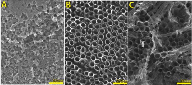
Figure 1 SEM images with a comparison between different NH4F concentrations, as in experimental section (methods) it is expressed: 0.3 wt % (A), 0.6 wt % (B) and 1.2 wt % (C), for a constant potential of 30 V and 1 hour of anodization time.
Figure 2 shows us a Raman spectra comparison between Titanium foil (red line) and an early anodization time of 5 seconds, 60 seconds and 120 seconds of this process. It is an important transition from a very thin film oxide, proper of an initial oxide layer (green line) and a porous oxide layer (blue line). Moreover, 1-2-3 (same figure) shows a schematic draw about the oxide growth process.
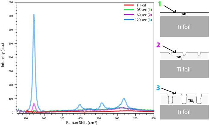
Figure 2 In the initial anodization stage there is a thin oxide film due to the interaction of the metal with O 2- or OH - ions (Raman green line and 1). After these, anions migrate through the oxide layer reaching the metal/oxide interface where they react with the metal and small pits are formed (Raman purple line and 2) acting as pore-forming centers (Raman blue line and 3).
In the initial anodization seconds, there is just a very thin oxide film pore-free due to the interaction of the metal with O 2- or OH - ions (1). As the time increase, after the formation of an initial oxide layer, these anions migrate through the oxide layer reaching the metal/oxide interface where they react with the metal and small pits are formed (2) acting as pore-forming centers. After, these pits will transform into pores with increasing pore density, uniformly, over the surface.
This scheme and Raman spectra from this figure has a strong co-dependency with Fig. 3, where Raman intensity (red dots) and pore diameter (green dots) are introduced as a time function. For a time lapse from 5 seconds to 480 seconds, and with great certainty is clearly visible these dependency. It means a very fast growth (of the oxide) at the initial stage where the titanium foil has a high conductivity but as time increases (and the oxide growth) this conductivity becomes very low (never fall to zero) due the rate of oxide growth at the metal/oxide interface and the rate of oxide dissolution at the pore-bottom/electrolyte interface (blue solid line).
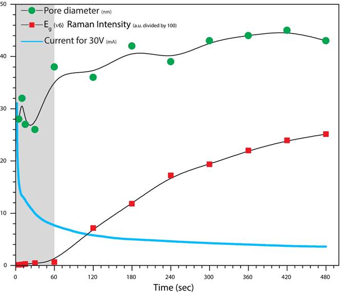
Figure 3 Pore diameter and E g (v6) Raman intensity are showed as a time function. It can be compared with the quick decrease of the titanium foil conductivity. It has been indicated with grey color at the background the first stage of anodization where it is possible to observe a very strong increase for Raman intensity- Pore diameter versus a very fast decrement in current flow.
As an extension of this explanation, it is important to be clear about minimal differences between Ti foil spectra and 5 seconds. Due to Raman spectroscopy is proper to covalent bonding and the Raman laser has a depth of penetration (which depends on the absorption coefficient of the material analyzed), laser wavelength and spot size, these related parameters can explain this similar behavior between spectra. In other words, being a very thin TiO2 film, there is a very low volume of oxide material and it is not possible to observe an important difference, compared with more anodization time (more oxide volume and thickness).
Using Fig. 4 as a descriptive transition from 5 seconds to 8 minutes under constant voltage (30 V), it is possible to explain the oxide growth-dissolution as follows: from titania thin film (A) to random and full presence of pits (B), after a few seconds starts to appear the nanopores (C-K) and finally these pores are transformed to nanosponges (L).
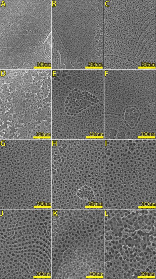
Figure 4 Scanning electron microscopy (SEM) micrographs of TiO2 nanopores layers by anodization under constant voltage (30 V) in ethylene glycol, D.I. water, and NH4F. Anodization time in seconds: 5 (A), 10 (B), 15 (C), 30 (D), 60 (E), 120 (F), 180 (G), 240 (H), 300 (I), 360 (J), 420 (K) and 480 (L). There is a clear evolution or progress about the pore diameter which is also related to oxide thickness and Raman Intensity.
Table II Theoretical Raman shift (cm -1), wavelength (nm), energy and their assignment for anatase phase vibrational modes. Information about the Raman laser is included, where it is possible to observe in an adequate way how the Raman laser energy suffers a little change according to each vibrational mode.
| Raman Shift | Wavelength | Energy | Assignment | |
|---|---|---|---|---|
| (cm-1) | (nm) | (eV) | ||
| v1 | 640 | 550.75 | 2.2514 | E g |
| v2 | 519 | 547.11 | 2.2664 | B 1g |
| v3 | 515 | 546.99 | 2.2669 | A 1g |
| v4 | 400 | 543.57 | 2.2812 | B 1g |
| v5 | 197 | 537.63 | 2.3064 | E g |
| v6 | 144 | 536.11 | 2.3129 | E g |
| Raman laser | 0 | 532 | 2.3308 | - |
According to Fig. 5, it is possible to observe how the Raman intensity (for all vibrational modes) suffers an increment due to oxide thickness, which is progressive as time increases. Similar behavior has been observed in MI group.
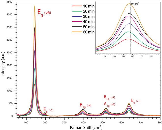
Figura 5 Raman spectra for a time lapse from 10 to 60 minutes of anodization process. There is possible to observe how the whole Raman spectra intensity suffers an increment as a time function. Inside the box there is a partial Raman spectra section where is clearly to appreciate the Raman spectra shift suffered by Eg(v6) mode: 144 cm -1 .
We can fix our attention about the small change in E g (v6) peak position, from a theoretical Raman shift 144 cm -1 position and if this result is compared with SEM micrographs (Fig. 7A), we observe how this vibrational mode appears with a displacement of 3.20124 cm -1 , for an anodization time of 10 minutes, and there exist just a vertically oriented nanotubes layer, which is very thin after all with a tube length of 335 nm; 20-30 minutes attend to relax this stress but 40-50 minutes exhibit a new increment and we can associate it with the presence of nanotube islands and nanograss (Fig. 7D and E).
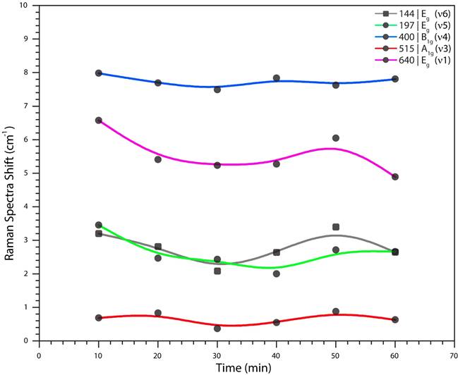
Figura 6 Raman spectra shift behavior of the modes E g (v6): 144 cm -1 , E g (v5): 197 cm -1 and B 1g (v4): 400 cm -1 , (bending type vibrations) and the modes A 1g (v3): 515 cm -1 and E g (v1): 640 cm -1 (stretching type vibrations).
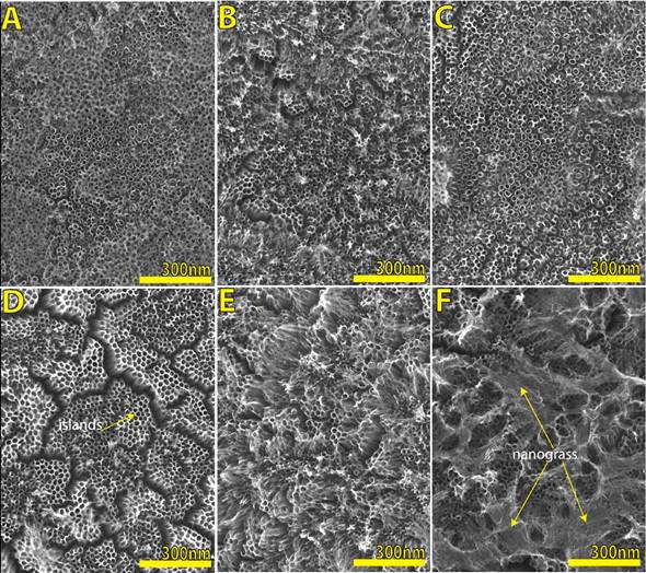
Figura 7 Scanning electron microscopy (SEM) micrographs of TiO2 nanotube layers by anodization under constant voltage (30 V) in ethylene glycol, D.I. water, and NH4F, after the annealing process. Anodization time of A)10 min, B) 20 min, C) 30 min, D) 40 min, E) 50 min, F) 60 min. The nanograss presence is indicated here.
The dominant 144 cm -1 E g (v6) mode is shifted towards a lower frequency by an amount that depends on the thickness of the film (this mode has a strong relationship with this factor). The compressive stresses gradually increase with lower film thickness, which means that the stress gets higher closer to the film and substrate interface (Fig. 5-inset).
The shifts of the 400 cm -1 B 1g (v4) and 640 cm -1 E g (v1) modes were toward lower wavenumbers and decrease with film thickness, but here it is proper to explain that these changes can be mainly attributed to the stoichiometry defects due to the electrolyte age. The literature reports an optimal electrolyte age and a stoichiometry defects study, which is focused on the variating of the H2O percent [29-32], explains how this variation influence on the stoichiometric defects and in consequence affects to the Raman shift. In fact, as the electrolyte is used (increasing the using age), the oxygen will be each time less and less due to the oxide forming.
Figure 6 shows each displacement suffered in the five vibrational modes, as an important fact, two E g modes (v1-v6) have a strong similar behavior due to the displacement of the atoms. For v1, the displacement is produced by oxygen stretching the molecule, and on the other hand, v6 is mainly produced by titanium bending the molecule. These difference are attributed, in the proper calculus, to stretching-bending forces constant of anatase, distance between atoms and ionic radius [20]. In the same way, we can explain the almost similar behavior for v5 vibrational mode but there exists a combinational move of titanium and oxygen bending the molecule.
Figure 7 remarks how TiO2 nanotubes suffer a degeneration: A-B-C shows a good nanotube layer with a very little presence of residual thin oxide layer, it is formed in the first stage of growth [33] for a time of 10, 20 and 30 minutes respectively, even this oxide layer can be easily removed when it is rinsed in D.I. water thoroughly. Here the nanotube diameter is around 52-53 nanometers, which is a good size for insertion of nanoparticles, for example, so it is very important to remark this time lapse where it is possible to have a good shape of tubes; D) This micrograph demonstrates how the nanotubes start to collapse, forming clusters of bundled nanotubes (also called islands), this is due to the surface stress originating during the formation of the oxide films [34] and an irregular topology of substrate; E) here it is very clear to see how the nanotubes are collapsed due to being grown by extended anodizing time, often a disintegration of the top end of nanotubes due to chemical dissolution is observed, and then the nanotubes transform into TiO2 nanograss [35,36]; F) It clearly shows a full presence of well-formed nanograss.
In this study, we use a combined graphic (Fig. 8) in order to do a possible an effective comparison and with it to appreciate the ascendant behavior as an anodization time function for the nanotube diameter, the nanotube length, which has a very strong relationship with Raman intensity. But in this case, we use for comparison, just the E g (v6).
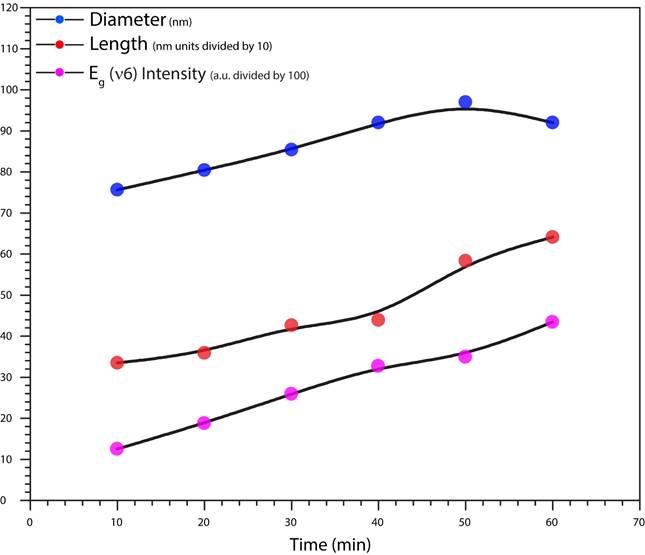
Figure 8 Through a three lines graphic: Red dots for tube length (nm), blue dots for tube diameter (nm) and purple dots for E g (v6) Raman intensity (in arbitrary units scale divided by 100 for comparative purposes), it is easy to compare-deduce and confirm how the behaviors of these three different parameters have a very similar increase moreover they have a strong time dependence linked to Raman shift-Anodization time and oxide thickness.
The ME group has the particular characteristic of being a 6 x 6 samples matrix (6 voltages and 6 different time lapses) and in accord to what we presented before, using 36 samples, it is presented all the behaviors recognized in this study, for diameter and length, as time function, voltage function and even in one case, it is compared diameter-length as function of E g (v6) Raman Shift.
It is important to emphasize the fact that in Fig. 9 there is clearly a marked decrease in the growth rate of the tubes, this reduction in the rate of growth of the oxide in the range of 15 and 20 volts depends on the speed of solution, which in this potential and for the concentration of NH4F used in our research, the dissolution is faster than at lower voltages, so that the oxide layer can’t be formed at the previously registered velocity, which will result as the time of anodizing increases, in the formation of islands and later, the nanograss.
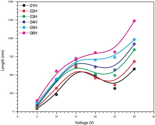
Figure 9 This figure lets to observe a strong dependence between length and the voltage used, which has a direct impact due to the growth speed (oxidation-dissolution). The reduction in the oxide growth velocity occurred in the range of 15 and 20 volts has a dependence with the dissolution rate. With this potential and this NH4F concentration, the dissolution is faster.
Figure 10 presents a comparison between the 36 samples, represented by points. The two main morphological parameters have been analyzed as a function of the Raman intensity of the vibrational mode E g (v6). The red points represent the length of the tube (nm), the blue points the diameter of the tube (units also in nm, divided by a factor of 10 for comparative purposes). These parameters have been introduced to show the strong relationship between them and E g (v6), which is also linked to the anodization time. It is a high dispersion in the data collected for the length, being more consistent for the diameter. The pink zone is related (by the recorded data) to the presence of nanopores and nanotubes of low diameter and length; the green zone limits the 3 parameters where a good matrix of nanotubes can be obtained; finally, the yellow zone is established for samples with a high presence of nanograss.
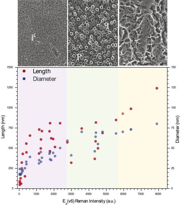
Figure 10 Comparison of 36 samples (dots) from a 6 x 6 matrix, where it has been synthesized and analyzed two variables (time and voltage) according to observe the behavior of the main morphological parameters. Red dots are used for tube length (nm), blue dots are used for tube diameter (nm). These parameters have been introduced in order to show the strong relationship between them and E g (v6) Raman Intensity linked also to anodization time.
It is presented in Fig. 11, using SEM images, the transition suffered by the titania nanostructure morphology (specifically the diameter) with anodization time from 1 to 6 hours (left to right) and a voltage from 5 V to 30 V (up to down).
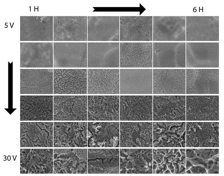
Figure 11 Scanning electron microscopy (SEM) micrographs of TiO2 nanotube layers by anodization in ethylene glycol, D.I. water, and NH4F, after the annealing process. Anodization time from 1 to 6 hours (left to right) and a voltage from 5 V to 30 V (up to down), these images let us appreciate the transitions and changes on the morphology of the titania nanostructures.
4. Conclusion
After the complete analysis of the whole set of samples obtained in this study, we can expose the final morphological results with the main intention to give a particular guide for next works related with TiO2 nanotubes in anatase phase and synthesized by anodization.
Increases the salt concentration will induce that the electrolyte increases their conductivity and the anodization speed (oxidation-dissolution) suffers also an increment. This important fact is to remark because that means we will have nanostructures in less time, and this is one of the main contributions of this study.
It has been possible to identify the conditions on which each structure has a strong presence due to its growth dynamics or its degradation. Each registered structure offers different surface area and different synthesis parameters, as follows:
Nanopores: range less than 10 minutes at a constant potential difference of 30 V, shown in group MI, but it is also possible to obtain it at low voltages in longer times.
Nanosponges: it happens due to the degradation (dissolution) of the pores, for a time lapse between 8 and 10 minutes for a constant potential of 30 V mainly.
Nanotubes: for a potential of 30 V in a time lapse from 10 to 40 minutes, for another potential, it exists in a range of 10 to 20 volts and a time lapse from 1 to 5 hours.
Nanoislands: as we mentioned above, it is produced by the collapse of the tubes occurring in a voltage range from 15 to 20 V and for a time lapse from 1 to 3 hours.
Nanograss: this structure has a partial or total presence for periods from 2 to 6 hours with a potential from 20 to 25 V mainly.
It has been observed, in the last pages, the strong relation between diameter - length - Raman intensity with the anodization voltage-time, but each parameter mentioned react in a different way (weaker or stronger dependence). Moreover, we offer in Table III, the complete data recollected for the ME group.
Table III Complete data of the main parameters of nanotubes, mentioned in this study.
| Sample | Voltage | Time | Diameter | Length | Raman Intensity | Sample | Voltage | Time | Diameter | Length | Raman Intensity | ||
|---|---|---|---|---|---|---|---|---|---|---|---|---|---|
| V | H | nm | nm | a.u. | V | H | nm | nm | a.u. | ||||
| ME | 1 | 5 | 1 | 17 | 45 | 45 | ME | 19 | 20 | 1 | 45 | 495 | 1250 |
| ME | 2 | 5 | 2 | 18 | 60 | 122 | ME | 20 | 20 | 2 | 45 | 461 | 1775 |
| ME | 3 | 5 | 3 | 18 | 71 | 44 | ME | 21 | 20 | 3 | 40 | 513 | 2066 |
| ME | 4 | 5 | 4 | 24 | 91 | 50 | ME | 22 | 20 | 4 | 44 | 612 | 1960 |
| ME | 5 | 5 | 5 | 17 | 125 | 90 | ME | 23 | 20 | 5 | 43 | 707 | 1750 |
| ME | 6 | 5 | 6 | 25 | 150 | 340 | ME | 24 | 20 | 6 | 50 | 807 | 2360 |
| ME | 7 | 10 | 1 | 20 | 234 | 170 | ME | 25 | 25 | 1 | 41 | 318 | 3000 |
| ME | 8 | 10 | 2 | 25 | 320 | 160 | ME | 26 | 25 | 2 | 46 | 366 | 4350 |
| ME | 9 | 10 | 3 | 22 | 428 | 215 | ME | 27 | 25 | 3 | 55 | 497 | 4530 |
| ME | 10 | 10 | 4 | 31 | 432 | 1150 | ME | 28 | 25 | 4 | 59 | 571 | 2775 |
| ME | 11 | 10 | 5 | 30 | 446 | 426 | ME | 29 | 25 | 5 | 70 | 742 | 3600 |
| ME | 12 | 10 | 6 | 33 | 555 | 420 | ME | 30 | 25 | 6 | 69 | 816 | 4415 |
| ME | 13 | 15 | 1 | 33 | 606 | 1260 | ME | 31 | 30 | 1 | 64 | 583 | 4396 |
| ME | 14 | 15 | 2 | 35 | 620 | 1850 | ME | 32 | 30 | 2 | 70 | 686 | 4792 |
| ME | 15 | 15 | 3 | 39 | 654 | 630 | ME | 33 | 30 | 3 | 68 | 847 | 5571 |
| ME | 16 | 15 | 4 | 38 | 710 | 1315 | ME | 34 | 30 | 4 | 70 | 925 | 5957 |
| ME | 17 | 15 | 5 | 35 | 729 | 1160 | ME | 35 | 30 | 5 | 73 | 986 | 6424 |
| ME | 18 | 15 | 6 | 36 | 807 | 1785 | ME | 36 | 30 | 6 | 80 | 1240 | 7911 |

