


 nova página do texto(beta)
 Inglês (pdf)
 Artigo em XML
 Referências do artigo
 Enviar este artigo por email
 Citado por SciELO
  Similares em
SciELO
Similares em
SciELO 
 Permalink
1. Introduction
Group III nitrides have been studied extensively because of their potential applications in optoelectronic devices, such as photodetectors [1], UV light emitting diodes (UV LEDs) and UV laser diodes (UV LDs) [2,3]. Aluminum nitride (AlN) has a direct band gap of 6.2 eV [4], a high thermal conductivity of 285 W m-1K-1 [5] and a high melting point (3273 K) [6]; characteristics useful in applications as GaN/AlN superlattice [7] and high-reflectance distributed Bragg-reflectors [8]. On the other hand, Al-AlN cermet thin films have been reported for several applications and recently as a solar absorber coating [9,10]. AlN films have been deposited with various methods, such as Chemical Vapor Deposition (CVD) [11], Metal-Organic Chemical Vapor Deposition (MOCVD) [12], Plasma-Source Molecular Beam Epitaxy (PSMBE) [13], reactive sputter deposition [14], molecular beam epitaxy [15] and Pulsed Laser Deposition (PLD) [16,17]. Particularly, PLD is a well suited method for depositing AlN thin films for optical applications since it is able to produce high-quality films at low deposition temperatures. An additional useful feature of PLD is its capability of deposition in a low-pressure reactive gas ambient [18].
The study of the formation of the compound AlN using a reactive atmosphere has been discussed in several works for instance Oikawa et al. reported the evolution of the Al bonding in AlN thin films grown by reactive deposition of thermally evaporated Al and RF excited nitrogen plasma [19]. Wang et al, reported the nitrogen bonding in aluminum oxynitrate films obtained by ion-beam sputtering [20]. The change in composition and chemical structure alteration by the bombardment of low-energy N2+ on single crystalline Al2O3 was studied by Espinós et al, [21]. Borges et al. showed the influence of the stoichiometry in the optical responses of AlNx Oy thin films deposited by reactive magnetron sputtering [22].
In this work we show the evolution of the chemical, structural and optical properties of thin films prepared reactively by ablating high-purity aluminum target in the presence of different pressures of nitrogen producing changes in composition up to the formation of the AlN film.
2. Experimental details
A set of five films with compositions from Al to AlN were grown reactively by changing nitrogen pressure using the pulsed laser deposition technique in a RIBER LDM-32 system equipped with in-situ X-ray photoelectron spectroscopy (XPS). A KrF excimer (λ = 248 nm) laser was utilized for the deposits. Laser energy, number of pulses and pulse repetition rate were fixed at 200 mJ, 27000 pulses and 5 Hz, respectively. The incident laser fluence was set at 4 J/cm2. The deposition was accomplished by ablating an aluminum target in a vacuum chamber with different pressures of high-purity molecular nitrogen. Nitrogen pressure was varied between 0 and 30 mTorr (0, 5, 10, 15, and 30 mTorr).The ablated material was collected on natively-oxidized Si(111) substrates at a temperature of 600°C. The base pressure in the growing chamber was kept within the 10-9 Torr range before each deposit. At the end of each deposition process, the samples were transferred in situ to the analysis chamber to carry out the XPS study. Morphology and cross-section characterization were made with a high resolution scanning microscope (HRSEM) Carl Zeiss Auriga. X-ray diffraction (XRD) was performed in a Philips X’pert MPD system using a Cu KαX-ray radiation source (λ = 0.15405 nm). XPS measurements were obtained using the Al Kα line of an X-ray source with energy of 1486.6 eV. After a general survey, high-resolution spectra in the regions of Al2p, O1s and N1s peaks were obtained. Due to the absence of a reliable carbon peak, the binding energy of the O1s line at 531.7 eV was taken as the reference peak to calibrate the binding energy of the obtained spectra. The Al2p and N1s peaks were fitted by employing asymmetric Gaussian-Lorentzian functions. The background subtraction was performed by using the mathematical model derived by Shirley. Uv-Vis reflection spectra of the films were measured using an Ocean Optics spectrometer, model USB2000.
3. Results and discussion
Figure 1 shows representative XRD patterns of corresponding samples deposited at: (a) 0 mTorr, (b) 15 mTorr and (c) 30 mTorr of nitrogen pressure. The diffraction peaks are indexed using the powder diffraction files 040787, 251133 and 391425, for cubic Al, hexagonal AlN and tetragonal SiO2, respectively. The diffraction range shown does not include the peaks related to Si because they have very large intensity as compared to the peaks from the film. The SiO2 (222) plane in the XRD patterns, is related with the native oxide of the Si substrate, this was used for normalize the other peaks. The thin film deposited at 0 mTorr of nitrogen pressure present only peaks related with Al, as can be seen in Fig. 1(a). Samples grown at 15 mTorr and 30 mTorr display peaks related with hexagonal AlN. A decrease in the strength of diffraction peaks related to Al as a function of nitrogen pressure. Diffraction peaks associated to AlN presented the opposed behavior indicating the successful formation of AlN as nitrogen content increases.
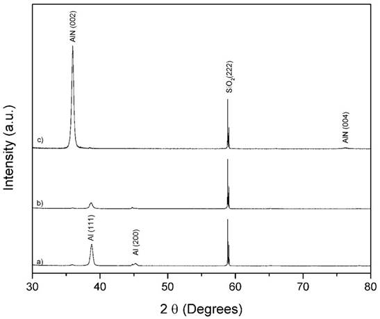
Figure 1 XRD patterns of samples deposited at a nitrogen pressure of: (a) 0 mTorr, (b) 15 mTorr, (c) 30 mTorr
Representative surface and cross section SEM images are shown in Fig. 2. Images correspond to the sample grown at 30 mTorr of nitrogen pressure. As can be observed in the cross section image presented in Fig. 2(b) a columnar growth processes is observed; the apparent double layer could be due a optical effect of the cross section. The thickness of this film was roughly 600 nm; similar thicknesses were observed for the other samples.
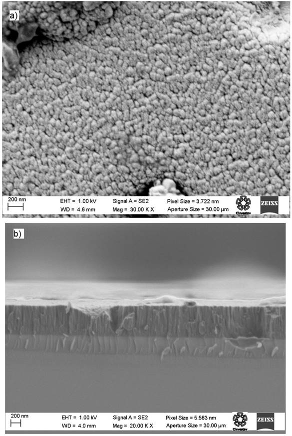
Figure 2 SEM images of aluminum nitride thin film deposited at a nitrogen pressure of 30 mTorr: (a) surface and (b) cross sectional.
Figure 3 shows a typical XPS survey spectrum of a film produced after ablating the Al target in a molecular nitrogen environment under a pressure of PN = 30 mTorr. Peaks related to aluminum, nitrogen and oxygen are clearly detected and no other elements are noticed. Intense photoelectrons 1s and Auger KLL peaks were observed for both N and O, in addition to the Al2s and Al2P peaks. As shown in Fig. 3 there is no carbon peak; therefore, the peak calibration was carried out using as reference the O1s peak characteristic of Al2O3 located at 531.7 eV [22]. It is justified because the binding energy of oxygen, in reactively obtained AlN thin films, has been reported to have the same value independently of the nitrogen incorporation in the film [20,23]. In order to corroborate our approximation, the samples were exposed to air, and then high-resolution XPS measurements were performed again. This time, XPS results presented the adventitious C1s peak due to surface contamination. This C1s peak maximum was utilized for charge referencing and the value obtained for the O1s peak maximum binding energy was 531.7 eV for all samples.

Figure 3 XPS spectrum of aluminum nitride thin film deposited at a nitrogen pressure of 30 mTorr and 600°C substrate temperature.
Because the binding energy of Al2p core level depends on the chemical state of the Al cation, the fitting of the Al2p XPS signal can be used to detect the different binding states of aluminum. The XPS data analysis was performed within the XPSPeak 4.1 program [23]. The Al2p XPS signal was fitted using mixed Lorentzian-Gaussian curves. Peak positions were fixed using the values reported in the XPS database of the National Institute of Standards and Technology (NIST) [24]. The adjustable parameter for fitting the spectra was the intensity of the peaks; while the Full Width at Half Maximum (FWHM) was fixed for all peaks.
Figure 4 shows the evolution of the high-resolution spectra of Al 2p signal for the five studied samples, from the sample deposited without nitrogen pressure up to a nitrogen pressure of 30 mTorr. The fitting of the Al 2p peak takes in account contributions from Al-Al, Al-N and Al-O bonds at binding energies of 72.3 eV (Al-Al), 73.1 eV (Al-N) and 74.5 eV (Al-O), [22]. When the thin film is deposited only in vacuum (without nitrogen pressure), the Al 2p peak has contributions from Al-Al and Al-O bonds (Fig. 4 (a)). For a nitrogen pressure of 5 mTorr during film growth, the same Al 2p peak presents three contributions, Al-Al, Al-N and Al-O bonds (Fig. 4 (b)). As the nitrogen pressure increases, a decreasing the signals associated to Al-Al bonds is observed. Small contributions of Al-O bonds are present in all cases. As it does not change with the nitrogen content, may be its origin comes from residual oxygen in the growth chamber.
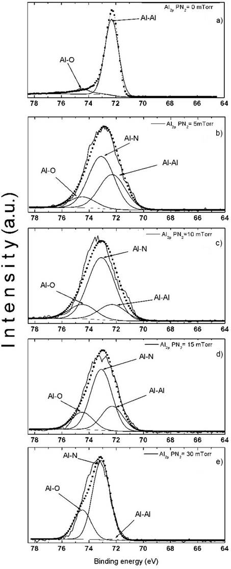
Figure 4 Evolution of Al2p peak, as measured by XPS, as a function of nitrogen pressure (a) 0 mTorr, (b) 5 mTorr, (c) 10 mTorr, (d) 15 mTorr and (e) 30 mTorr.
The assignment of peaks of N1s photoelectrons have been reported for AlN and Aluminum Oxynitride (AOL) films [19,20,25,26], these peaks were related with different oxidation states or chemical environment. High-resolution XPS spectra of N1s are displayed in Fig. 5. Spectra were decomposed into three peaks corresponding to N-O (397 eV), N-Al (396.2 eV) and N* (395.7 eV) bonds. The binding energies of N-O and N-Al were taken from reference [24]. The third peak, N*, can be related to a nitrogen bonded with pure aluminum. L. Rosenberguer et al. reported a peak at 395±0.3 eV for AlN films deposited by plasma source molecular beam epitaxy [26], they proposed that this peak is related to a nitrogen atoms with a coordination number of less than four. In Figs. 5(a), 5 (b) and 5 (c) the presence of a peak labeled as N* is observed. Then we propose that the N* peak is related with a nitrogen bounded with aluminum metal as for these samples there is a considerable aluminum content, as observed in Fig. 5. This observation is corroborated by the fitting presented in Fig. 5(d), this was carried out considering contributions of the peaks associated to N-O and N-Al. When we used a nitrogen pressure of 30 mTorr, we only had AlN and small amount of Al2O3, then could be expected that the peak N* (related wit Al metal) disappear.
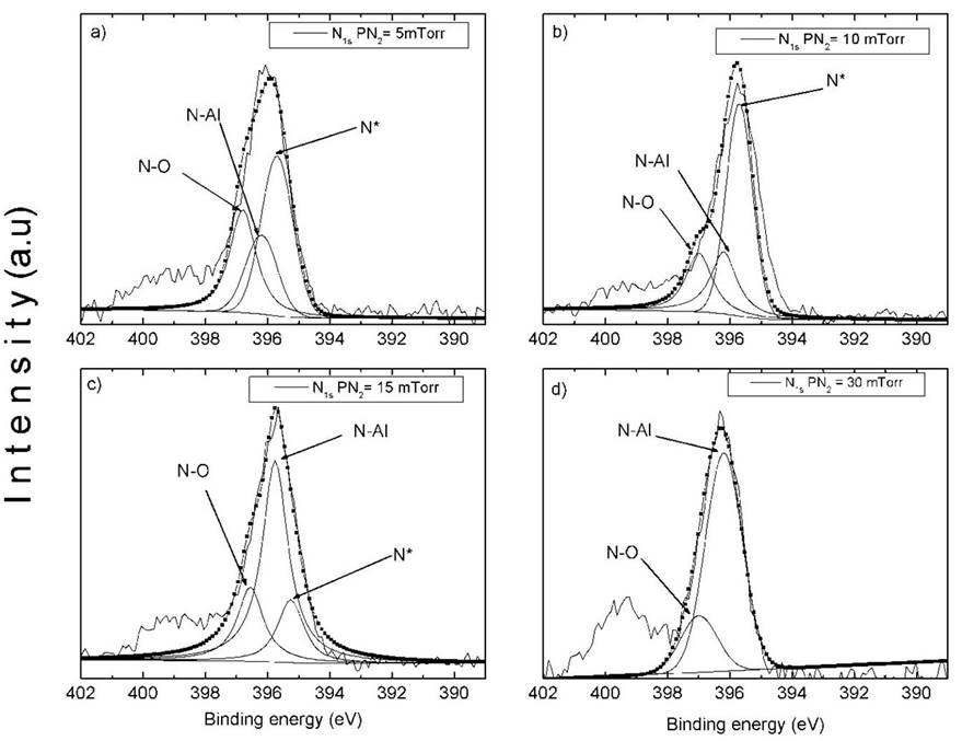
Figure 5 N1s peak deconvolution as a function of nitrogen pressure for the studied set of thin films, from Al to AlN.
An increasing on the nitrogen pressure will reduce Al metal percent with respect the Al corresponding to AlN and Al2O3; the saturation nitrogen pressure was 30 mTorr as we shown in the Fig. 4. Figure 6 shows the obtained reflectance spectra, only spectra with noticeable differences are included. The spectrum for sample prepared at 0 mTorr nitrogen pressure shows high reflectance, indicative of metallic behavior. When the nitrogen pressure is increased from 0 mTorr to 15 mTorr, reflectance decreases notoriously. For the sample produced at 30 mTorr an interference pattern typical for dielectric films that are transparent in the wavelength range is obtained. The results obtained were similar to the reported by Zhao et al. [27], for the optical properties of Al-AlN composite. In order to simulate the reflectance spectra of the samples, a commercial software SCOUT [28] was used. The dielectric function model, for opaque Al and AlN, were taken from reference [27]. The optical model, implemented in SCOUT was three layer material surrounded by air, constituted by air-deposited film-SiO2(8 nm)-Si-air. To fit the reflectance spectra, the model parameters plus the film thickness were used. The results (not presented here), shown good agreement between the experimental data and the optical model. The thickness obtained for the sample produced with 30 mTorr of nitrogen pressure, was 622 nm, in good agreement with the result obtained by SEM.

4. Conclusions
The controlled production of aluminum nitride thin films, with different proportion of metallic aluminum, was obtained by ablating an aluminum target in a N2 atmosphere at different pressures onto silicon wafer substrates at 600°C. The study of XPS high resolution spectra of the Al2p peak are evidences that the reaction between nitrogen and aluminum has occurred successfully. The film prepared using 30 mTorr nitrogen pressure has hexagonal phase of AlN and the interference features observed in its reflectance spectrum corroborates the successful production of the AlN film.

