


 text new page (beta)
 English (pdf)
 Article in xml format
 Article references
 Send this article by e-mail
 Cited by SciELO
  Similars in
SciELO
Similars in
SciELO 
 Permalink
1. Introduction
The increasing capacity of processing and storage of computers is reaching its limit with the current technology of transistors, based on the flow of electrons. In order to overcome these technological frontiers, it is necessary to go beyond charge states and consider the freedom degree of spin instead.
Nowadays, many studies, both theoretical and experimental, are carried out in order to control the spin of the electrons [1,2] and thus allowing to use it in the manufacture of a new type of very powerful computers. This task is not easy, however. It has been suggested the use of nanostructures, specially quantum dots (QD’s) for this purpose [3,4]. As shown in other works [5], an external magnetic field perpendicular to the direction of QD’s growth modifies the carrier spectra, however, there are few works mentioning how the wave functions are modified when the spin is included. It is important to see how the wave functions are modified because they determine matrix elements, for example. Regarding to the carrier energies, a factor that can also alters them is the addition, often accidental and uncontrollable during the QD’s growth, of impurities that lead to the modification of the expected confinement energies. With the aim of determining how much these impurities affect the carrier states we have analyzed the effect of a single impurity in the studied systems. This is important for some applications such as optical devices and solar cells [6-9].
In order to have a better understanding of the QD’s behavior, in this paper we
analyze the effect of the magnetic field, as a way to control the spin, and the role
of impurities on the carrier band structure of InAs/GaAs [10,11] and GaN/AlN [12,13] self assembled quantum dots (SAQD’s). Both systems
are studied in the framework of the eight-band
The impurity is considerated also as an additional potential and for simplicity, neglecting its volume and mass. It is assumed that intrinsic potentials such as deformation or piezoelectric ones are not affected by it. Specifically, we study the inclusion of an impurity in small QD’s, to see its effects on the carrier states of the nanostructures.
The paper is organized as following: In Sec. 2 a brief description of the
2.
It is well known that the multi-band
while for the wurtzite structure as in GaN/AlN QD’s, following Ref. [21], we use
where
where
where
An uniform magnetic field
Quantum dots, also known as artificial atoms due to their discrete energy levels, are
very susceptible to change their confining energies due to various aspects, such as:
the material that make them up, their size and shape, the distribution of the
intrinsic deformation potential in these systems, piezoelectric field and
dislocations [22]. Here it is
analyzed another way to modify their energy levels, besides the magnetic field, by
means of the presence of impurities. They play an important role as mentioned
before. The effect of an impurity has been included by means of a potential in the
diagonal of the Hamiltonian and the potential used for
where
3. Results
The Hamiltonian described in the previous section is solved by means of the finite element method [24]. We first present results corresponding to QD’s of InAs embedded in GaAs, under the action of a magnetic field, with a typical geometry of quadrangular pyramid whose base has 8 nm side and the height is 8 nm long [15,18]. Due to its crystalline structure (zinc blende), these materials do not have a considerable piezoelectric field, so in this calculation it was disregarded. Subsequently, similar results will be presented for GaN/AlN QD’s which have a geometry of truncated hexagonal pyramid [16,25] with dimensions from vertex to opposite vertex 18(8) nm in its lower(upper) part, a height of 4.1 nm and a wetting layer of 1 nm. Finally, the results obtained by including impurities in both systems are given.
3.1 InAs/GaAs QD’s under magnetic field
Figure 1 shows the effect of the magnetic
field on the distribution probability of the first four electron states in the
InAs/GaAs QD’s for
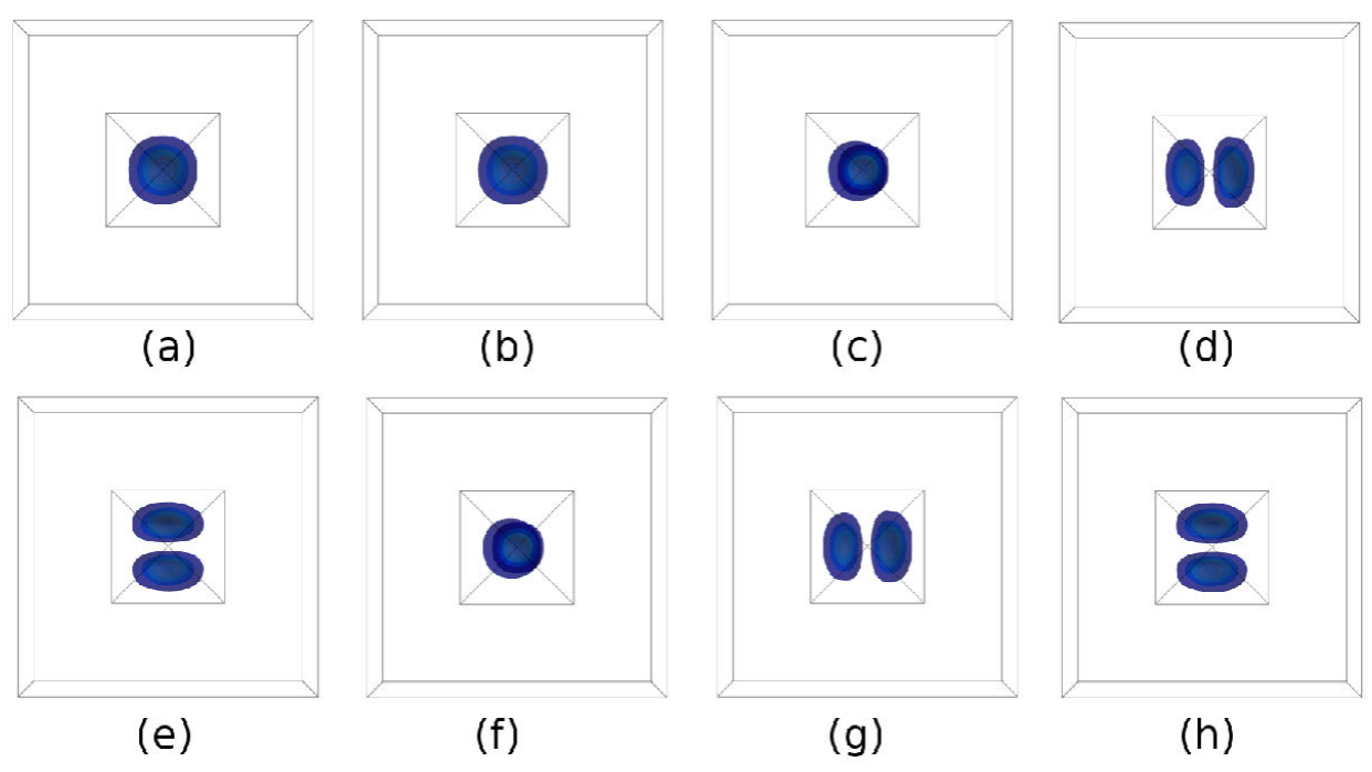
Figure 1 Top view of the electronic probability density for the first eight states: (a) e0, (b) e1, (c) e2, (d) e3, (e)e4, (f) e5, (g) e6 and (g) e7 state in InAs/GaAs QD’s with B = 20T.
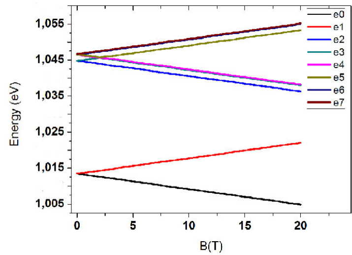
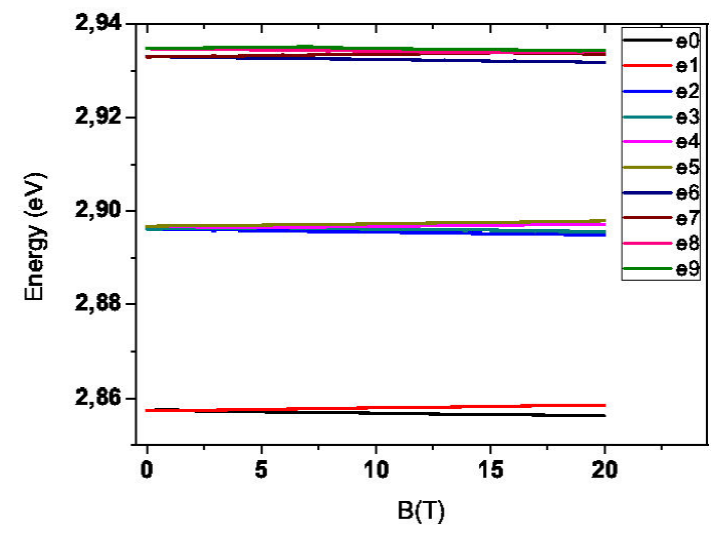
Figure 2 Carrier energy for the first 8 states of electrons in InAs/GaAs QD’s, varying the magnetic field B from 0T to 20T. Notice that the e3, e4 and e6, e7 almost overlap.
A quite different behavior is presented by the valence bands. In Fig. 3 the first four states corresponding to
the heavy-hole band are shown, under the effect of a magnetic field at different
intensities. Two main characteristics are observed: The states do not present a
typical distribution of
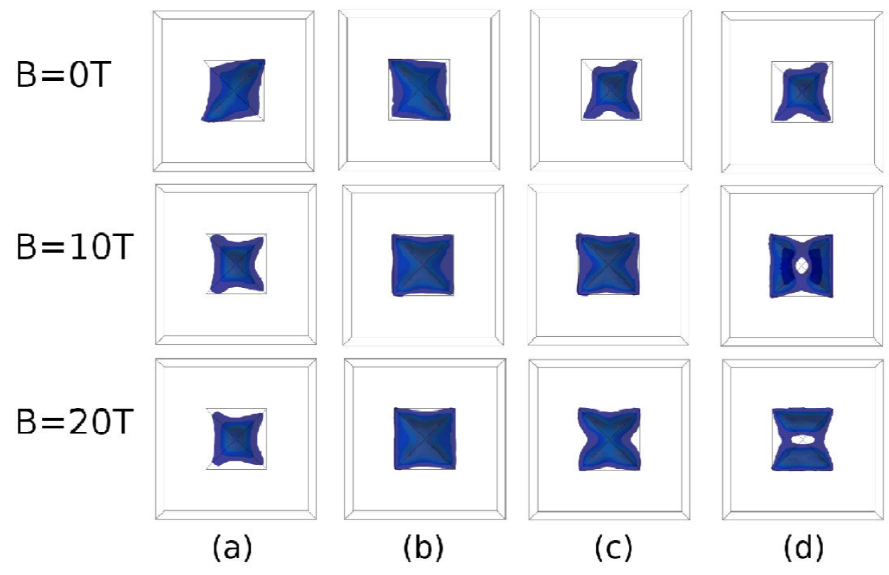
Figure 3 Top view of hole probability density of InAs/GaAs QDs for the first four states with values of magnetic field as show: (a) h0, (b) h1, (c) h2, and (d) h3.
The confinement levels in Fig. 4 also show
Zeeman behavior, i.e., the energy of the carriers with spin
down decreases, and the opposite occurs for the spin up as the intensity of
3.2 GaN/AlN QD under magnetic field
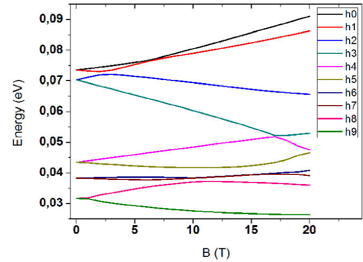
Now we analyze the effect of the magnetic field in a GaN/AlN QD. We begin with the analysis of the energy of the heavy holes. In Fig. 5 a very slight increase is observed as the magnetic field is increased, unlike the holes in InAs QD, this is due to the strong confinement that both carriers experience in the nitride system caused by the piezoelectric potential, which is as approximately 10 times bigger that the kinetic energy [16], depending of the position inside the QD and the carrier, (as seen in Fig. 8 below), which is small in InAs/GaAs QD. As in this latter system, an anti-crossing is present around 13 T between the states h7 and h8, it is important observe that the energy of all the states is similar.
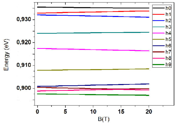
Figure 5 Carrier energy for the first 10 states of holes in GaN/AlN QD’s, as a function of the magnetic field B. Zeeman splitting is very small indicating strong confinement caused by the intrinsic piezoelectric potential.
The energy levels of the electrons have a very similar behavior shown by the
holes, as seen in Fig. 6. It is important
to note the bands are almost superimposed, showing a small effect of the
magnetic field compared to the strong intrinsic piezoelectric field. The states
e0-e1, e2-e5, e6-e7, and e8-e9 are degenerated in
3.3 Impurity in QD
As mentioned before, negative or positive impurities were included in both QD’s
systems, which correspond to a donor or an acceptor respectively. They were
placed at half the maximum height, with
Table I shows the carriers energies in the different QD’s systems considering the cases with and without impurities, the eigenvalues of Eq. (2). As it is observed, when the impurity is negative the carrier energy of the electrons for both systems decreases, with respect to the case without impurity. This is because the potential of the negative impurity repels the electrons, decreasing the effect of confinement, and in consequence its energy. On the other hand, the positive impurity attracts the electron, increasing the confinement effect and its respective energy. It happens the opposite to the holes, that is, the negative impurity decreases the carrier energy and the positive impurity increases it.
Table I Carrier energies for the different quantum dots with and without impuritites. Energy is given in eV.
| System | InAs/GaAs | GaN/AlN | |||
| carrier | electron | hole | electron | hole | |
| Type of Impurity | State | e0, e1, e2, e3 | h0, h1, h2, h3 | e0, e1, e2, e3 | h0, h1, h2, h3 |
| 1.0135 | 0.073539 | 2.8574 | 0.93286 | ||
| No impurity | 1.0449 | 0.073539 | 2.8961 | 0.93210 | |
| 1.0463 | 0.070252 | 2.8967 | 0.91746 | ||
| 1.0467 | 0.070248 | 2.9330 | 0.90042 | ||
| 0.9824 | 0.042249 | 2.7747 | 0.88951 | ||
| Negative | 1.0036 | 0.042246 | 2.8302 | 0.88854 | |
| 1.0042 | 0.024144 | 2.8307 | 0.87564 | ||
| 1.0281 | 0.024142 | 2.8721 | 0.85989 | ||
| 1.0549 | 0.13066 | 2.9321 | 0.97667 | ||
| Positive | 1.0800 | 0.13066 | 2.9575 | 0.97609 | |
| 1.0804 | 0.11111 | 2.9585 | 0.95977 | ||
| 1.1067 | 0.06831 | 2.9879 | 0.94119 | ||
Figure 7 shows a lateral view of the probability density of the ground state of electrons and heavy holes, without and with both types of impurities in a InAs/GaAs QD. It can be observed (Fig. 7a) that for the holes the charge distributions are slightly changed when the negative impurity is added, since they are strongly confined on the bottom of the QD and the impurity potential is not strong enough to deform the distribution. On the other hand, the repulsion of the positive impurity increases the energy of the holes and these are now confined into the region where the potential has a maximum energy, in this case, near of the top of the QD.
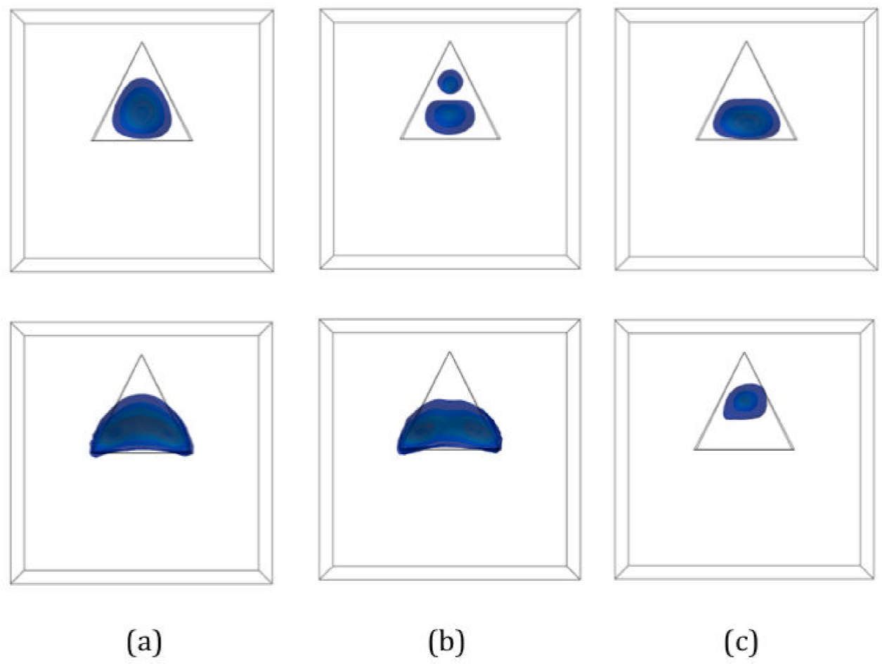
Figure 7 Lateral view of probability density isosurfaces for the first states for electrons (first row) and holes (second row) in InAs/GaAs QD’s: (a) without, with, (b) negative and (c) positive impurity. Calculated with B = 0.
On the contrary, electrons spread on the QD, such that a negative impurity splits
the distribution in two lobes (Fig. 7b)
while the positive impurity creates a spherical well potential with leads to a
complex competition between the confinement and the strain, causing the
wavefunction to be confined at the bottom of the QD. This redistribution of the
wavefunctions may affect the response of the QD. In the Table II several matrix elements involving the states e0, h0
and h1 are shown. These matrix elements play an important role in the analysis
of emission spectra, for example, since they are related to the rate transitions
in the dipole approximation. The matrix element represents the probability
transition of the electron in the conduction band to the valence band with the
emission of a photon through the coupling of an external electric field,
i.e., a larger matrix element indicates that is more likely
a emission, if the electric field is parallel to the corresponding direction
Table II Matrix elements for the state e0, h0 and h1 considering a negative, positive and without impurity
| InAs/GaAs | GaN/AlN | |||||
| Matrix element |
Without impurity |
Negative impurity |
Positive impurity |
Without impurity |
Negative impurity |
Positive impurity |
| <e0|x|h0> | 0.0101 | 0.1527 | 0.0185 | 2.2750×10⁻³ | 2.48-0×10−4 | 1.2141×10⁻² |
| <e0|y|h0> | 0.0028 | 8.88 × 10⁻⁴ | 9.55×10⁻⁴ | 1.5610×10⁻⁴ | 4.1569 × 10⁻⁴ | 5.4893×10⁻⁵ |
| <e0|z|h0> | 0.1480 | 0.1527 | 0.0381 | 1.7845 | 2.5315 | 1.7720 |
| <e0|x|h1> | 0.0021 | 0.0013 | 0.0062 | 4.0588×10⁻⁵ | 3.8031×10⁻⁶ | 4.0140×10⁻⁴ |
| <e0|y|h1> | 0.0049 | 0.0080 | 3.1630×10⁻⁴ | 1.4668×10⁻⁵ | 2.3963×10⁻⁶ | 5.0957×10⁻⁵ |
| <e0|z|h1> | 0.1445 | 0.1501 | 0.0111 | 3.687×10⁻² | 1.288×10⁻² | 7.9369×10⁻² |
In the case of the GaN/AlN system, the addition of impurities does not modify the probability density, this is again due to the fact that the piezoelectric field is very intense and creates confinement potentials in very specific areas, for the holes this zone is located below the QD within the wetting layer, and for the electrons it is located in the upper part of the QD (as reported in Ref. [16]). Figure 8 shows the probability density of electrons and holes calculated with zero magnetic field. Results are similar to those reported in previous works [1,5], where impurities are not included, confirming their almost null effect.
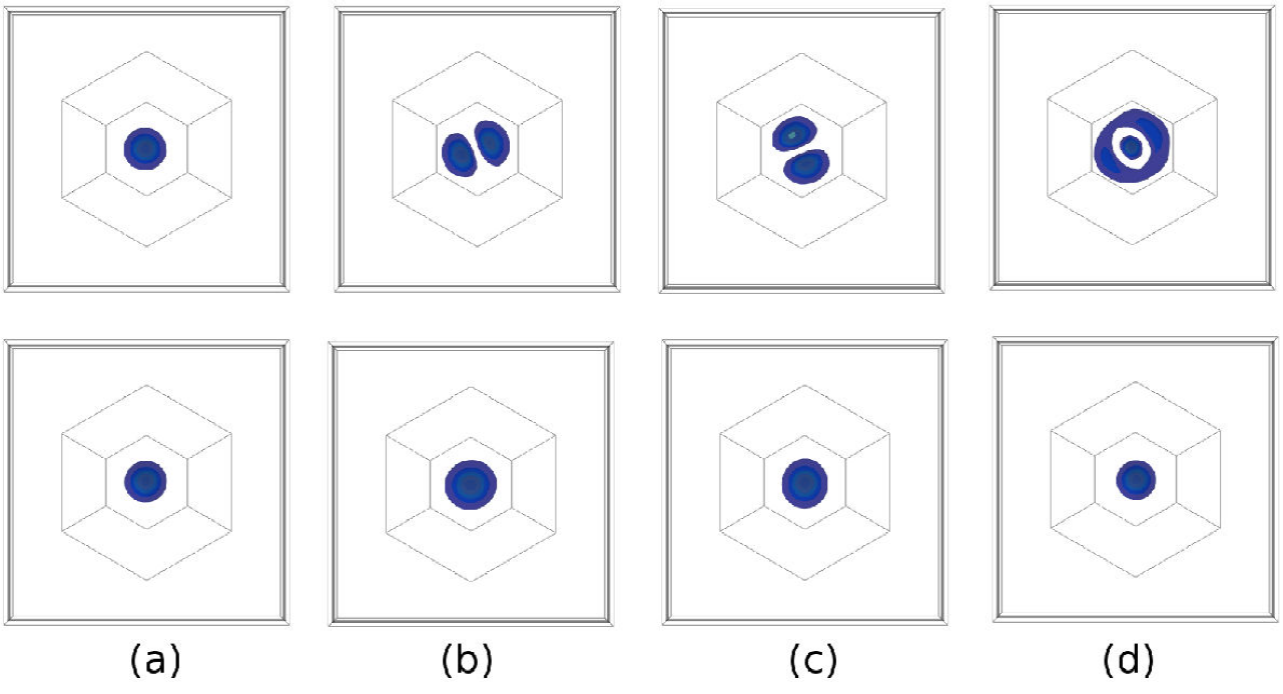
Figure 8 Top view of probability density for the first four states for electrons(up row) and holes(down row) in GaN/AlN QD’s: (a) e0/h0, (b) e1/h1, (c) e2/h2, and (d) e3/h3. Calculated with B = 0, considering a negative impurity.
Table II also shows the matrix elements
for the GaN/AlN QD’s. We can see that the probability is very small along the
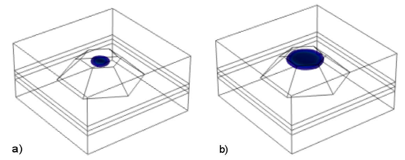
Finally we can see the effect of the position of a negative impurity on the electronic probability distribution inside the QD. In the Fig. 9(a) the impurity is at the center of the QD, with an energy of 2,4777eV, meanwhile in Fig. 9(b) is at the top of the QD, in this case the energy is 3.0062 ev. It is clear that the wavefunction in the latter case suffers a scattering due the repulsion between chargers.
4. Conclusions
The magnetic field provides a form to change the energy of the carriers. However, should be taken care at high values where anti-crossings appear, which may cause a disadvantage. We have observed the Zeeman splitting in both carriers as expected. However, the energy of the carriers in the system GaN/AlN presents only a small change, due to the strong piezoelectric confinement in this system, as compared with the InAs/GaAs QD’s, for which the effect is weak. Thus, energies of the InAs/GaAs QD’s change easily with the inclusion of the magnetic field, conversely the energy of the system of nitride QD it remains almost constant as the magnetic field increases.
Another form to change the carrier energy is through the inclusion of one impurity. Its effect depends on where it is located and on its type. As observed in the InAs/GaAs system, the probability density of both carriers without the impurity spreads almost around the entire interior of the QD. When a negative/positive impurity is inserted, its potential attracts/repels holes, or in opposite form, to the electrons. This causes a redistribution of the carriers, i.e., the effect of the impurities is similar to apply a low electric field [31-33].
The counterpart, the GaN/AlN QD system, presents a strong intrinsic confinement due to the piezoelectric field. The probability density is not affected by the inclusion of the impurity, since the effect of the impurity is small compared to the confinement. However, if the impurity is located close to the regions where electrons or holes are confined, it affects the distribution of one of the carriers only and the confinement energy is slightly changed, which makes the GaN/AlN QD’s less sensitive to the effects of the impurities, as long as these are not located in the zones of maximum confinement of the carriers. This is confirmed with the matrix elements, which change accordingly.
The magnetic field present a feasible way to modify the confinement energy and the probability density of the carriers in zinc-blende systems, which could be used in applications as quantum computing. The effect of the impurities is also important because it could explain some shifts in the photoluminescence spectrum in the quantum dots [25,34-36].

