Investigación
Physical properties of reactive RF sputtered a-IZON thin films
J.J. Ortegaa
C.R. Escobedo-Galvánb
F. Avelar-Muñoza
A. A. Ortiz-Hernándezc
H. Tototzintle-Huitlea
C. Falconyd
J.J. Araizaa
a Unidad Académica de Física, Universidad Autónoma de Zacatecas, Zacatecas, México.
b Centro de Estudios Científicos y Tecnológicos 18, Instituto Politécnico Nacional, Zacatecas, México.
c Departamento de Ingeniería en Mecatrónica, Universidad Politécnica de Zacatecas, Zacatecas, México.
d Departamento de Física, Centro de Investigación y Estudios Avanzados del Instituto Politécnico Nacional, Cd. México, México.
Abstract
The physical properties of amorphous indium zinc oxynitride (a-IZON) thin films, which were deposited at room temperature by reactive RF magnetron sputtering, were investigated. The results of the investigations indicated that the a-IZON films possessed excellent qualities: high transparency with a very low resistivity from 10-3
Ω⋅cm to 10-4 Ω⋅cm, while the carrier concentration showed values over 1020 cm -3 with mobility between 10 and 21 cm 2⋅V -1⋅s-1. The incorporated nitrogen reduces the typical crystallization of IZO and favors the deposition of transparent thin films. These results show that the IZON is an ideal amorphous material for applications in transparent and flexible optoelectronic devices.
Keywords: Indium zinc oxynitride; amorphous oxynitride; spectral ellipsometry; amorphous semiconductor; IZON
PACS: 71.15.Mb; 01.30.Vv
1. Introduction
Novel physical properties of oxynitride thin films have been the center of extensive investigations due to their properties and the potential applications in a wide range of electronic and optoelectronic devices. For example, monometallic and bimetallic oxynitrides have been investigated as catalysts 1, lithium phosphorus oxynitrides have been applied in thin film lithium ion batteries 2, titanium oxynitride has been developed for optical hard coatings 3, titanium niobium oxynitride has been applied in photocatalysis 4, indium and indium tin oxynitrides have been used for specific applications like gas sensors and high temperature thin film thermocouples 5, 6, aluminum oxynitride has been applied as transparent and conductive layers in optoelectronic devices 7, and zinc oxynitrides have been conceded as a strong substitute to conventional semiconductor film such as silicon due to high mobility value 8, 9. In this context, as general rule, amorphous oxynitrides have much higher charge carrier mobility than a-Si [10-12]. At the same time, amorphous oxynitrides presents homogeneous uniformity and high structural stability even though simple binary oxides tend to crystallize [13,14]. Moreover, the indium zinc oxynitride (IZON) is an excellent semiconductor for band gap engineering applications due to an easy tunable band gap [15,16]. Additionally, it was reported the use of a-IZON thin film on the channel layers of thin films transistors 17, and highlighted that the introduced nitrogen can help reduce oxygen vacancy in the channel layer, suppress carrier concentration and make the devices have a better threshold voltage.
Reactive sputtering is the predominant deposition technique employed to fabricate these oxynitride thin films and their properties are intimately dependent on the deposition parameters including deposition temperature, sputtering power and sputtering gas density, affecting directly to the structural and physical properties of IZON thin films. In a previous investigation 15, 18, it was found that by introducing nitrogen (N2) into the argon (Ar) plasma during the deposition of the indium zinc oxide by RF reactive sputtering, the properties of the deposited IZON thin films were very dependent on the amount of nitrogen in the plasma during deposition.
In the present study, the influence of sputtering power on the physical properties has been investigated in order to determine the optimum physical properties of IZON films. The deposition process and the optical, structural and electrical characterization of the IZON thin films obtained by RF reactive magnetron sputtering are presented. The nitrogen incorporation in the films is also studied as a function of the sputtering power used in the synthesis process. The refractive index and extinction coefficient were determined as a function of the photon energy using spectroscopic ellipsometry.
2.1. Thin film deposition and characterization.
Indium zinc oxynitride thin films were deposited on Si(100) substrates by reactive RF magnetron sputtering at room temperature and different sputtering powers. IZO (In2O3-ZnO, 90/10 wt.%, with a purity of 99.99%) was used as sputtering target. For this purpose, the deposition chamber was evacuated to a base pressure lower than 2×10⁻⁴Pa and the deposition processes were performed with Ar (99:995%) and N2 (99:99%) as the reactive sputtering gases at a total pressure of 0.8 Pa. These films were produced at a gas flow ratio of 10 sccm of N2 and 5 sccm of Ar, for different sputtering powers, which were changed from 60 to 120 watts as following: 60 W, 80 W, 100 W and 120 W. The deposited films were characterized in a Jeol Scanning Electron Microscope, model JSM-6390LV. This microscope was attached to an X-Ray energy dispersive spectrometer (INCA X-sight Oxford Inst. Model 7558). The crystalline structure of the IZON thin films was studied in a Siemens D-5000 diffractometer using the Cu Kα line (λ=0.1541 nm).The X-ray diffraction patterns were obtained in a grazing angle mode at 1.5∘. The electrical resistivity, mobility, and carrier concentration were measured in an Ecopia HMS-3000 Hall Effect Measurement System, using the Van der Pauw configuration. The optical transmittance was measured in a Perkin Elmer Lambda 35 UV-Vis spectrophotometer in the wavelength range from 300 nm to 1100 nm. Finally, SE measurements were acquired in a Yobin Ivon Ellipsometer, model UVISEL, in an energy range from 1.5 eV to 4.5 eV. The latter measurements were employed to find the refractive index (n) and extinction coefficient (k) of the films by comparison with the theoretical computer-calculated spectra of the films using the software provided with the ellipsometer, (Psi-Delta 2.0).
2.2. Spectral Ellipsometry Simulation.
A complete optical characterization of a semiconductor thin film can be made by the technique of spectral ellipsometry. SE is a nondestructive and noninvasive technique for the research on film structures and optical properties, including optical constants, grading profile and film thickness. It is particularly attractive because it is extremely sensitive to interfacial effects and surface roughness, for this reason, it can be applied to films having a thickness as small as monatomic to as large as several micrometers with high precision. The proposed IZON film structure used for SE analysis consisted of a substrate and three sublayers: interfacial layer of SiO2, IZON bulk layer and roughness layer. The IZON bulk layer was simulated using the classical dispersion model. For the roughness layer estimation, it was used a combination of the IZON bulk layer material and voids in different rates.
The expression for the classical dielectric function is presented in the Eq. (1), and it consists of four approaches which are the high energy dielectric constant, simple oscillator model, the Drude model and the double oscillator model as show in the following expression
ϵ=ϵ∞+(ϵs-ϵ∞)ωt2ωt2-ω2+iΓ0ω+ωp2-ω2+iΓDω+∑j=12fjω0j2ω0j2-ω2+iγjω
(1)
in this equation ϵ∞ is the high energy dielectric constant, ϵs is the static dielectric constant, ωt is the single oscillator resonance frequency, Γ0 is the single oscillator resonance width, ωp is the plasmon frequency and ΓD is Drude broadening parameter in angular frequency.
The knowledge of optical constants such as n and k is very important to determine the possible practical applications of a semiconductor film; the classical dispersion model is able to properly give the optical constants as well as some other parameters of quite importance.
3. Analysis and discussion of results.
3.1. Structural properties
3.1.1. Thickness
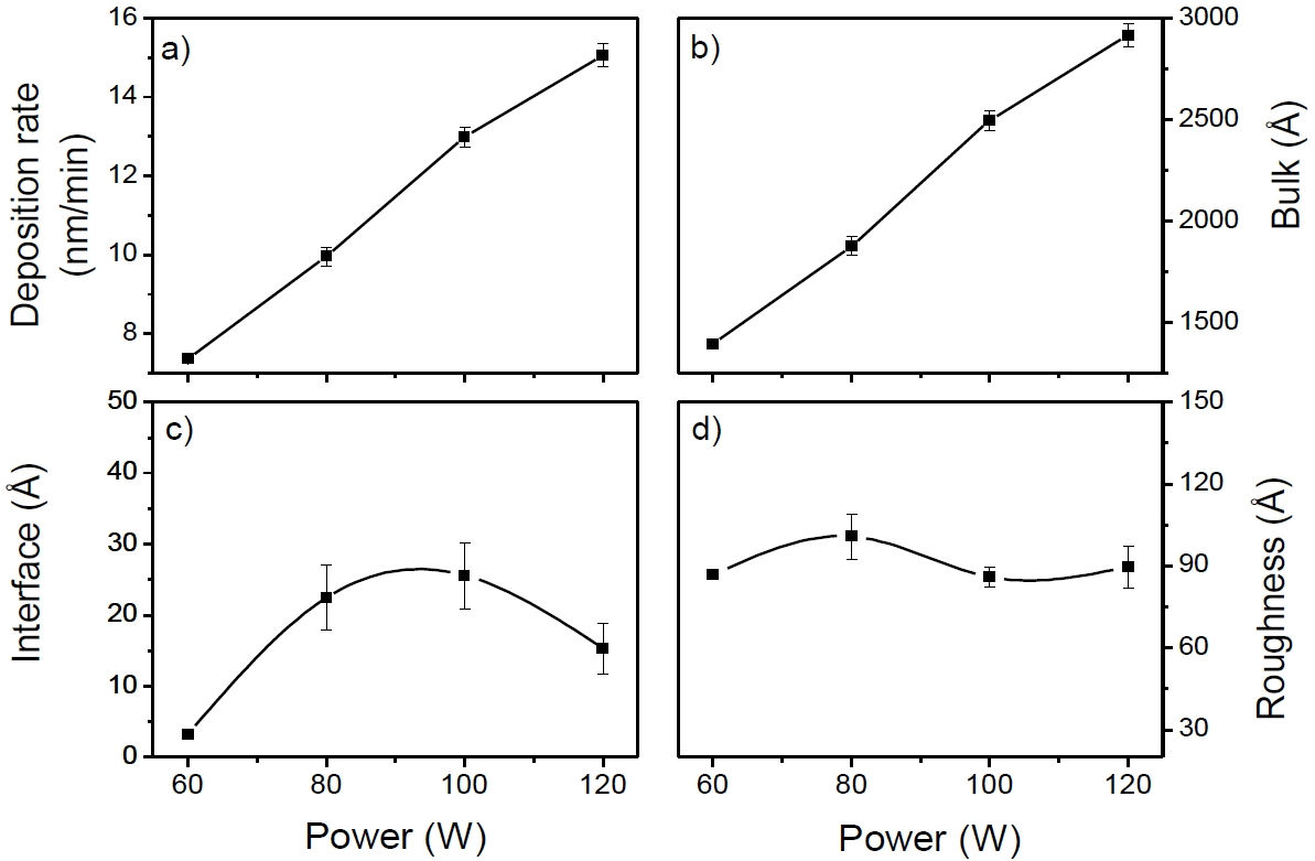
In Fig. 1, the deposition rate and the thickness of the sublayers components of the films structure are plotted. All these data were obtained directly from the parameters in the SE simulation. Figure 1 (a) show the deposition rate. It can be appreciated a linear increment of the deposition rate directly proportional to the increase of sputtering power. The same tendency is showed in Fig. 1 (b), where is presented the bulk layer thickness. When the sputtering power is increased, the ions in the plasma increase its acceleration, and as consequence, at the moment of the impact with the target, as the ionic species are more energetic, they transfer their momentum and energy to the exposed surface, this process led it to sputter more material from the metallic target and resulting in a higher deposition rate and a greater thickness films 15. The interface layer (Fig. 1 (c)) is a typically layer of native oxide (thickness lower than 30 Å) formed on the substrate due to the ambient exposition. Finally, the roughness is plotted in Fig. 1 (d), and it is not presenting any notable change as effect of the increment of sputtering power.
3.1.2. Atomic composition.
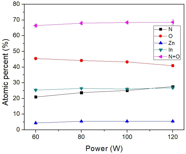
X-Ray energy dispersive spectroscopy (EDX) analysis confirmed the presence of In, Zn, O and N in all the deposited films. The atomic concentrations are shown in Fig. 2. As it was showed, the atomic percentages of indium and zinc in the films remained practically constant independently of the sputtering power used. However, as the sputtering power was increased, the amount of nitrogen in the films was increased too. At the same time, the percentage of oxygen in the film decreased, inversely proportional to the amount of nitrogen incorporated. This behavior can be explained from the growth kinetics of the sputtering process. When the deposit ion power is increased, the electric potential difference between the anode and the cathode increases too, which in turn causes an increase in the electric polarization of the N2 molecules, helping to excite them and putting the nitrogen in a reactive state which facilitates its incorporation into the film. In addition, the sum N2+O2 (also plotted) is nearly constant. These results directly suggest that oxygen ions are partially substituted by nitrogen ions in the film.
3.1.3. Crystalline structure
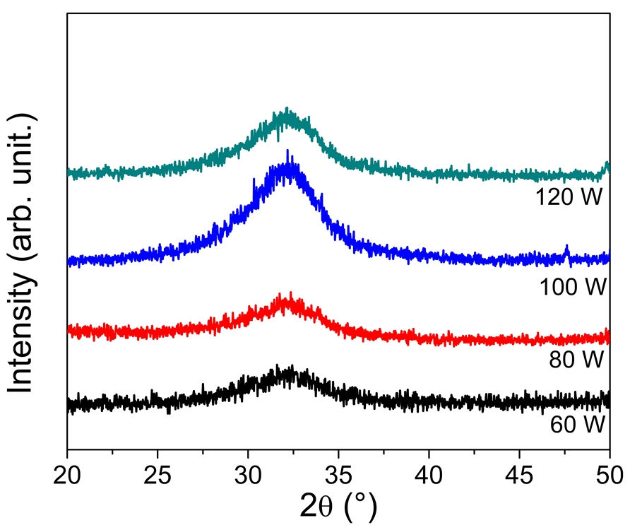
Figure 3 shows the XRD pattern obtained on the different films. All deposited films were amorphous, independently of the sputtering power used in the deposition, and the related spectra showed a broad band (bump) in the diffracted intensity associated with the amorphous phase in the range of 30∘-35∘ with the maximum approximately 32.4∘. This band is related to the amorphous IZO matrix, so it is not possible to observe evident effect of nitrogen for these cases however, it is well known that typically the IZO thin films tend to crystallize and the XRD pattern shows an intense, sharp peak at 2θ=33.2∘ related with the orientation (222) of pure In2O3
10-12, but in this case the IZON films showed a marked suppression of the typical crystallization of IZO, inclusive for the film deposited at 120 W.
3.2.Optical properties
From spectroscopic ellipsometry data and applying the Classical dispersion approximation, it was possible to determinate the complex refractive index ñ = n + ik, where the real part of the complex refractive index n is related to important physical properties of the semiconductor, and the complex part of the index of refractive coefficient k is directly related to the absorption coefficient (α), from which it is possible to obtain the forbidden band gap.
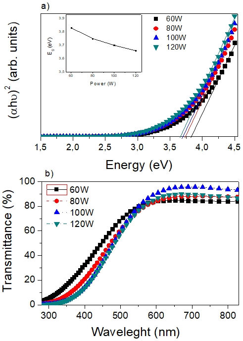
In Fig. 4, the values obtained for the complex refractive index are shown as a function of energy for the different sputtering powers. The real part of the complex refractive index (n) presents values above 2.0 for the initial energy of 1.5 eV and this value increases as the power of deposit increases. Additionally, the value presents a positive slope in the range of 1.5 to 3.2 eV; i.e., as the energy of the incident light grows the value of n increases to take a maximum value close to 2.4 for energy of approximately 3.2 eV. From this energy the slope is inverted and the value of the refractive index decreases. On the other hand, the extinction coefficient k shows a constant value, very close to zero, in the energy range between 1.5 eV and 2.0 eV and from this energy the extinction coefficient begins to increase almost linearly until a value of 0.515 for energy of 4.5 eV. This behavior is repeated for all films, regardless of the storage power; however, as power increases, the slope of the curve increases to reach higher values for the coefficient of extinction.
The extinction coefficient is related with the absorption coefficient by the equation α=4πk/λ, where α is the absorption, k denotes the extinction coefficient and λ is the wavelength associated to the photon energy. Using this equation is possible to determine the optical properties, which have been plotted in Fig. 5. The absorption spectra obtained from the SE data with the classical model are showed in Fig. 5(a). For all films, the optical absorption coefficient showed a similar behavior, however, for energies near to 3.8 eV the linear portion of the curves shifted systematically towards a lower energy, indicating a continuous decrease of the optical gap as an effect of the increment of nitrogen in the film. The optical band gap (Eg) was determined according to Tauc’s equation expressed as αhν=A(hν-Eg)l, where A is a constant, hν is the photon energy and the exponent is l=1/2 for allowed direct, l=2 for allowed indirect, l=3/2 for forbidden direct and l=3 for forbidden indirect transitions. Thus, the Eg can be determined by extrapolating the linear portion of the curves to zero absorption. In the case of IZON films, direct allowed transitions were selected (l=1/2), and this is related with previous reports of IZON and precursor oxides, such as ZnO 19, In2O3
20 and IZO 21.
The Tauc’s plots of IZON films (Fig. 5 (a)) showed that with the incorporation of N into the IZO host matrix clearly leads to a red shift on the optical response and a concomitant reduction of the band gap energy, as shown inset figure. These red shifts or band gap narrowing observed in absorption spectra can be attributed to the nitrogen incorporation; however, how N incorporated atoms change the band structure of the metal oxide host is still undetermined. Additionally, from the absorption spectra, if the multiple reflection of thin film is neglected, the optical transmittance is given by T=T0e(-αd), where α and d represent the optical absorption coefficient and the film thickness, respectively. Figure 5 (b) presents the optical transmittance in the wavelength range from 300 nm to 800 nm for IZON films deposited as a function of sputtering power. The transmittance for IZON thin films showed a red shift in the optical response for the Uv-Visible region. However, for wavelengths greater than 550 nm the transmittance values increased substantially reaching values greater than 90% of transparency, which can be explained by a decrease of oxygen vacancies in the film.
3.3. Electrical properties
Within the characterization of semiconductor materials, one of the most important is undoubtedly the analysis of the electrical properties. The density of charge carriers, mobility, type of electrical conductivity and resistivity are fundamental properties in terms of technological applications. There are direct and indirect techniques for measuring the carrier density, in direct techniques we can mention the Hall Effect measurement, which consists of the measurement of a voltage transverse to the direction of the current flowing through the thin film. This voltage is a result of the interaction of the current with a magnetic field perpendicular to it. On the other hand it is also possible to determine the electrical properties of a thin film by means of the interpretation of the parameters obtained from the model of Drude.
The carrier concentration (N) is related to the plasma frequency by the equation:
N=(ωp2m*ϵ∞ϵ0)e2
(2)
similarly, the mobility (μ) of the charge carriers is related to the Drude resonance width from the equation:
μ=eΓDm*
(3)
and finally, the resistivity (ρ) that is the inverse of the conductivity is expressed in terms of mobility and the concentration of carriers by means of the following relation:
ρ=1Neμ
(4)
3.3.1. Hall Effect Analysis
The carrier concentration, the mobility and the resistivity of the IZON thin films were analyzed as a function of the sputtering power. Figure 6 shows the dependence of the electrical properties as function of the sputtering power used for the deposition. In each picture are plotted the values directly measured by Hall Effect technique and the calculated values from the obtained SE parameters.
For the calculation of the electric properties, an effective mass of 0.3 times the mass of the electron was used, which is the average value reported for IZON films under similar conditions. All of the films presented n-type conductivity, which is the typical conductivity reported for IZON films. Moreover, all the IZON films presented a high carrier concentration with values over 1020 cm-3, independently of the used sputtering power; the highest value obtained correspond to the film deposited at 80 W and the film deposited at lower sputtering power (60 W) had the lowest carrier concentration, the values calculated from Drude parameters were consistent with the directly measured by Hall effect technique. Similarly, the lowest mobility with a value of 14 cm2⋅V-1⋅ s-1 was measured for the film deposited at 60 W, however, for the films grown at 80 W and 100 W the mobility increased until to reach a value maximum of 21 cm2⋅V-1⋅ s-1; finally, for the sample deposited at 120 W the mobility decreased until it reached a value of 19 cm2⋅V-1⋅s-1. Finally, it is seen that the resistivity of the IZON films decreases as a function of sputtering power and the best value was obtained for the IZON films deposited at 80 W with a value of 7.4×10⁻³Ω⋅cm. As a function of the deposition power the resistivity improves sufficiently for the film deposited at 80 W, reaching values almost equal to those reported for IZO films, however this tendency is not conserved and the resistivity of the films deposited at 100 and 120 W increased slightly due to the decrease shown in carrier concentration even when the mobility practically remains constant.
4. Conclusions
Amorphous IZON films were deposited on Si(100) substrates by radio frequency magnetron sputtering using the oxide ceramic In 2 O 3-ZnO target. The changes in structural, electrical and optical properties of the IZON films were investigated as function of the sputtering power used in the deposition. All the films presented a high transparency upon 500 nm in wavelength and the near infrared region; however, the nitrogen incorporation in the IZO matrix produces important changes in the physical properties of the IZO. The IZON films showed an amorphous structure and as effect of the incorporation of N into the IZO matrix, a red shift on the optical response was observed. The resistivity measured in the film presented values from 10-3 Ω⋅cm to 10-4Ω⋅cm, while the carrier concentration showed values over 1020 cm-3 with mobility between 10 and 21 cm2⋅V-1⋅ s-1.
Acknowledgements
This work was partially supported by Project UAZ-PTC-205. The authors are grateful to Zacarias Rivera, Angel Guillen and Marcela Guerrero for their technical assistance.
References
1. J. Park, and YC. Kang, Metals and Materials International, 19 (2013) 55-60. https://doi.org/10.1007/s12540-013-1010-9
[ Links ]
2. A. I. Saugar, C. Márquez-Alvarez, and J. Pérez-Pariente, Journal of Catalysis, 348 (2017) 177-188. https://doi.org/10.1016/j.jcat.2017.02.023.
[ Links ]
3. P. H. M. Bottger et al., Thin Solid Films 549 (2013) 232-238. https://doi.org/10.1016/j.tsf.2013.09.094.
[ Links ]
4. J. J. Brancho, A. D. Proctor, S. Panugantia, B. M. Bartlett, Dalton Transactions 46 (2017) 12081-12087. http://dx.doi.org/10.1039/C7DT03077K.
[ Links ]
5. X.H. Zhao, H.T. Li, S.W. Jiang, W.L. Zhang, H.C. Jiang, Thin Solid Films 629 (2017) 1-5. https://doi.org/10.1016/j.tsf.2017.03.044.
[ Links ]
6. M. Sparvoli, R. K. Onmori, F. O. Jorge, and M. A. Gazziro, IEEE Sensors Journal, 17 (2017) 2372-2376. https://doi.org/10.1109/JSEN.2017.2670080.
[ Links ]
7. X. Du, S. Yao, X. Jin, H. Chen, W. Li, and B. Liang, Journal of Physics D: Applied Physics 48 (2015) 345104. http://stacks.iop.org/0022-3727/48/i=34/a=345104.
[ Links ]
8. H. J. Kim, S. Y. Hong, D. H. Kim, H. S. Jeong, and H. I. Kwona, Journal of Vacuum Science & Technology B, Nanotechnology and Microelectronics: Materials, Processing, Measurement, and Phenomena 35 (2017) 030602. https://doi.org/10.1116/1.4983528.
[ Links ]
9. E. Lee, Scientific Reports 6 (2016) 23940. https://doi.org/10.1038/srep23940.
[ Links ]
10. T. Yamazaki et al., Applied Physics Letter 109 (2016) 262101. https://doi.org/10.1063/1.4973203.
[ Links ]
11. K. M. Niang, B. C. Bayer, J. C. Meyer, and A. J. Flewitt, Applied Physics Letter 111 (2017) 122109. https://doi.org/10.1063/1.5004514.
[ Links ]
12. J. T. Jang et al., ACS Applied Materials & Interfaces 7 (2015) 15570-15577. https://doi.org/10.1021/acsami.5b04152.
[ Links ]
13. H. Najafi, A. Karimi, D. Alexander, P. Dessarzin, and M. Morstein, Thin Solid Films 549 (2013) 224-231. https://doi.org/10.1016/j.tsf.2013.06.062.
[ Links ]
14. M. A. Carrillo Solano et al., Ionics 22 (2016) 471-481. https://doi.org/10.1007/s11581-015-1573-1.
[ Links ]
15. J.J. Ortega, M.A. Aguilar-Frutis, G. Alarcón, C. Falcony, V.H. Méndez-García, and J.J. Araiza, Materials Science and Engineering: B 187 (2014) 83-88. https://doi.org/10.1016/j.mseb.2014.05.005.
[ Links ]
16. N. Itagaki, K. Matsushima, D. Yamashita, H. Seo, K. Koga, and M. Shiratani, Materials Research Express 1 (2014) 036405. http://stacks.iop.org/2053-1591/1/i=3/a=036405.
[ Links ]
17. W. Nai-Qian, Z. Qun, S. Han-Ping, Journal of Inorganic Materials 31 (2016) 745-749.http://www.jim.org.cn/EN/abstract/article_13411.shtml
[ Links ]
18. J.J. Ortega et al., Journal of Materials Science and Engineering A,4 (2014) 91-98. https://doi: 10.17265/2161-6213/2014.03.004.
[ Links ]
19. U. Ozgur, Ya. I. Alivov, C. Liu, A. Teke, M. A. Reshchikov, Journal of Applied Physics 98 (2005) 041301. https://doi.org/10.1063/1.1992666.
[ Links ]
20. S. Kasiviswanathan and G. Rangarajan, Journal of Applied Physics 75 (1998) 2572. https://doi.org/10.1063/1.356231.
[ Links ]
21. N. Ito, Y. Sato, P.K. Song, A. Kaijio, K. Inoue, Y. Shigesato, Thin Solid Films 496 (2006) 99-103. https://doi.org/10.1016/j.tsf.2005.08.257.
[ Links ]


 text new page (beta)
 English (pdf)
 Article in xml format
 Article references
 Send this article by e-mail
 Cited by SciELO
  Similars in
SciELO
Similars in
SciELO 
 Permalink