


 nueva página del texto (beta)
 Inglés (pdf)
 Artículo en XML
 Referencias del artículo
 Enviar artículo por email
 Citado por SciELO
  Similares en
SciELO
Similares en
SciELO 
 Permalink
1. Introduction
Titanium dioxide material has been studied and used in areas like dye sensitized solar cells [1], hydrogen generation by water photo electrolysis [2], photocatalytic reduction of CO2 under outdoor sunlight [3], super capacitors [4], batteries [5], biomedical related applications including biosensors, molecular filtration, drug delivery, and tissue engineering [6, 8], because of the particular properties of TiO2 such as nontoxic, environmentally friendly, optical and electronic properties [9].
The high volume-area ratio, as a very important property of nanoscale [10], attracted significant attention from researchers, as it developed a new family of nanostructures, named for what they look like, e.g. nanorods, nanopores, nanowires, nanobelts and so on [11]. These structures can be obtained by physical and chemical synthesis methods [12, 14]. There is one special type of nanostructure, which has in fact a double area by default (inner and outer), that offers one direct and efficient pathway for electron transport [15] and a double surface, available for nanoparticles insertion [16], they are called nanotubes [17].
TiO2 nanotubes can be synthesized using anodic oxidation process (also called anodization), first reported in 2001 [14]. Anodization is an electrolytic process that creates a protective or decorative oxide layer. This versatile technique uses titanium (working as anode), usually foils, to obtain a vertically oriented nanotube matrix; the cathode is commonly a plate, rod or foil of pure platinum [18, 19] even when this material is too expensive. The process starts when a potential is applied [20], the anodization usually takes hours [21]. The anodized samples are cleaned in an ultrasonic bath frequently [22], or another mechanical method is to remove the residual structures such as nanograss, sponge or just a very thin oxide layer [23], because prolonged time or high concentration of salts can cause them to appear [24], for general purposes they need to be removed, even when the nanotubes suffer some alteration in their shape or top layer surface. As-anodized oxide layer formed, it is amorphous in nature [25], generally, crystallization is achieved through thermal treatment at 350-500oC [26] in a variety of atmospheres for high performance applications with anatase phase [27-29]. For specific applications, electrolyte selection is very important [30], commonly used NH4F salts and ethylene glycol due the biocompatibility in the biomedical field [30].
The main goal in this study was to identify the time lapse in minutes, where a TiO2 nanotubular matrix can be obtained with no presence of nanograss and exclude the ultrasonic bath or another mechanical method, in order to remove it. A good tube shape, a vertical alignment and a free top layer, are necessary characteristics for a better performance in almost all applications; moreover, an important factor in this study was the selection and use of graphite as an effective alternative cathode, due to low cost and optimal nanotube morphology.
2. Experimental
Titanium foils (15×15×0.1 mm) were firstly used as an anodic electrode, while pure graphite rods (35×6 mm) were used as cathodic electrode. Titanium foils were cut in smaller foils (15×5×0.1 mm), then they were cleaned by ultrasonication successively in ethanol, deionized water and acetone. The distance between electrodes was constant in every experiment (30 mm). The foils were anodized from 10 to 60 minutes in organic electrolyte: ethylene glycol, 2% deionized water and 1.2 wt% NH4F; using two electrode configurations.
The anodization was carried out using a DC power source under constant voltage of 30 V, the schematic diagram of the anodization set-up is shown in Fig. 1.
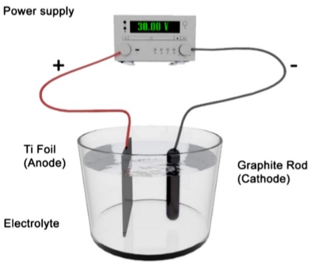
FIGURE 1 3D Schematic diagram of the anodization set-up (two electrode configuration). Organic electrolyte consists of ethylene glycol, 2% deionized water and 1.2 wt% NH4F.
After anodization process, the whole set of anodized samples was rinsed in deionized water, dried and then annealed at 400oC for 4 hours in air. The morphology and structure of TiO2 nanostructure was characterized by Field Emission Scanning Electron Microscope (SEM) (JSM-7600F, JEOL), Raman spectra were obtained on a DXR Raman Microscope (Thermo Scientific) using a 532 nm laser, 50X objective, 10 mW power, 50 µm slit and 3 s time collection.
3. Results and discussion
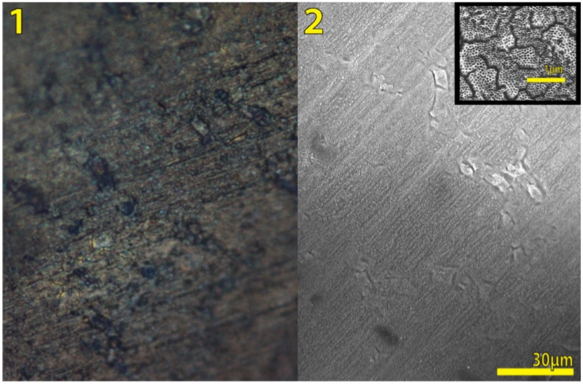
At a first glance, Fig. 2 remarks how TiO2 nanotubes suffer a degeneration over a top layer surface. For more details, Fig. 2 shows in 1), 2) and 3) a good nanotube layer with a very little presence of residual thin oxide layer, it is formed in the first stage of growth [31] for a time of 10, 20 and 30 minutes respectively, even this oxide layer can be easily removed when rinsed in D.I. water thoroughly, or Nitrogen beam, here the nanotube diameter is around 52-53 nanometers, which is a good size for insertion of nanoparticles for example, so it is very important to remark this time lapse where it is possible to have a good shape of tubes; 4) This micrograph demonstrates how the nanotubes start to collapse, forming clusters of bundled nanotubes (also called islands), this is due to the surface stress originating during formation of the oxide films [32] and an irregular topology of substrate; 5) here it is very clear to see how the nanotubes are collapsed due to be grown by extended anodizing time, often a disintegration of the top end of nanotubes due to chemical dissolution is observed, and then the nanotubes transform into TiO2 nanograss [33, 34]; 6) It clearly shows a full presence of well-formed nanograss, where the nanotube diameter is around 62-65 nanometers due to time progress under the same voltage, this diameter size is still suitable for general purpose.
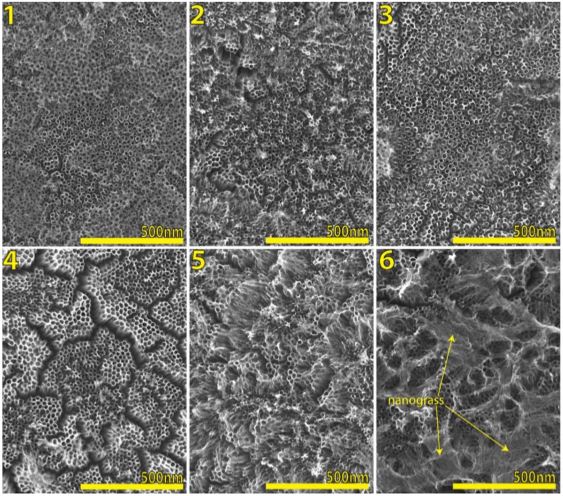
FIGURE 2 Scanning electron microscopy (SEM) micrographs of TiO2 nanotube layers by anodization under constant voltage (30 V) in ethylene glycol, D.I. water and NH4F, after annealing process. Anodization time of: 1) 10 min, 2) 20 min, 3) 30 min, 4) 40 min, 5) 50 min, 6) 60 min, here is indicated the nanograss presence.
The change from an amorphous state (as-anodized sample) to crystalline phase, as result after the annealing process to 400oC during 4 hours in air, can be confirm through Raman spectroscopy. As per literature report, there are six Raman active modes of anatase phase: A1g (515 cm−1), 2B1g (400 and 519 cm−1), 3Eg (144, 197 and 640 cm−1) [35]. Figure 4 clearly shows the peaks obtained experimentally.
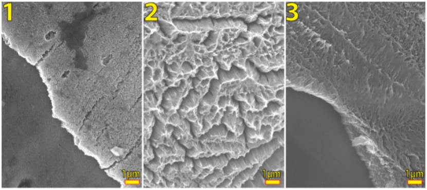
FIGURE 3 Perspective SEM micrographs of anodized samples by 1) 10 min, where there is just nanotube presence, 2) 30 min, where is clearly to see how the nanotubes are collapsed; 3) 60 min, there are a strong presence of nanograss.
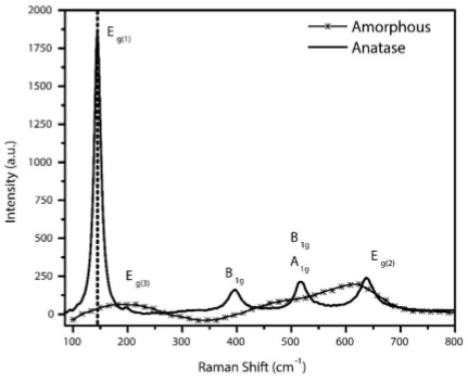
FIGURE 4 Raman Spectra of one anodized sample, dash line show as-anodized sample and after annealing treatment to 400oC with solid line. There are clearly visible as the six Raman active vibrational modes for anatase phase A 1g , 2B 1g , 3E g .
Figure 5 shows a close up from 130 to 156 cm−1 (1) with the whole set of Raman spectra (six anodized samples), it is possible to see and observe how the Raman intensity suffers an increment due to oxide thickness, it is progressive as a time function. There is a little change in Eg. (1) peak position, from a theoretical Raman shift 144 cm−1 (indicated by vertical red dashed line) for TiO2 nanotubes films [36] and if this result is compared to SEM micrographs it is possible to observe how this vibrational mode appears with the bigger displacement of 1.1985 cm−1 for a anodization time of 10 minutes, and as we know based in Fig. 2, for this anodization time, there is just a vertically oriented nanotubes layer, very thin after all with a tube length of 335 nm; 20, 30, and 50 minutes exhibit a decrement about the shift; 40 and 60 minutes have an increment (blue shift) and we can associate it with the presence of nanotube islands and nanograss (Fig. 2). Alhomoudi et al. explained this relation between Eg shift, Raman intensity and oxide thickness, trough experimental and analytical study, it has been demonstrated that when thickness increases, the decreasing of Eg shift exists, until standard position (144 cm−1) and this Eg Shift is due to stress between substrate and oxide layer [37] also it has been recognized that residual compressive stresses may cause film delamination from the substrate whereas tensile stress may cause surface cracks in the film, similar to nanotube islands and micro surface cracks (Fig. 6). The dominant 144 cm−1 Eg mode is shifted towards a higher frequency by an amount that depends on the substrate as well as on the thickness of the film. The compressive stresses gradually increase with lower film thickness, which means that the stress gets higher closer to the film and substrate interface. The shifts of the 400 cm−1 B1g and 640 cm−1 E1g modes were toward lower wave numbers and decrease with film thickness. Similar behavior has been related to the confinement effects in nanostructured anatase crystallites [38-41].
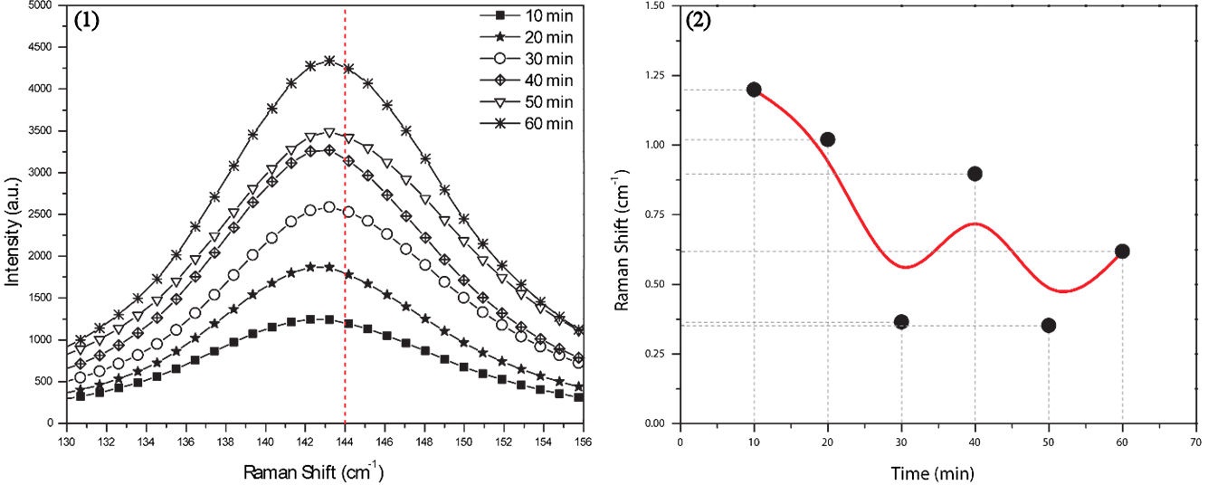
FIGURE 5 The whole set of anodized samples was analysed by Raman Spectroscopy. It is possible to identify a change in Eg(1) vibrational mode: Intensity due of the thickness (1) and Raman shift due to stress (2).
4. Conclusion
Amorphous TiO2 nanotube layers, produced by titanium anodic oxidation, can be studied and used for general purpose, but for high performance, and take advantage of more special features, this oxide layer can be crystallized into pure anatase phase, through the annealing process under 350-500oC. As a main target to have nanotubes without presence of nanograss and with no use of cleaning mechanical procedures, a time lapse under specifically conditions (pH, electrolyte concentration, voltage and temperature) can be obtained from 10 to 30 minutes, even 40 minutes and still be a clean nanotube sample. Due to the time of anodizing and constant voltage, these nanotubes are sub-micrometric in size and these can be used to Surface Enhanced-Raman Spectroscopy applications without problem.

