


 text new page (beta)
 English (pdf)
 Article in xml format
 Article references
 Send this article by e-mail
 Cited by SciELO
  Similars in
SciELO
Similars in
SciELO 
 Permalink
1. Introduction
The semiconductor quantum dot active region takes full advantage of the quantum confinement effect. The three dimensional quantum confinement of carriers results in discrete carrier energy level structure in a quantum dot active region [1,3]. Consequently, the quantum dot laser diode offers the potential performance in high optical gain [1,2], low threshold current density [2,4] and high characteristic temperature [1].
The use of quantum dots in nitride semiconductors is more effective, since the zero-dimensional electronic states in the QDs play an essential role for improving optical gain and threshold current characteristics particularly in wide bandgap semiconductors.
III-nitride based devices are of particular interest due to their wide range of emission frequencies and their potential for high-power electronic applications [5]. The band gap energy ranges from 0.7 eV for InN, 3.4 eV for GaN to 6.2 eV for AlN [6]. By adding Indium and Aluminum to GaN, ternary alloys can be formed with wide bandgap range of from 0.7 to 6.2 eV, which can cover the spectral range from deep ultra violet (UV) to infrared (IR) at room temperature [7,8].
In this work, we analyze the optical gain and threshold performances of the GaN/Al 0.2 Ga 0.8 N quantum dots lasers, based on the density matrix theory of semiconductor lasers with relaxation broadening [2] including the effect of doping and side length of quantum box.
The optical gain and threshold current density represent the basic elements that must be optimized to produce a high performance quantum box laser, and are also important elements in the study and comparison of the effect of p-type doping and n-type doping in GaN/Al0.2 Ga0.8 N.
2. Theoretical background
2.1. Optical Gain Theory
Taking into account the intraband relaxation in the same way as in Ref. [2], the optical gain of quantum box lasers active region is given by:
Here the subscript c (or v) denotes the conduction band (or heavy- hole band), where f c and f v are the corresponding Fermi functions for electrons in the conduction and valence bands given by:
Where ε cn et ε vn are the total energies of electrons and holes for subbands n.
E cv is a transition energy between the conduction band and valence band, R cv is the dipole moment, ω is the angular frequency of light, ε 0 and µ 0 are the dielectric constant and permeability of the vacuum, τ in the intraband relaxation time (τ in = 0.1 ps), n r is the refractive index and g cv is the density of states for the QD, given by [2]:
Where δ(E) is the delta function, and E cnml and E vnml are the quantized electron and hole energy levels respectively of a quantum box structure in x, y and z directions, respectively [9]. If we assume a structure consisting of GaN/Al 0.2 Ga 0.8 N quantum box with a dimension of L x , L y and L z , energy levels are expressed by the following equation, where the barrier height in the potential profile is assumed to be infinite [10]:
Where
In Eq. (1), we have supposed that the electron and hole in the quantum box are in equilibrium determined by the quasiFermi levels E fc and E fv respectively.
E fc and E fv are related to the electron and hole densities injected into the quantum box as [2,7]:
In the approach of Eqs. (1), (5a) and (5b), we have assumed the transition from the first conduction band to the first valence band (heavy hole band) because the density of states of light hole band is smaller than that of the heavy hole band and it’s probability to occur is more significant than of the other transitions .
2.2. Effects of impurities doping
The presence of donors or acceptors can be accounted by replacing N in Eq. (5a) by N + N d and N in Eq. (5b) by N + N α .
Where N d and N α are the donor and acceptor densities respectively [10,11].
2.3. Threshold current density
The threshold carrier density is calculated using the following equation [12]:
Where α i is internal loss, α is differential gain, Γ is optical confinement factor, L c is cavity length and N tr is transparency carrier density.
The threshold current density using threshold carrier density (N th ) is written as [2,14,15]:
Where q is electron charge, η is the rate of surface area of quantum boxes included in the whole area, n is the number of the layers of quantum box array and τ s is carrier life time.
3. Results and discussion
It’s assumed that the quantum dot structure studied has a GaN in the form of cubic active layer of L side length (L = L x = L y = L z ) sandwiched between Al 0.2 Ga 0.8 N barriers (Fig. 1), using quantum box model we calculate quantum dot quantized energy levels for conduction and valence bands which are implemented in the model described above to calculate the optical gain . The parameters used in calculation are listed in Table I.
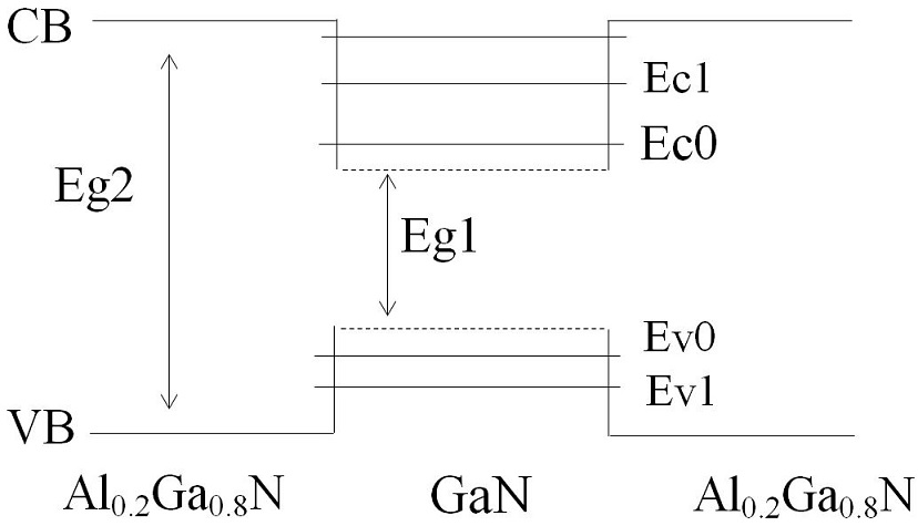
FIGURE 1 One-dimensional scheme of the band diagram of GaN based quantum dot. CB: conduction band; VB: valence band; Eg1: band gap of GaN; Eg2: band gap of Al0.2 Ga0.8 N, Ec0/Ev0 are ground quantized energy levels of electron and hole in CB and BV respectively.
TABLE I The parameters used in the calculations (m 0 is the free electron mass)
| GaN | AlN | |
| Band gap energy(E g (eV)) | 3.43 | 6.2 |
| Electron effective mass(m e ) | 0.2 m0 | 0.3 m0 |
| Heavy hole effective mass(m hh ) | 0.8 m0 | 1.14 m0 |
| refractive index n r | 2.67 | 2.03 |
| Spin orbit splitting ∆ cr (eV) | 0.019 | -0.164 |
Figure 2 presents a comparison between optical gain spectra of undoped structure for GaN quantum dot and pdoped structure with acceptor densities N a = 5×1018 cm−3 and n-doped structure with donor densities Nd = 5 × 1018 cm−3 at side length of quantum dot L = 60 Å and injection carrier Nv = 2 × 1019 cm−3, where we observed a higher optical gain value in p-doped structure than that in undoped or n-doped structure.
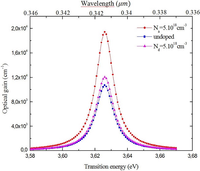
FIGURE 2 Optical gain versus transition energy of undoped structure compared with gain spectra of p-doping (N α = 5 × 1018 cm−3) and n-doping (N d = 5 × 1018 cm−3) for GaN/Al0.2 Ga0.8 N quantum dot laser at L=60 Å, N v =2×1019 cm−3.
The p-type doping effectively decreases f v since N is increased to N + N α , causing an increase in f c − f v . On the other hand, n-type doping does not give rise to significant increase in f c − f v when N is increased to N + N d .
In Fig. 3, the optical gain is plotted as function of the photon energy for various side length of a cubic quantum box for p-doped, undoped and n-doped structures respectively; it is observed that the gain is higher at L = 60 A for both cases˚ due to the increase of carrier density for population inversion in small size quantum box. On the other hand, when the size of the quantum dot increases, the carriers in the box are distributed over useless levels, and the separation between energy levels is not enough to obtain high gain. It should also be noted that the p-doped structure has the best value of maximum gain compared to the other structures.
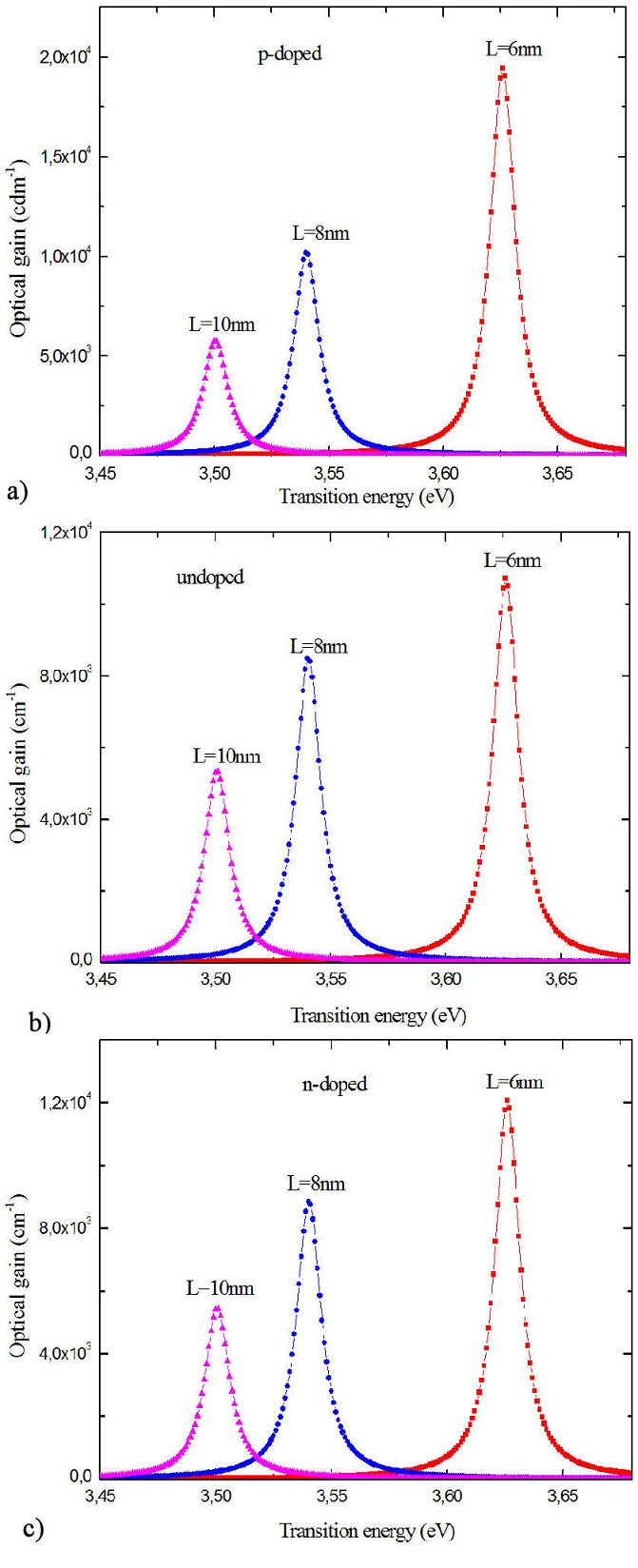
FIGURE 3 Gain spectra of p-doped (N α = 5×1018 cm−3), unpoded and n-doped (N d =5×1018 cm−3) for GaN quantum dot laser for different sizes of quantum box at N v =2×1019 cm−3.
Figure 4 shows the high sensitivity of maximum gain to changes in carrier density for different values of quantum box’s size of p-doped, undoped and N-doped structures respectively.
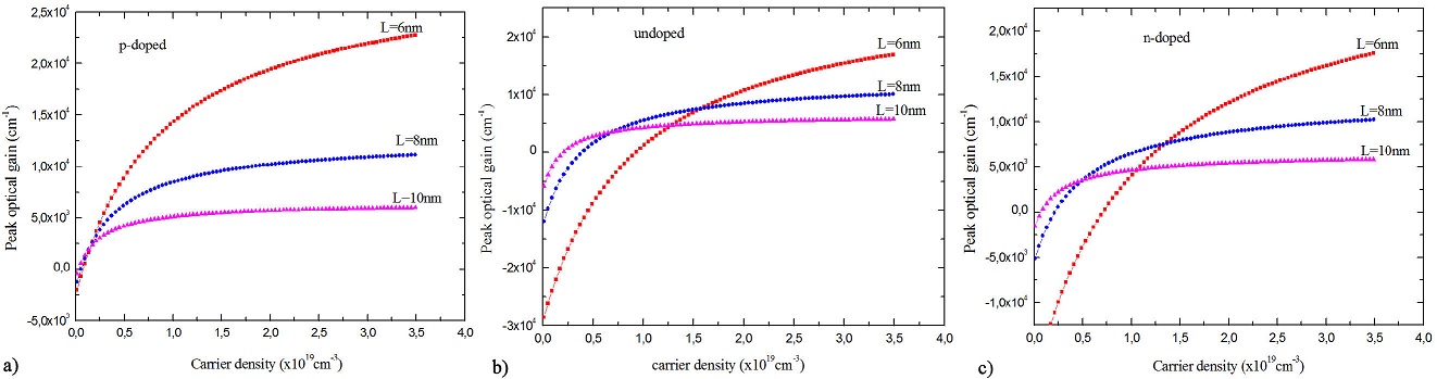
FIGURE 4 Dependence of peak optical gain on carrier density in GaN QD of p-doped (N α = 5×1018 cm−3), unpoded and n-doped (N d =5×1018 cm−3) structures for different sizes of quantum box at N v =2×1019 cm−3.
It shows also for both cases, two regions (positive side) and absorption (negative side) and that give us the value of the transparency density N tr from which the material begins to amplify the photon whose energy satisfies the conduction of Bernard-Duraffourg (E g < hν < E fc −E fv ) for each box size (where hν is photon energy).
The modal gain is also a fundamental characteristic for lasing action in hetero-structures. It is obtained by multiplying optical gain with confinement factor. When the modal gain overcomes the total loss, the lasing action takes place. It is expressed as: g m = Γ · g where Γ is optical confinement factor.
The variation of modal gain on current density values for different sizes of quantum box of three structures p-doped, undoped and n-doped is plotted in Fig. 5. This last figure is particularly useful because it shows the interrelation among the three parameters of interest: gain modal, current and side of length of QD, and allows immediate comparison between different quantum dots.
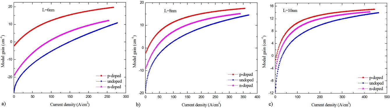
FIGURE 5 Modal gain as function of current density for GaN/Al 0.2 Ga 0.8 N QD structure for different sizes of quantum box of p-doped (N a =5×1018 cm−3), unpoded and n-doped (N d =5×1018 cm−3) structures at N v =2×1019 cm−3.
From this figure: we observe a parabolic increase for initial values of the current density but it saturates afterwards indicating very small or negligible increase in modal gain with change in current density, we note also, that the transparency current density Jtr (intercept at gain =0), which is the value at which the active layer neither absorbs nor amplifies the light at the lasing wavelength, decreases with increasing of the side length of quantum box. Moreover, the slope of the gain versus current density plot decreases with increasing of the side length of quantum box.
For laser oscillation, the modal gain must equal the total losses ®total. The laser oscillation condition is given as [16,17,18]:
Assuming that αi = 5 cm-1, R = 0:3, n = 1 and Lc = 4:2 mm, the threshold current density Jth that corresponds to the modal gain value that satisfies the oscillation condition can be obtained from the modal gain-current density plots [19,20].
From these curves and Table II summarizing the results, we can deduce that the p-type doping makes it possible to increase the gain peak and to reach an emission threshold for low carrier concentrations relative to the undoped or n-doped case, which makes it possible to achieve at minimum values of threshold current densities, and that the optimum size of the cube for lowest threshold is shifted to longer length of the side because low gain can be achieved without carrier injection for the useless levels. Which gives that the optimal structure is p-doped structure with L = 100 Å, the value of the gain is 5897 cm-1 and the minimum value of threshold current density is about 52.38 A/cm2.
TABLE II Performance characteristics of GaN/Al 0.2Ga 0.8N QD structure for different sizes of cubic quantum box of p-doped (N a = 5×1018 cm−3), unpoded and n-doped (N d =5×1018 cm−3) structures at N v =2×1019 cm−3.
| p-doped | undoped | n-doped | |||||||
| Side length (Å) | 60 | 80 | 100 | 60 | 80 | 100 | 60 | 80 | 100 |
| Gain max (cm−1) | 19545 | 10483 | 5897 | 10909 | 8608 | 5420 | 12500 | 8948 | 5478 |
| Transition energy (eV) | 3.626 | 3.54 | 3.5012 | 3.626 | 3.54 | 3.5012 | 3.626 | 3.54 | 3.5012 |
| Peak wavelenght(nm) | 342 | 350 | 354 | 342 | 350 | 354 | 342 | 350 | 354 |
| Emission spectrum | UV | UV | UV | UV | UV | UV | UV | UV | UV |
| Ntr (×1019 cm−3) | 0.073 | 0.06 | 0.019 | 0.926 | 0.391 | 0.2 | 0.71 | 0.215 | 0.075 |
| Transparency current J tr (A/cm2) | 9.35 | 8.83 | 6.72 | 148.37 | 69.67 | 33.4 | 91.1 | 37.57 | 15.58 |
| Threshold current density J th (A/cm2) | 56.68 | 56.2 | 52.38 | 237 | 178.1 | 136 | 176 | 108 | 78.3 |
4. Conclusion
In this paper, we have investigated the optical gain characteristics of GaN/Al0.2Ga0.8N quantum dot laser and the effect of doping and size of quantum dot on its performance. We have presented also the modal gain characteristics of GaN/Al0.2Ga0.8N QD for both structures. The variation in modal gain with increasing current density has been plotted with the effect different sizes of quantum box. The following findings can be stated: the effect of p-doping is efficient by increasing gain; n-doping has less effect and gain increases with reducing quantum box size. The results indicate also that better performance can be achieved with GaN/Al0.2Ga0.8N p-doped quantum dot laser with L = 100 A° compared to undoped and n-doped structure.

