


 nueva página del texto (beta)
 Inglés (pdf)
 Artículo en XML
 Referencias del artículo
 Enviar artículo por email
 Citado por SciELO
  Similares en
SciELO
Similares en
SciELO 
 Permalink
1. Introduction
The most important role of solid-state electronic ceramic components known as varistors (nonlinear resistors) is to sense and limit transient voltage surges. For this reason, they have been extensively used to protect electronic equipment from overvoltage [1]. Varistors are characterized with respect to other devices by two essential aspects, namely: i) symmetry (the same value at different voltage polarities) and nonlinearity (the resistance decreases with the applied voltage) [2]. The current-voltage (j(E)) characteristic of a varistor is usually calculated using the equation j = kE α , where j is the current density, E is the electrical field, α is the nonlinear electrical coefficient, and k is a constant related to the material microstructure [3]. The greater the value of α, the better the device to protect an equipment.
Tin dioxide (SnO2) is an n-type semiconductor with a wide direct band gap of 3.6 eV at 300 K [4], with a rutiletype structure and space group
The effect of In2O3 content on the microstructure and electrical properties of SnO2-based varistors has been investigated previously by different authors, doping the ceramics with Co-Ta [15] and with Co-Nb [16]. Despite the difference in the second dopant (Ta or Nb), in both studies it was concluded that variations of electrical properties are attributed mainly to variations of grain size. However, and more specifically, in addition to variations of grain size, in the case of Co-Ta doped samples, the variations in electrical properties are also attributed to resistivity of grain boundaries, whilst in the case for Co- Nb samples, the increase of breakdown electrical field with increase in In2O3 content is ascribed only to the decrease of grain size. Taking everything into account, it is apparent that the use of Ta is promising for attaining a higher non-linear coefficient (α).
Whilst the prior investigations have focused mainly on studying the effect of low and medium levels of additions of In2O3, to the best of the author’s knowledge, no previous work has reported results from the effect of high levels of addition of In2O3 to SnO2-based ceramics. Preliminary work by the authors suggests that high quantities of addition of In2O3 impact significantly the grain size in the microstructure of the ceramics. On that context, the aim of this work was to investigate the effect of In2O3 additions - emphasizing on high addition levels - on the microstructure, physical and electrical properties of SnO2-Co3O4-Ta2O5 ceramics.
2. Materials and methods
Analytical-grade SnO2 (Aldrich), Co3O4 (Aldrich), In2O3 (Aldrich) and Ta2O5 (Aldrich) powders were used as the starting materials for sample preparation. The molar composition of the investigated systems was (98.95-X) % SnO2-1 % Co3O4-0.05 % Ta2O5-X % In2O3, where X = 0.0, 0.05, 0.1, 1 and 2%. The powders were mixed through high-energy milling performed for 20 minutes in a planetary ball-mill (Pulverisette 7, Fritsch GmbH) using vials and balls of agate. The resulting powders were uniaxially pressed in the form of tablets (0.9 mm in diameter) at 230 MPa without the use of binders.
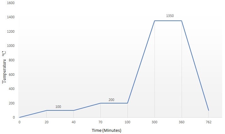
The tablets were sintered in a tube furnace (Nabertherm RHTH 120/300/1700). Maximum sintering temperature was 1350oC for 1 h. The sintering cycle is fully described in Fig. 1. Both ends of the tube furnace were capped with ceramic fiber. After cooling down to room temperature, the samples were removed from the furnace to be prepared for characterization. The density of the sintered samples was determined by Archimedes’ method and the linear shrinkage γ was calculated according to the expression:
where D 0 and D are diameters of the sample before and after sintering, respectively.
All ceramic systems of the present study were characterized by means of thermalanalysisintherangeof 30to 1500oC in a simultaneous TG-DSC-DTA equipment (TA-Instruments model SDT Q600). Samples of 20 to 30 mg were placed in the thermal analyzer within a platinum crucible and heated at the rate of 10oC/min in static air, using alumina as reference material. The temperature range was established in order to corroborate the occurrence of the spinel phase Co2SnO4 in the temperature range, as reported previously [17]. All samples were analyzed under the same thermal conditions.
The determination of phases was conducted by X-ray diffraction technique (XRD; PANalytical Empyrean model) with CuKα radiation (λ = 1.5406 Å) operated at 45 kV, 40 mA and a Pixel 1D detector in Bragg-Brentano geometry. The scans were performed in the 2θ range from 10 to 100o with a step scan of 0.016o and 20 s per step in a continuous mode. Phase identification was performed with X’Pert HighScore Plus software, version 4.6, and the ICDD PDF-4 plus database (ICDD International Center for Diffraction Data, Newtown Square, PA). The microstructure of the samples was characterized by scanning electron microscopy (SEM; model Nova Nano SEM 200, FEI). The mean grain size was determined from SEM micrographs with the aid of an image analysis software (Image-Pro Plus), according to the ASTM-E112 standard procedures.
For electrical characterization, equal silver electrodes were placed on both faces of the sintered ceramic specimens. Current-voltage measurements were conducted using a High Voltage Measure Unit (Keithley 2410). The nonlinear coefficient α was determined at a current density of 1-10 mAcm−2 using the following equation:
where E 1 and E 2 are the applied electric fields corresponding to the current densities J 1 = 1 mAcm−2 and J 2 = 10 mAcm−2, respectively. The breakdown voltage E B was measured at 1 mAcm−2. J and E can be calculated by means of i/s and V/t, where i is the electric current, s is the area of silver electrode and t is the thickness of the tested sample.
3. Results and discussion
Figure 2 shows representative SEM photomicrographs of all specimens taken at the same magnification for comparison purposes, from the specimen with 0 % In2O3 (Fig. 2a) to that with 2 mol % In2O3 (Fig. 2e).
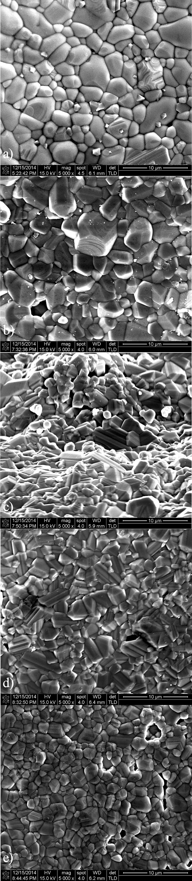
FIGURE 2 SEM micrographs of samples sintered at 1350o C for 1 hour: (a) 0.00, (b) 0.05, (c) 0.1, (d) 1 and (e) 2 % In2O3.
Although there is no manifest appearance of equiaxed grains - particularly for specimens with 0.1 and 1 mol % In2O3 (Figs, 2c and 2d, respectively) -, there is, however a tendency in grain size reduction, markedly observed in the specimen with the highest level of In2O3 (2 mol %, Fig. 2e). The mean grain size (l g ) of specimens prepared with all compositions is reported in Table I, showing that at the highest level of In2O3 (2 mol %), a grain reduction of about 43 % is reached, compared with the specimen without In2O3 addition. Despite the observed grain size reduction, shrinkage (γ) does not seem to be influenced by the addition of indium oxide, being also the case for the measured density. The magnitudes of density, relative density, grain size and shrinkage are all summarized in Table I.
TABLE I Shrinkage (γ), measured density (ρ), relative theoretical density (ρ tr ), mean grain size (l g ), nonlinearity coefficient (α) and electric field at fixed current density (E 1) of the samples doped with different contents of In2O3
| In2O3 (mol %) |
γ (%) |
ρ (g/cm3) |
αρtr (%) |
lg (µm) |
α |
E
B
(V/cm) |
| 0.00 | 10.87 | 6.61 | 95.43 | 2.1 | 10.72 | 1551.40 |
| 0.05 | 11.07 | 6.57 | 94.87 | 2.20 | 10.80 | 2053.44 |
| 0.1 | 11.18 | 6.60 | 95.30 | 1.89 | - | - |
| 1 | 10.58 | 6.47 | 93.34 | 1.44 | - | - |
| 2 | 11.03 | 6.31 | 91.00 | 1.24 | - | - |
α Theoretical density of SnO2 is 6.95 g/cm3.
Representative X-ray powder diffraction patterns of noncalcined and calcined samples are shown in Fig. 3. For non-calcined samples doped with 0.0, 0.05 and 0.1 mol% (Fig. 3a), the identified peaks correspond to Co3O4 with cubic structure (ICDD PDF # 04-003-0984) and SnO2 with tetragonal structure (ICDD PDF # 04-005-5929), while in the case of doped samples with 1 and 2 mol %, the presence of the above mentioned phases was observed, together with In2O3, with cubic structure (ICDD PDF # 04-008-2461) (marked as •, ∗, ◦, respectively), suggesting an excess of In2O3 in those samples. XRD patterns from samples 0.05 and 0.1 mol% show no evidence of In2O3 since the content of this oxide is below the limit of detection of the equipment. In the case of calcined samples (Fig. 3b), SnO2 (tetragonal) still prevails common to all compositions, but the reactants Co3O4 and In2O3 are not present anymore, at least within the detection limits of the equipment. Moreover, for calcined specimens with 1 and 2 mol%, the presence of SnO2 with cubic structure, is observed (ICDD PDF # 00-033-1374). Since the solubility of In2O3 in SnO2 has been reported [18] to be about 96.1-94.4 mol % SnO2 (3.9-5.6 mol % In2O3), and as no free In2O3 was identified by the diffractometer, the authors suggest that indium oxide was incorporated into the SnO2 lattice modifying its crystal structure from tetragonal to cubic. Although the spinel phase Co2SnO4 is not detected by conventional XRD analysis, analysis by DTA/TGA reveals an endothermic peak at 920oC, which in accord to previous works by the same research group, corresponds to spinel formation [17,19].
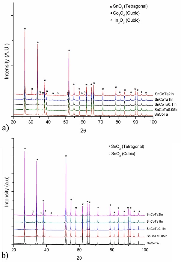
FIGURE 3 XRD patterns of SnO2 ceramics with different indium oxide contents: (a) for non-calcined samples and (b) calcined samples.
Figure 4a shows what appears to be a habitus of SnO2 single crystals formed during sintering on the surface of samples. The color of these crystals went from pale pink to purple as the In2O3 content increased. Crystals with hollow needlelike shape are observed at high magnification (Fig. 4b). The surface crystals formed during sintering were analyzed by XRD. A set of diffraction patterns are shown in Fig. 5. First, a crystal was carefully removed from the surface of the ceramic disc and placed in a zero background holder. The resulting pattern is labeled as Setting 1. Then, the sample holder with the sample on it was rotated by 90o with respect to the previous setting. The resulting pattern is presented as Setting 2. Finally, the crystal was powdered in an agate mortar. The corresponding XRD pattern is labeled as Powdered Crystal. Identified peaks correspond to tetragonal SnO2 (ICDD PDF # 4 01-072-1147); according to this card, and following the intensity order, the three most intense diffraction planes were identified and indexed. The difference in intensity is relate to preferential crystallographic orientation. Authors suggest the high content of In2O3 had a noticeable effect for the occurring of the formation of SnO2 habitus on the surface of samples since at lower contents this outcome had not been previously reported.
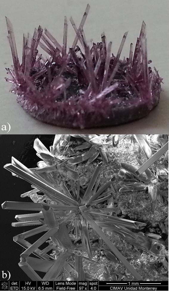
FIGURE 4 Photograph showing crystal formation on the surface of ceramic sample (a). SEM micrograph displays detailed hollow needle-like shape of crystals (b).
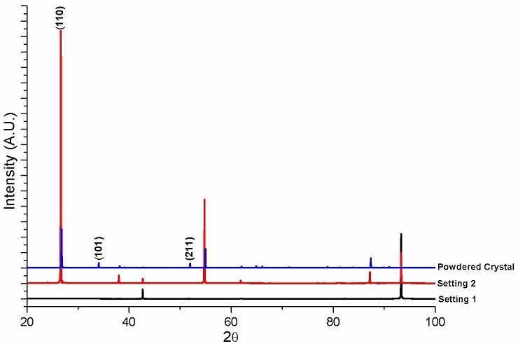
FIGURE 5 Diffraction patterns of a crystal taken from the surface of sample showing preferred orientation.
Results from the differential thermal analyses for all compositions before sintering are shown in Fig. 6. The thermograms indicate the presence of a main endothermic peak associated to the spinel (Co2SnO4) formation at the temperature of 920oC. At high temperatures, Co3O4 decomposes into CoO as reaction product, following the reaction equation:
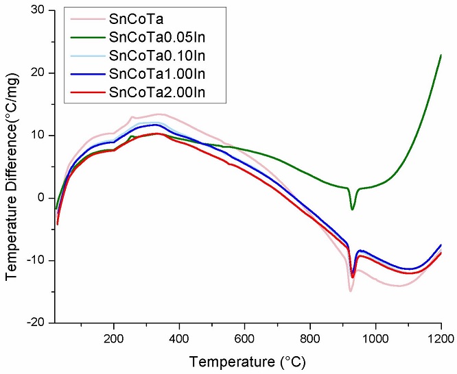
Once the CoO is obtained, and since SnO2 is present, then the formation of the spinel phase follows the reaction given by:
Details on the formation mechanism of the Co2SnO4 phase detected by DTA/TGA are reported elsewhere [17,19].
The reason why specimens with 1 and 2 % In2O3 does not reveal formation of the spinel phase In4Sn3O12 is found on the related literature, since published reports state that the spinel formation is reached at higher temperatures than those used for sintering in the current investigation [20,21].
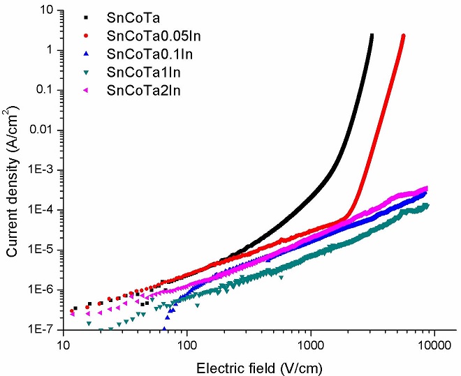
Results from electrical (J − E) measurements for the set of specimens with all experimental compositions and for reference materials, are shown in Fig. 7. As can be seen in this figure, only the reference material and the specimen with 0.05 mol. % In2O3 exhibited non-linear or varistor behavior. Apparently, above 0.05 mol % InO2, the specimens show a highly resistive performance, behaving like dielectric materials. This tendency can be observed in the values of measured mean grain size (l g ) shown in column 5 of Table I. Therefore, it can be stated that as the In2O3 content increases there is a decrease in grain size and an increase in the breakdown voltage.
4. Conclusions
In this work the effect of In2O3 additions on the microstructure, physical and electrical properties of the SnO2-Co3O4Ta2O5 ceramic system was investigated. Because the effect of In2O3 has been studied typically at low levels, special attention has been paid to the effect of high levels (1 and 2 mol % In2O3) in the ceramics. Results show that up to 0.1 mol % In2O3, an increase of indium oxide content is correlated with grain size reduction and an increase of the nonlinearity coefficient (α) and breakdown voltage (E B ), producing an augmentation by a factor of 2 in the nonlinearity coefficient and an increment by a factor of 8 in the breakdown voltage. For In2O3 contents above 0.05 % mol the ceramic samples behave like dielectrics. Additionally, a high content of In2O3 may be responsible of promoting the formation of a SnO2 habitus on the surface of samples.

