


 nueva página del texto (beta)
 Inglés (pdf)
 Artículo en XML
 Referencias del artículo
 Enviar artículo por email
 Citado por SciELO
  Similares en
SciELO
Similares en
SciELO 
 Permalink
1. Introduction
The development of high mobility thin-film transistors (TFTs) is a highly demanded research topic, in order to meet the requirements for advanced applications such as driving circuits, nonvolatile memory devices and flexible integrated circuits [1, 2]. Inorganic oxide semiconductors such as zinc oxide (ZnO) or Indium-Gallium Zinc Oxide (IGZO) are considered an important alternative to the mature amorphous silicon TFT technology mainly to their high performance and low temperature deposition [1, 2]. However, the research of new materials with higher electron mobilities to be considered for TFTs applications is under development.
Recently, zinc nitride (Zn3N2) has been explored in order to be used in TFTs due to the high Hall electron mobilities reported for films deposited at low temperatures [3-6]. Previous reports, demonstrated transistor performance for Zn3N2 films deposited at room temperature, achieving electron mobilities above 2 cm2/Vs [7]. Although this is promising, it is necessary to increase the electron mobility in order to achieve comparable values to those reported for other high mobility TFTs technologies.
In this work, high mobility TFTs based on Zn3N2 deposited at room temperature using spin-on glass (SOG) as gate dielectric are presented. The inverted coplanar structure was used for the TFTs. Furthermore, n-type metaloxide-semiconductor (MOS) capacitors were fabricated and characterized to evaluate the dielectric characteristics of the SOG film. The maximum temperature used for the preparation of the gate dielectric was 200◦C, whereas the aluminum source/drain electrodes were deposited at room temperature by DC sputtering. This fabrication conditions are compatible with the development of flexible TFTs, as previously demonstrated [8].
2. Experiment
The n-type MOS capacitors were fabricated using n-type silicon wafers (Phosphorous, 1-10 Ωcm). The dielectric consisted of a SOG layer spin-coated at 3000 rpm for 30 s and cured at 200oC for 1.5 h. The SOG precursor solution was prepared from 33% of LSF47-SOG solution diluted in 66% LSFD1 diluent (Filmtronics Inc. USA). The thickness of the SOG film was 85 nm and was corroborated with a profilometer. Fluorine tin oxide (FTO) layers with a F/Sn compositional ratio of 0.52 were deposited by ultrasonic spray pyrolysis to fabricate top and bottom electrodes using a shadow mask. The top electrodes have an area of 0.012 cm2.
The inverted coplanar Zn3N2 TFTs were fabricated atop heavily doped p-type silicon wafers, which were used as gate electrode. As gate dielectric, SOG was spin-coated at 3000 rpm for 30 s and cured at 200oC for 1.5 h. The thickness of the SOG film was 85 nm, same as for MOS capacitors. After that, 100 nm-thick aluminum was plasma sputtered at room temperature and patterned as source/drain electrodes by wet etching. The working pressure was 10−2 mbar with a DC power of 250 W. Finally, a 20 nm-thick film was plasma sputtered at room temperature followed by a 20 nmthick ZnO film as passivation layer. The plasma discharge was induced between a 4-in. circular Zn target (99.995% purity) and the substrate, using 30 sccm flux of Nitrogen gas (99.999%) with a radio frequency power of 100 W. The working pressure was 10−2 mbar. The passivation ZnO thin film was plasma sputtered at room temperature from the same Zn target using 50 sccm flux of Oxygen gas (99.999%) and a radio frequency power of 250 W. The plasma sputtered system used was the A450 ALCATEL. The Zn3N2TFTs was a dimension W/L= 124/8 µm. The electrical characteristics were measured using a Keithley-4200 Semiconductor Characterization System, under dark conditions, air ambient, and room temperature.
3. Results and discussion
Figure 1 shows the capacitance-voltage characteristics at 100 kHz for the n-type MOS capacitors using the SOG films cured at 200oC. The characteristic of the capacitor shows a well-defined accumulation region with very low hysteresis. This region is due to an accumulation of electrons at the dielectric-semiconductor interface. The device works as a parallel-plate capacitor, where the capacitance is equal to the oxide capacitance. Also, the flat band voltage is close to 0.5 V which indicates that a high-quality dielectricsemiconductor interface is achieved regardless of the low curing temperature. This is important to obtain high uniformity in the electrical characteristics of the Zn3N2 TFTs, since the gate dielectric determines the charge density, threshold voltage and leakage current. The very low hysteresis exhibited in the MOS capacitors may assures a low charge-trapping rate at the dielectric-semiconductor interface in TFTs using SOG films as gate dielectric.
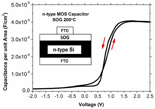
FIGURE 1 Capacitance-voltage characteristics at 100 kHz for the n-type MOS capacitors using SOG as gate dielectric. Inset: schematic cross section of the MOS capacitors. The well-defined accumulation region with very low hysteresis indicates a highquality dielectric-semiconductor interface.
Figure 2 shows the current density of the n-type MOS capacitors. The values of current density are reliable for semiconductor devices. The MOS capacitor does not exhibit a breakdown for voltages applied up to 60 V. This reliable current density assures a low gate leakage current in the Zn3N2 TFTs, which improves the TFT performance [9].
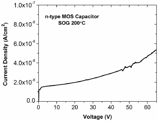
FIGURE 2 Current density characteristic of the n-type MOS capacitors using SOG as gate dielectric. The value of the current density assures a low gate leakage current in the Zn3N2 TFTs.
Figure 3 shows the frequency dependence of the n-type MOS capacitors using SOG as gate dielectric. The accumulation capacitance exhibits a good stability at low and high frequencies regardless of the low curing temperature. However, it can be observed a slight frequency dependence (also called frequency dispersion) which is well-known and is expected for MOS capacitors. The above results confirm the potential to use SOG films as gate dielectric in high performance TFTs.
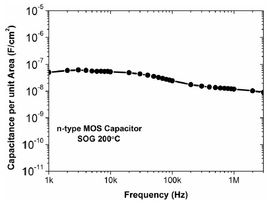
FIGURE 3 Frequency dependence of the n-type MOS capacitors using SOG as gate dielectric. The accumulation capacitance exhibits a good stability at low and high frequencies regardless of the low curing temperature.
Figure 4 shows the transfer characteristics of the inverted coplanar Zn3N2 based TFTs. The Zn3N2 TFTs work at enhancement mode. The devices exhibit an on/off-current ratio of 106 and a subthreshold slope of 0.88 V/decade. Typically, in TFTs, the subthreshold slope is dependent on the trap density in the active layer (NT) and at the dielectricsemiconductor interface (D it ). The subthreshold slope can be approximated as the following equation [10]:
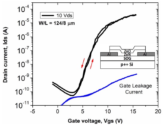
FIGURE 4 Transfer characteristics of the Zn3N2TFTs. Inset: schematic cross section of the TFTs. The devices exhibit an on/offcurrent ratio of 106, a subthreshold slope of 0.88 V/decade, an extracted field-effect mobility of 15.8 cm2/Vs and V T of 6.5 V.
where q is the electron charge, K B is the Boltzmann constant, T is the absolute temperature, T ZnN is the Zn3N2 thickness and Cox is the capacitance per unit area of the gate dielectric. If N T or D it is separately set to zero, the respective maximum values of N T and Dit are obtained. The N T and Dit values for Zn3N2 TFTs were 1.83×1018 cm−3eV−1 and 3.66 × 1012 cm−2eV−1, respectively. As far as the authors know, N T and D it values have been not reported for Zn3N2 TFTs. However, these values are lower than those reported for ZnO and AZO TFTs [10,11].
The electron field-effect mobility was extracted using the Eq. (2) of the TFTs in the saturation regime [12].
where µ FE is the field-effect mobility, C ox is the capacitance per unit area of the gate dielectric (4 × 10⁻⁸ F/cm2), W and L are the channel width and the length, respectively, and VT is the threshold voltage. The extracted field-effect mobility was 15.8 cm2/Vs and VT was 6.5 V. This is consistent for at least 10 measured TFTs. The gate leakage current was ∼ 1 × 10⁻⁹ A at 15 Vgs, which is several orders of magnitude lower than the drain current. Therefore, the gate leakage does not affect the electrical performance of the Zn3N2TFTs.
Figure 5 shows the output characteristics of the Zn3N2 TFTs. The devices exhibit well defined linear and saturation regimes. However, it can be seen slight current crowding effects at very low Vds values. Although the channel length is very small (8 µm), the output characteristics do not exhibit short channel effects. On the other hand, it has been reported that Zn3N2 films easily oxidized in air, and this leads to some inconsistences in the film properties [3,13,14]. Previous works [6,8] reported the passivation with ZnO which reduces the oxidation process of the Zn3N2 films. This leaves the properties of the Zn3N2 film unaffected and explains the high electron mobility achieved. Further research is necessary to optimize the drain/source contact regions in order to reach a higher electron mobility.
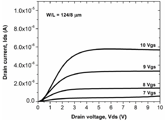
FIGURE 5 Output characteristics of the Zn3N2 TFTs. The devices exhibit well defined linear and saturation regimes, and do not exhibit short channel effects.
These results show an improved performance compared with those reported in other TFTs technologies [15-22]. In [16], mobilities of 0.83 cm2/Vs for room temperature sputtered Ga-SnO TFTs were reported. In [17], electron mobilities close to 10 cm2/Vs were reported for boron indium oxide TFTs with thermal annealing of 200oC. In [18], electron mobilities below 10 cm2/Vs were reported for Li-N doped ZnO TFT annealed at 300oC. Also, an electron mobility of 8 cm2/Vs was reported for room temperature IGZO TFTs [19]. In [20], the electron mobility reported was close to 10 cm2/Vs for zinc oxynitride TFTs deposited at 50oC, and annealed at 350oC. The electrical performance obtained is better than that reported previously in Zn3N2TFTs on silicon wafers [7]. The improvement in the electrical characteristics is due to an optimized source/drain contacts fabrication in order to improve the metal-semiconductor interface. To the best of our knowledge, the electrical characteristics obtained are among the highest electrical performance reported for room temperature deposited active layers based TFTs [21-22].
The above results confirm the feasibility of use Zn3N2films in TFTs to enable novel applications in the near future and to be a real alternative to silicon technology.
4. Conclusions
In this work, high mobility TFTs based on Zn3N2 sputtered at room temperature using SOG as gate dielectric are presented. The devices exhibit an on/off-current ratio of 106, a subthreshold slope of 0.88 V/decade and an extracted fieldeffect mobility of 15.8 cm2/Vs. To the best of our knowledge, the electrical characteristics obtained are among the highest electrical performance reported for Zn3N2 TFTs and are considerably better than those reported in other TFTs technologies using active layers deposited at room temperature. The gate leakage current is several orders of magnitude lower than the drain current, which does not affect the electrical performance of the Zn3N2 TFTs. The output characteristics do not exhibit short channel effects at channel lengths of 8 µm.

