SciELO - Scientific Electronic Library Online

 
vol.64 número6A comparative analysis of the RC circuit with local and non-local fractional derivativesLocal available quantum correlations for Bell diagonal states and Markovian decoherence índice de autoresíndice de assuntospesquisa de artigos
Home Pagelista alfabética de periódicos  

Serviços Personalizados

Journal

Artigo

Indicadores

Links relacionados

  • Não possue artigos similaresSimilares em SciELO

Compartilhar


Revista mexicana de física

versão impressa ISSN 0035-001X

Rev. mex. fis. vol.64 no.6 México Nov./Dez. 2018  Epub 05-Nov-2019

https://doi.org/10.31349/revmexfis.64.655 

Research

Determination of the barrier height of Pt-Ir Schottky nano-contacts on Al-doped ZnO thin films by conductive Atomic Force Microscopy

J. Eduardo-River L.a 

N. Muñoz-Aguirrea  c 

G. Juliana Gutiérrez-Paredesa 

P.A. Tamayo-Mezaa 

Alejandro A. Zapataa 

L. Martínez-Pérezb  c 

a Instituto Politécnico Nacional, Sección de Estudios de Posgrado e Investigación, Escuela Superior de Ingeniería Mecánica y Eléctrica-UA. Av. Granjas, N± 682, Colonia Santa Catarina. Del. Azcapotzalco, CP. 02250, CDMX, México.

b Unidad Profesional Interdisciplinaria en Ingeniería y Tecnologías Avanzadas, Instituto Politécnico Nacional, Av. IPN, No. 2580, Col. Barrio La Laguna, Tecomán, 07340, CDMX, México.

c Departamento de Física del Centro de Investigación y de Estudios Avanzados del IPN, 07351 Ciudad de México, México. (Affiliation of sabatic year 2017-2018).


Abstract

By means of the I-V characteristics measured at room temperature, the height of the Schottky barrier established by the conductive Pt-Ir tip of an Atomic Force Microscope on the aluminum doped ZnO thin films were estimated in the range of 0.58-0.64 eV. The ideality factors were in the range of 2.11-1.39, respectively. These values are in accordance with those reported by other authors that measured the height of the Pt Schottky barrier on ZnO by means of several methods. The procedure detailed in this work suggests that the scanning time for obtaining I-V Schottky characteristics is of the order of 2 ms.

Keywords: Schottky barrier height; conductive AFM; I-V Schottky characteristics; Pt Schottky nano-contact on ZnO thin films; electrical properties at nanoscale level

PACS: 73.61.Jc; 73.30.+y; 72.20.-I; 07.79.Lh

1. Introduction

Aluminum doped zinc oxide (AZO) thin films have many important applications, principally as sensing and optoelectronic material [1]. Another interesting application is related to its use as transparent conductor [1,2] in solar cell technology. AZO films have some advantages such as higher transmittance even at near infrared wavelengths than ITO [1]. Then, the electrical characterization of someone heterojunction formed with AZO films is of great importance. One of this heterojunction is the Shottky barrier formed with a metal contact as for instance the conductive tip of an Atomic Force Microscope scanning on its surface. Few works are related with the AZO heterojunctions [3] and few talk about of the Schottky nano-contact formed with an AFM tip [4]. The leakage current of a Schottky contact strongly depends on the barrier height. A Schottky barrier of a metal-semiconductor interface must be high in order to reduce the leakage current. Then, it is also very important to research the barrier height of the Schottky nano-contact on AZO thin films by means of the C-AFM technique as is made in this work.

On the other hand, it is well known that Atomic Force Microscopy (AFM) is an important tool in the nanotechnology as for example in the investigation of electrical properties by means of Scanning Tunneling Microscopy or the conductive AFM technique [5-7]. The conductive Atomic Force Microscopy (C-AFM) technique has been widely used to measure the surface electrical current of different materials such as conductors, semiconductors, dielectric or even biological materials [8-14]. Werner Frammelsberger et al.[8] reported electrical measurements of SiO2 thin films using C-AFM technique. Kevin D. O’Neil et al.[9] reported electrical conductivity of uranium oxide using C-AFM as well. Jeffrey M. Mativetsky et al. [10] reported molecular junction studies by means of conductive Atomic Force Microscopy. Liam S. C. Pingree et al. [11] reported Electrical Scanning Probe Microscopy on active organic electronic devices. Miłosz Grodzicki et al. [12] reported C-AFM measurements of Shottky barriers on metal-semiconductor heterostructures. N. Muñoz-Aguirre et al. [13] has shown images of the surface of ZnO thin films by means of C-AFM and recently Fanny Hauquier et al. [14] reported electrical properties of graphene sheets. Specially attention is directed to the Schottky barrier conformed by the conductor-semiconductor union [15-21] since in the C-AFM technique a tip coated by a metal alloy of Pt-Ir is principally used. For the first time in 1874 Braun studied such heterostructure, however the first accepted theory was developed by Schottky in 1930 [22]. Recently, S.J. Young et al. [20] applied the Pd/ZnO Schottky barrier as an ultraviolet photodetector and C. Weichsel et al. [21] developed Pd/ZnO Schottky diodes for hydrogen gas sensing. It is important to mention that the Modern Atomic Force Microscopes have relevant advantages since can measure spectroscopic I-V characteristics at different points of the sample surface [13]. In relation to the last mentioned reports, few authors detail the procedure in order to obtain their electrical characterizations by means of C-AFM. Therefore in this work, a detailed procedure for measure the I-V characteristic by the C-AFM technique and guarantee reliable results is proposed.

2. Materials and methods

2.1. Synthesis of the samples

As was detailed in a previous work [2], an ultrasonic spray pyrolysis deposition system was used. Source solutions of 0.3032 molar concentrations of zinc acetylacetonate and 10% of aluminum acetylacetonate (Sigma Aldrich) dissolved in N, N-dimethylformamide (N,N-DMF) (Mallinckrodt) were prepared. A mist from the materials source solution is produced by means of an ultrasonic generator operated at 0.8 MHz. A high purity air at flow rate of approximately 10 l/min was used as the carrier gas in order to transport the mist to the surface of the substrate during five minutes. A molten tin bath was the substrate heater. Substrates of Corning 7059 glass which were carefully cleaned using a well-known cleaning procedure [23] were used. Simultaneously, substrates of stainless steel discs were used as well. The depositions were carried out at substrate temperatures of 500C. Five percent of aluminum was finally incorporated to the ZnO thin films.

2.2. Atomic Force Microscopy experimental configuration

The electrical characterization was performed using a JSPM-5200 microscope (JEOL). In order to guarantee a good electrical contact of the AZO sample, these were deposited on stainless steel substrates, as specified in Sec. 2.1. Then, metal-semiconductor unions or Schottky nano-contacts were formed with the Pt-Ir conductive probe place on the surface of the semiconductor thin solid film as is shown in Fig. 1.

Figure 1 Scheme of the experimental configuration of the conductive AFM technique.  

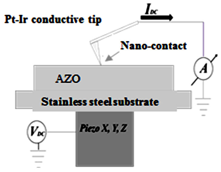
As was mentioned above, for the characterization of this nano-contact the conductive AFM method in contact mode [8-14] was used. The used tip was the SCM-PIT model (BRUKER) which has a nominal spring constant of kn=2.8 N/m and has a metallic coating of Platinum-Iridium of 20 nm thickness. The average radio of the tip curvature is in the order of 20 nm as is shown in Fig. 2.

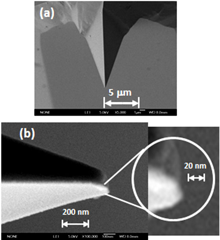
Figure 2 Scanning Electron Microscopy image of the Pt-Ir coated tip used in the experiments; (a) front view, (b) close up of the lateral view showing the curvature of the tip.  

Now, using the method proposed by Sader [33], we proceeded to estimate the value of the constant “k” of the beam, Eq. (1):

kexp=ρω2M0. (1)

Where, kexp-experimental constant of the beam in (N/m); ρ-NiSi density equals 3440 kg/m3; ω-frequency of the beam in (Hz); Mo-Normalized effective mass equal to 0.2427 for l/w>5 [33]; -Beam volume in (m3).

The volume of the beam can be determined by means of Eq. (2):

=wlt (2)

Where w-width of the beam equal to 28 μm [34]; l-length of beam equal to 225 μm [34]; t- Beam thickness equal to 2.75 μm [34].

The frequency of the “ω” beam was measured using the AFM, and the measurement was made under environmental conditions. The result of the measurement can be seen in Fig. 3.

Figure 3 Results of the measurement of the frequency “ω”.  

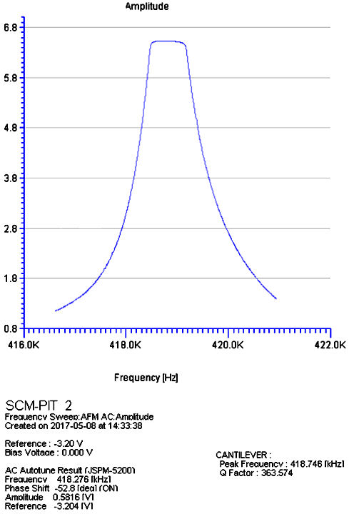
From Fig. 3, the value of ω=418.746 kHz is observed. With the aforementioned data it is possible to estimate the value of kexp=2.54 N/m, taking for this case that l/w=225/28=8, and therefore, the value of M0 can be taken for the estimation of kexp. As can be seen in this calculation, the spring constant of the beam is a value very close to the nominal value reported by the manufacturer, kexpkn, with a difference of 0.26, Bruker, Probes and Accessories, Pg. 111.2.3.

3. Methodology of the conductive AFM

Before taking the electrical measurements of the AZO thin films, it was necessary to calibrate the conductive mode of the microscope since the I-V curve depends drastically on the microscope parameters such as magnitude of the applied tip force [11,24], time of scanning (clock), the control circuit gains (Pre Amp Gain and Line Current), type of ramp and voltage range, among others [25]. Many authors do not report the calibration of theirs measurements due to the difficulty of obtaining the optimal software parameters of the microscope. In this section, we establish a methodology for optimizing such parameters and set the best experimental conditions in order to chracterize the samples. We think that the most important parameter is the magnitude of the applied tip force. In order to adjust such parameter, a metallic copper slide was used and also knowing that its I-V characteristics satisfies the Ohm’s law. In 
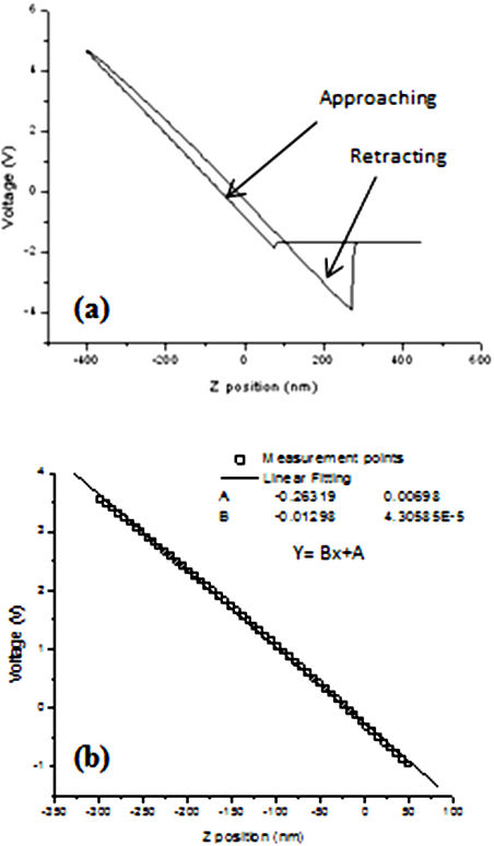
the same configuration of Fig. 1, over the steel substrate a copper slide sample was placed. Then, the force curve (FC) was measured using the standard contact mode of the Microscope as is shown in Fig. 4a. After that, a linear fitting in the retraction region was performed (See Fig. 4b) resulting a value of the slope curve equals to -0.01298 V/nm. According to the operation manual of the microscope [25], with the reciproc of the absolute value of the slope the sensibility parameter was calculated, resulting in 77.0416 nm/V. Introducing in Eq. (3), the sensibility value (a), the elastic constant (k) and the reference voltage V0=-2 V, the applied tip force as a function of the voltage was obtained [25]. A value of the tip contact force equals to -249.820 nN, which was calculated for the Microscope Software at the minimum of the force curve in the approaching zone, guarantees a real physical contact and it was fixed for obtaining the I-V curves.

F=ka(V-V0) (3)

Figure 4 (a) Measured Force Curve. (b) Linear fitting in the retracting zone  

After the force was determined, the measurements of the I-V characteristics were performed adjusting the electric control parameters using the same copper slide. In Fig. 5, it is shown the I-V curve in the range of -0.5 to 0.5 V (Fig. 5a) and from -1 to 1 V (Fig. 5b). These curves were measured under the following parameters conditions; Clock=66.67μs, Force=-249.820 nN, Pre-AmpGain=1.00 V/nA and LineCurrent=1 K.

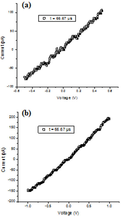
Figure 5 I-V characteristics for copper slides measured from (a) -0.5 to 0.5 V and (b) -1 to 1 V at the scanning time of 66.67 μs.  

From Fig. 5, it can be observed a linear behavoir characteristic of the Ohm’s law for a metal such as copper. It can be mentioned that the behavoir of the I-V characteristics is quite sensitive to the scanning time (Clock), however if the if the Force, Gains and Line Current parameters are fixed the measurements are clearly reproducible as it is shown by the plots in Fig. 4, for two different scanning times. Using the obtained Force and Line Current for the copper sample, and the Pre-AmpGain=0.1 V/nA as suggested by the Microscope manual [25] for semiconductor materials, four I-V characteristics for monocristalline silicon slides in the range of -1 to 1 V were measured for different scanning times. The results are shown in Fig. 6, for times in the interval of 66.67 μs to 2.0 ms.

Figure 6 I-V curves of silicon slides from -1 to 1 V at different scanning times.  

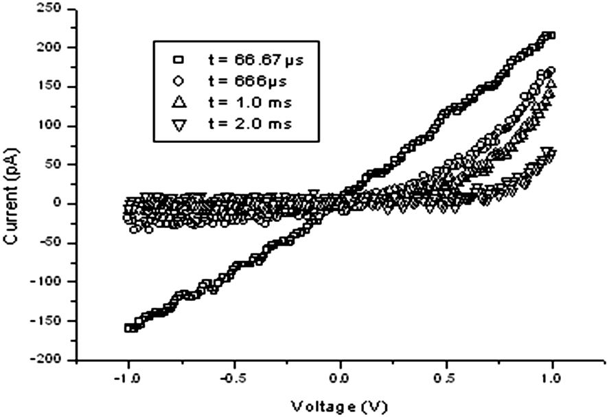
It is observed that for short scanning times of the order of μs the behavoir of two of the plots do not correspond to the union metal-semiconductor (Schottky barrier). However, for times in the order of 1 ms the Schottky barrier behavoir starts and it is clearly observed as is shown in Fig. 7a. For larger times the total rectification takes place as shown in Fig. 7b. For fast measurements (times of μs), a real contact of the tip on the sample surface does not take place and the tunneling current should also be important as the thermionic current as was considered by Milosz Grodzicki et al.[12] and S. ZhengZheng et al.[26]. Therefore, the optimal conditions to obtain a good Schottky effect is to measure the I-V curves at scanning times higher than 2 ms.

Figure 7 I-V characteristics for scanning times of 1 ms (a) and 2 ms (b). For 2 ms the total rectified Schottky condition is showed for the reverse bias voltage. The lines are the thermionic theoretical model [22,24].  

4. Results and discussion

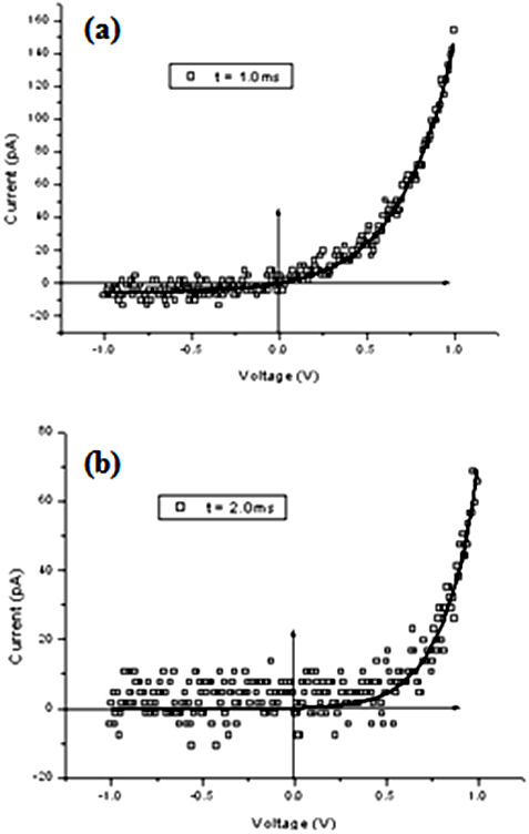
As shown in Fig. 8, topography and linear current images of the surface of the AZO thin films were taken at a scan area of 4×4 μm and an applied voltage of -60.340 V. After that, I-V curves at different points on the AZO surface as marked in Fig. 8a, were measured with a scanning time of 2 ms. The fitting of the theory to the I-V measured data was performed by Eqs. (4) and (5) which corresponds to the thermionic charge transport model [22,24].

Figure 8 Topography (a) and their corresponding linear current image (b) of the surface of the AZO thin films. The scanned area is 4×4 μm.  

I=I0[expeVnkBT-1]. (4)

With

I0=AR*T2[exp-eϕBkBT], (5)

Where -n is the ideality factor, I0- is the reverse bias current, e- is the electron charge, kB- is the Boltzmann’s constant, A- is the area of the nano-contact, R*- the Richarson’s constant and T- is the absolute temperature. In this case the area of the nano-contact depends on the curvature of the tip, which was in the order of 20 nm (See Fig. 2b) and can be approximated to a circle of the same diameter with an approximated area equal to A=π×10-12cm2.

Moreover, the value of KBT/e was 0.023 eV, the theoretical Richardson’s constant value for silicon material was R*=112 A cm-2K-2 [27] and for n-ZnO was R*=32A cm-2K-2 [15], T was considered as 300 K. Figure 9 shows two I-V curves for the x1, x2 positions and their corresponding fittings. The thermionic theoretical model has an excellent fitting with respect to the experimental data as can also be observed from the same figure. The red circles plot is the experimental data and the black triangles are the fitting, the correlation coefficients for all curves were 0.9994. The results for five marked points in Fig. 7a are summarized in the Table I. From this table, it can be established that the Schottky barrier height ΦB at the nanoscale level depends principally on the area of the real contact between the tip and the surface roughness.

Figure 9 I-V Schottky characteristics shown for two different points at the surface.  

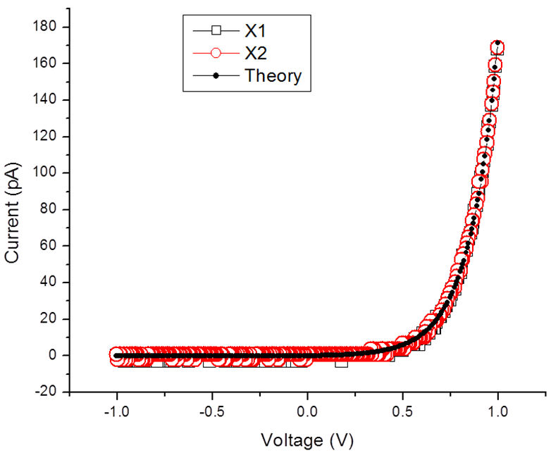
Table I Summary of the Schottky parameters results by means of the thermionic fitting model, measurement with C-AFM, effective area A=π×10-12 cm 2

Position Reversecurrent I0 (A) Ideality factor (n) Schottky barrierheight (eV)
x 1 2 .05 × 10 −16 1.39 0.64
x 2 2 .79 × 10 −16 1.50 0.63
x 3 8 .15 × 10 −16 1.80 0.60
x 4 1 .09 × 10 −15 1.91 0.59
x 5 1 .71 × 10 −15 2.11 0.58

It is also important to mention that the n ideality factor was an adjustable parameter in the fitting which should be related with this real nano-contact. From Table I, it can be observed that the Schottky barrier height is in the range of 0.58-0.64 eV and the ideality factors n are in the range of 2.11-1.39, respectively.

Since the 1965 year, a value of 0.75 eV of the Pt-ZnO barrier height was reported by Mead [28], obtained using internal photoemission yield spectroscopy. K. Ip et al.[15], reported a value of 0.61±0.04 eV for the height of the Schottky barrier of traditional Pt contacts on ZnO thin films. These values were obtained at room temperature from current-voltage curve measurements with an ideality factor of 1.7. Y. W. Heo et al.[16], reported a value of n factor equal to 1.1 for ZnO nanowires. Sang-Ho Kim et al.[18], using capacitance-voltage curves reported ideality factors of 1.51, and 0.79 eV of the height Schottky barriers for Pt contacts on ZnO sulfide treated single crystals, and 0.89 to 0.93 eV for ZnO hydrogen peroxide solution treated [29]. Also Saraswatchi et al. [31], report the union Pt-ZnO equal to 0.43 eV at a temperature of 300 K and an effective area of 2.8×10⁻¹¹ cm2. This area is similar to our work.

In relation to contacts different to Pt, the Schottky barrier heights of 0.65-0.70 eV and ideality factors in the range of 1.6-1.8 for Au and Ag with contacts on ZnO were reported by A. Y. Polyakov et al. [17], measured by means of capacitance-voltage curves. Also, H. Wenckstern, et al., [19] reported a mean barrier height of Pd Schottky and contacts on ZnO thin films as 1.16±0.04 eV measured by means of temperature-dependent current-voltage and capacitance-voltage curves. On the other hand, Sangku et al. [32], study on the electrical properties of Pt/CdSe nanojunctions using connected Au islands, reveals that a Schottky barrier is formed at the interface between Pt and CdSe, and found that the Schottky barrier height and the ideality factor of an individual nanojunction are 0.41 eV and 9.9, respectively. Our results differ with the reported in [17,19,32], because this uses another type of union.

As was mentioned in the introduction, there are few works related to the measurement of Schottky barrier height on ZnO or AZO thin films by means of C-AFM. For instance, W. I. Park et al. [30] reported measurements for ZnO nanorods with Au coating contact tips by means of current-sensing Atomic Force Microscopy (CS-AFM). Recently, Periasamy and P. Chakrabarti [24] measured a ZnO nanoneedle array with Pd coating contact tips by means of CS-AFM resulting in 0.76 eV for the Schottky barrier height and 7.41 the value of the ideality factor. It can be noted the large value of the ideality factor, however it is in accordance with the values reported in this paper (see Table I). During I-V measurements in Ref. 24, a constant normal force of 15 nN was kept between the tip and ZnO nanoneedle array. In this work, an applied higher normal force in the order of 249.820 nN of absolute value, as was determined from the calibration of the microscope in the Sec. 2.3, is suggested. Moreover, it must be taken into account the scanning time of the order of 2 ms in order to obtain smaller reverse current as shown in Fig. 8. These suggestions should improve the measurements of the Schottky height barrier and the ideality factor. Specifically for Pt nano-contacts, Shao ZhengZheng et al. [26] reported an ideality factor of 3.2 by means of C-AFM measurements that is in accordance with the values reported in this work (see Table I).

Is important to make mention that in this experimental work, the effect of the relative humidity was not considered on the made electrical measurements and therefore on the height Schottky barrier estimate. However, this work proposes considering humidity as one more factor that affects the deviation of the ideal factor “n” and, consequently, in how the relative humidity affects the size of the Schottky barrier. Finally, to improve the results obtained, it is suggested to perform electrical measurements in vacuum and quantify the effect that environmental relative humidity exerts on the size of the Schottky barrier. In addition, develop a thermionic model different from the conventional one that considers the influence of environmental relative humidity on the size of the Schottky barrier.

5. Conclusions

Values of the height of the Schottky barrier on Aluminum-doped ZnO thin films were estimated using the conductive AFM technique. The estimated values were in the range of 0.58-0.64 eV as those reported in the literature. It was also showed that scanning times of 2 ms or longer must be used in order to achieve good measurements of the I-V characteristics when using the conductive AFM technique. It is also concluded that this AFM alternative electrical-electronic measurement methodology is promising for studies at the nanoscale level.

Acknowledgments

This work was supported by Instituto Politécnico Nacional, México, with the projects number SIP20162072, SIP20141031 and 20140956. The authors also would like to acknowledge the technical assistance of Ing. Ana Berta Soto in obtaining the SEM images of the AFM tip and QFB. Miss Marcela Guerrero, both from the Physics Department of CINVESTAV-IPN, México.

References

1 H. Kim et al., Appl. Phys. Lett. 76 (2000) 259. [ Links ]

2 L. Martínez Pérez, M. Aguilar-Frutis, O. Zelaya-Angel and N. Muñoz Aguirre, Phys. Stat. Solidi a 203 (2006) 2411-2417. [ Links ]

3 J. K. Sheu, M. L. Lee, C. J. Tun, S. W. Lin, Appl. Phys. Lett. 88 (2006) 043506. [ Links ]

4 R. Jaramillo, S. Ramanathan, Solar Energy Materials & Solar Cells 95 (2011) 602-605. [ Links ]

5 S. Gauthier, C. Joachim, Scanning Probe Microscopy: Beyond the images, (Les Editions de Physique 1991). (ISBN 2-86883-178-8). [ Links ]

6 E. Meyer, Scanning Probe Microscopy: The Lab on a Tip, Springer-Verlag Berlin Heidelberg (New York 2004) (IBBN 3-540-43180-2). [ Links ]

7 R. Wiesendanger, Scanning Probe Microscopy and Spectroscopy Methods and Applications CAMBRIDGE UNIVERSITY PRESS (2004). (ISBN-13:9780521428477 | ISBN-10:0521428475). [ Links ]

8 W. Frammelsberger, G. Benstetter, J. Kiely, R. Stamp, Appl. Surf. Science 253 (2007) 3615-3626. [ Links ]

9 K. D. O’Neil, H. He, P. Keech, D. W. Shoesmith, O. A. Semenikhin Electroch. Commun. 10 (2008) 1805-1808. [ Links ]

10 J. M. Mativetsky, M. Palma, P. Samorì, Top. Curr. Chem. 285 (2008) 157-202. [ Links ]

11 L. S. C. Pingree, O. G. Reid and D. S. Ginger, Adv. Mater. 21 (2009) 19-28. [ Links ]

12 M. Grodzicki, S. Smolarek, P. Mazur, S. Zuber, A. Ciszewski Appl. Surf. Science 256 (2009) 1014-1018. [ Links ]

13 N. Muñoz-Aguirre, J.-E. Rivera-López, L. Martínez-Pérez and P. Tamayo-Meza, Mat. Sci. Forum 644 (2010) 109-112. [ Links ]

14 F. Hauquier et al., Appl. Surf. Science 258 (2012) 2920-2926. [ Links ]

15 K. Ip, Heo et al., Appl. Phys. Lett. 84 (2004) 2835. [ Links ]

16 Y. Heo, et al., Appl. Phys. Lett. 85 (2004) 3107. [ Links ]

17 A. Polyakov et al., Appl. Phys. Lett. 83 (2003) 1575. [ Links ]

18 K. Sang-Ho, K. Han-Ki and S. Tae-Yeon, Appl. Phys. Lett. 86 (2005) 022101. [ Links ]

19 H. Wenckstern, G. Biehne, R. A Rahman, H. Hochmuth, M. Lorenz, M. Grundmann Appl. Phys. Lett. 88 (2006) 092102. [ Links ]

20 S.J. Young, L.W. Ji, T.H. Fang, S.J. Chang, Y.K. Su, X.L. Du, Acta Materialia 55 (2007) 329. [ Links ]

21 C. Weichsel, O. Pagni and A. W. R. Leitch, Semicond. Sci. Technol. 20 (2005) 840. [ Links ]

22 Dieter K. Schroder, Semiconductor Material and Device Characterization Third Edition, A John Wiley & Sons, Inc., Publication. [ Links ]

23 Micro concentrated cleaning solution, International Products, Burlington, N.J. (1999). [ Links ]

24 C. Periasamy, P. Chakrabarti, Current Appl. Phys. 11 (2011) 959-964. [ Links ]

25 JSPM-5200 Scanning Probe Microscope, Instructions JEOL Ltd. [ Links ]

26 S. ZhengZheng, Z. XueAo, W. XiaoFeng and C. ShengLi, Physics Mechanics & Astronomy 53 (2010) 64-67. [ Links ]

27 S. Chand and J. Kumar, Appl. Phys. A 63 (1996) 171-178. [ Links ]

28 C. A. Mead, Phys. Lett. 18 (1965) 218. [ Links ]

29 K. Sang-Ho , K. Han-Ki , S. Tae-Yeon , Appl. Phys. Lett. 86 (2005) 112101 - 112101-3. [ Links ]

30 W. I. Park, Gyu-Chul Yi, J. W. Kim and S. M. Park, Appl. Phys. Lett. 82 (2003) 4358. [ Links ]

31 Saraswathi Chirakkara, Palash Roy Choudhury, K. K. Nanda and S. B. Krupanidhi, Mater. Res. Express 3 (2016) 045023. [ Links ]

32 Sangku Kwon, Seon Joo Lee, Sun Mi Kim, Youngkeun Lee, Nanoscale, 7 (2015) 12297. [ Links ]

33 J. E. Sader, Review of scientific instruments 70 (1999). [ Links ]

34 Bruker, Probe Catalog (2012), AFM. [ Links ]

Received: April 22, 2018; Accepted: August 14, 2018

Creative Commons License This is an open-access article distributed under the terms of the Creative Commons Attribution License