SciELO - Scientific Electronic Library Online

 
vol.64 número6Electrical transport phenomena in nanostructured porous-silicon filmsCasimir energy in a bounded Gross-Neveu model índice de autoresíndice de materiabúsqueda de artículos
Home Pagelista alfabética de revistas  

Servicios Personalizados

Revista

Articulo

Indicadores

Links relacionados

  • No hay artículos similaresSimilares en SciELO

Compartir


Revista mexicana de física

versión impresa ISSN 0035-001X

Rev. mex. fis. vol.64 no.6 México nov./dic. 2018  Epub 05-Nov-2019

https://doi.org/10.31349/revmexfis.64.566 

Research

Modulation of argon pressure as an option to control transmittance and resistivity of ZnO:Al films deposited by DC magnetron sputtering: on the dark yellow films at 10-7 Torr base pressures

J.A. García-Valenzuelaa  b  * 

D. Cabrera-Germanb  c  ** 

M. Cota-Lealb  c 

G. Suárez-Camposb  c 

M. Martínez-Gilb  c 

F. Romo-Garcíab  d 

M.R. Baez-Gaxiolab 

M. Sotelo-Lermac 

J. Andreue  f 

J. Bertomeue  f 

a Departamento de Ingeniería Química y Metalurgia, Universidad de Sonora, Blvd. Luis Encinas Johnson y Calle Rosales S/N, Col. Centro, 83000, Hermosillo, Sonora, Mexico.

b SMARTER-Lab Nucleus for Research & Divulgation, A.C., Blvd. Eusebio Francisco Kino No. 848, Local 6, Col. Pitic, 83150, Hermosillo, Sonora, Mexico.

c Departamento de Investigación en Polímeros y Materiales, Universidad de Sonora, Calle Rosales y Blvd. Luis Encinas Johnson S/N, Col. Centro, 83000, Hermosillo, Sonora, Mexico.

d Departamento de Física, Universidad de Sonora, Calle Rosales y Blvd. Luis Encinas Johnson S/N, Col. Centro, 83000, Hermosillo, Sonora, Mexico.

e Departamento de Física Aplicada, Universitat de Barcelona, Carrer de Martí i Franquès 1-11, 08028, Barcelona, Catalonia, Spain.

f Institut de Nanociµencia i Nanotecnologia, Universitat de Barcelona, Av. de Joan XXIII S/N, 08028, Barcelona, Catalonia, Spain.


Abstract

In a previous paper, we reported that thin films of ZnO:Al [aluminum-zinc oxide (AZO)] deposited after achieving a very low base pressure [from 4.0×10⁻⁷ Torr (5.6×10⁻⁵ Pa) to 5.7×10⁻⁷ Torr (7.6×10⁻⁵ Pa)] result dark yellow in color and are resistive. These are undesirable characteristics for the application of AZO thin films as front electrodes in solar cells. However, given the increasingly tendency in the acquisition of equipment that allows us to reach excellent vacuum levels, it is necessary to find the deposition conditions that lead to an improving of transmittance without greatly impacting the electrical properties of materials deposited after achieving these levels of vacuum. In this way, the present work is focused on AZO thin films deposited after achieving a very low base pressure value: 4.2×10⁻⁷ Torr (5.6×10⁻⁵ Pa). For this, we studied the effect of the variation of the oxygen volume percent in the argon/oxygen mixture (by maintaining the deposition pressure constant) and the effect of deposition pressure with only argon gas on the main properties of AZO thin films. The depositions were done at room temperature on glass substrates by direct-current magnetron sputtering with a power of 120 W (corresponding to a power density of 2.63 W/cm2). As a result, we found that the variation of deposition pressure with only argon gas is a good option for the control of optical and electrical properties, since the addition of oxygen, although improves transmittance, greatly impacts on the electrical properties. Furthermore, an interesting correlation was found between the optical and electrical properties and the chemical composition of the AZO films, the latter depending on the argon pressure (for this, a careful X-ray photoelectron spectroscopy analysis was performed). Also, the inverse relationship between crystallinity and deposition rate was confirmed, in which deposition rate inversely depends on argon pressure.

Keywords: Zinc oxide; transparent conductive oxide; sputter deposition; optical transmittance; electrical resistivity; argon pressure; base pressure

PACS: 72.80.Ey; 81.15.Cd; 88.40.H-

1. Introduction

The base pressure achieved prior to the sputtering deposition of a given material is an important parameter that strongly influences its final characteristics and properties [1-4]. The different vacuum levels achieved before the deposition process is especially important for transparent conductive oxides (TCOs) [5-10], where it is necessary a high transparency to the solar radiation (particularly to the radiation of interest for the device) and a very good conductivity to act as a front electrical contact for application in solar cells [11]. In this context, in a previous work [10] we studied the effect of the variation of this real deposition parameter on the electrical, optical, structural, and chemical characteristics and properties of thin films of Al-doped ZnO [ZnO:Al thin films, commonly known as aluminum-zinc oxide (AZO)], a material that is considered a good substitute of Sn-doped In2O3 [In2O3:Sn, commonly known as indium-tin oxide (ITO)].

The variation tendency of the relevant parameters studied in such a research is summarized in Fig. 1, which was divided into color zones according to the approximate appearance of the corresponding produced AZO thin films. We can observe there the existence of three main vacuum zones, each of which produced thin films that exhibited similar characteristics and properties. The first evidence of the existence of these three vacuum zones is the color of the deposited films, which is clearly different for each vacuum level, as shown in Fig. 2.

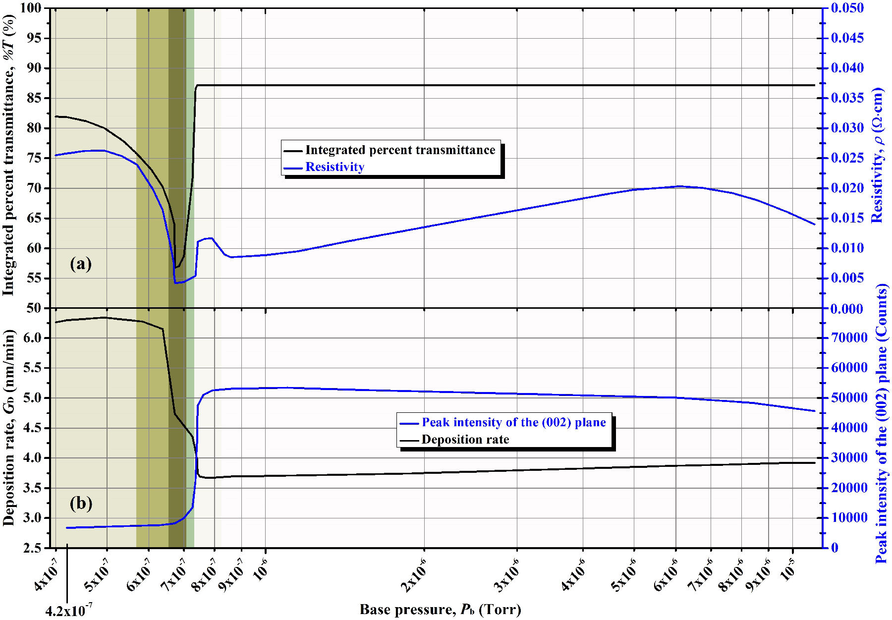
Figure 1 Variation tendency of the (a) integrated percent transmittance and resistivity, and (b) peak intensity of the (002) plane and deposition rate of the AZO thin films as functions of the base pressure achieved before the sputtering- deposition. See our previous work about the effect of base pressure [10].  

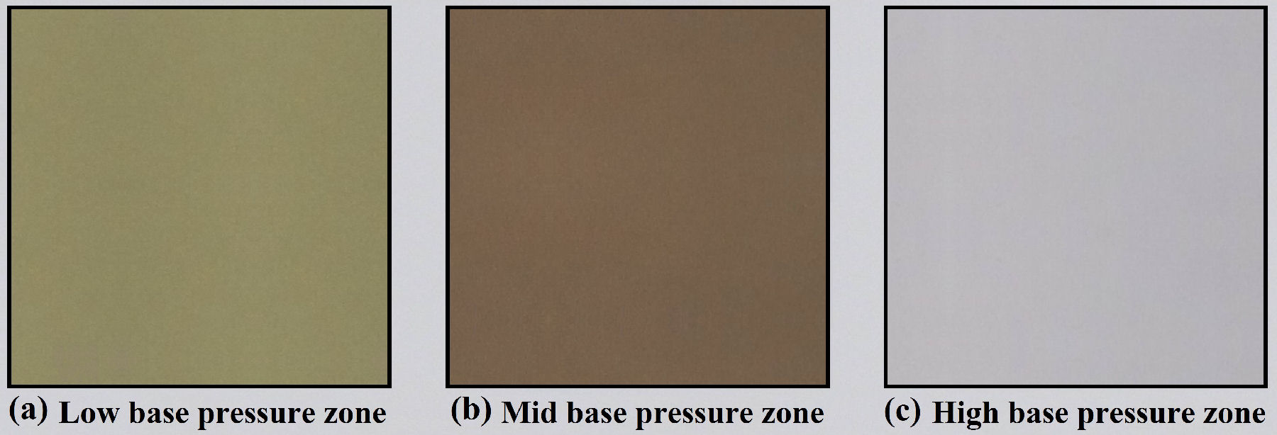
Figure 2 Digital photographs of the AZO thin films deposited after achieving representative base pressure values for each vacuum zone: (a) low base pressure zone [dark yellow zone: from 4.0×10⁻⁷ Torr (5.6×10⁻⁵ Pa) to 5.7×10⁻⁷ Torr (7.6×10⁻⁵Pa)], (b) mid base pressure zone [opaque zone: from 5.7×10⁻⁷ Torr (7.6×10⁻⁵ Pa) to 7.3×10⁻⁷ Torr (9.7×10⁻⁵ Pa)], and (c) high base pressure zone [transparent zone: from 7.3×10⁻⁷ Torr (9.7×10⁻⁵ Pa) to 1.1×10⁻⁵ Torr (1.5×10⁻³ Pa)]. The AZO thin films were placed on a white paper sheet, which is the background color of the figure. Although the background looks gray to the eye owing to the digitalization of the figure, it constitutes a reference for comparison: the AZO films deposited at higher base pressure (right) show a color similar to the background, indicating its high transparency. For more details, see our previous work about the effect of base pressure [10].  

Thus, values in the highest base pressure zone [>7.3×10⁻⁷ Torr (9.7×10⁻⁵ Pa), up to the studied value of 1.1×10⁻⁵ Torr (1.5×10⁻³ Pa)], that is, the bad vacuum levels, lead to good enough transparent and conductive AZO thin films. In this case, we found a wide range of high base pressure in which the residual gases are beneficial for the obtainment of good TCO properties. On the other hand, lower base pressure values, that is, good vacuum levels, lead to dark gray or brown AZO films with good conductivity in the narrow mid-vacuum interval from 7.3×10⁻⁷ Torr (9.7×10⁻⁵ Pa) to 5.7×10⁻⁷ Torr (7.6×10⁻⁵Pa), and dark yellow and resistive AZO thin films if the base pressure level is the best, that is, when the base pressure is lower than 5.7×10⁻⁷ Torr (7.6×10⁻⁵ Pa). Also, the thin films deposited after achieving this very good vacuum level are very unstable to the ambient air, becoming more resistive with the days.

From the previous results, we concluded that the presence of residual gases, at certain level, is beneficial for the properties of sputtering-deposited AZO thin films. In other words, good vacuum levels are not really necessary for TCOs, which is advantageous for the experimenter in saving costs of pumping systems and time in pumping process. Nevertheless, there is an increasingly tendency in the acquisition of better sputtering equipment with excellent pumping systems, thus allowing experimenters the opportunity to reach very good vacuum levels. However, as mentioned in the previous paragraphs, the best vacuum levels achieved by us lead to dark yellow and resistive AZO thin films (see Fig. 1 and Fig. 2), which are undesirable characteristics for TCOs.

With the above in mind, the present work aims to improve the transmittance of the AZO films deposited at room temperature after achieving a constant and very good vacuum level. Also, the deposition process for improving transmittance should not impact negatively on the electrical properties. To simplify the process, postdeposition treatments to improve transmittance are discarded. In this way, we studied the effect of the deposition parameters usually employed in the sputtering technique on the main properties of AZO thin films when a very good vacuum pressure is achieved prior to the sputtering-deposition: 4.2×10⁻⁷ Torr (5.6×10⁻⁵Pa). These deposition parameters are (a) the oxygen volume percent in the mixture of argon/oxygen, and (b) the deposition pressure with only argon gas. To properly explain the changes observed with the variation of these parameters, we characterized the deposited films by optical, electrical, structural, and chemical techniques, and each result was thoroughly discussed. Additionally, we tested the stability of the resulted films to the ambient air.

As a main result, we observed that the control of argon pressure, without the addition of oxygen, is better for providing a good compromise between transmittance and resistivity of the AZO samples deposited when a high vacuum level is achieved. Furthermore, an interesting correlation was found between the optical and electrical properties and the chemical composition of the AZO films, the latter depending on the argon pressure. Also, the inverse relationship between crystallinity and deposition rate was confirmed, in which deposition rate inversely depends on argon pressure. The overall results presented in this paper complement our previous work about the effect of base pressure on properties of AZO thin films [10], and therefore the reader is referred to such a work for more details.

2. Experimental details

2.1. Deposition methodology

The deposition equipment used for the present work was a commercial ATC-ORION 8 HV sputtering system from AJA International, Inc. It consisted of a 34.7 cm diameter and 39.8 cm height chamber with three different magnetron guns in a confocal geometry. In this configuration, the magnetron sputter guns, which can host targets of 7.62 cm (3 inch) in diameter, are tilted 3 and located 10 cm off-axis of the substrate.

The AZO thin films were deposited onto 5×5 cm2 1737F Corning glass substrates by direct current (DC) magnetron sputtering from a 99.99% purity ZnO:Al2O3 ceramic target composed of 98wt% ZnO and 2wt% Al2O3, which was purchased from Neyco. Before each deposition process, the glass substrate to be used was washed with deionized water and liquid soap, and then it was rinsed first with abundant deionized water and later with abundant isopropanol. Finally, the glass substrate was dried with nitrogen gas and placed on the holder-plate inside the sputtering chamber.

The distance from the center of the target to the center of the substrate was fixed at 18 cm, and a substrate rotation of 13 rpm was used to achieve good homogeneity during the material deposition. The films were deposited at room temperature with a DC power of 120 W, which corresponds, when divided by the target area (45.60 cm2), to a power density of 2.63 W/cm2. For the study of the effect of deposition pressure with solely argon gas (99.99%), the AZO thin films were obtained at 2.0 mTorr (0.27 Pa), 4.0 mTorr (0.53 Pa), 6.0 mTorr (0.80 Pa), and 8.0 mTorr (1.07 Pa), which were manually adjusted while maintaining the argon flow rate with a constant value of 20 sccm. For the study of the effect of addition of oxygen in the sputtering chamber, the oxygen volume percent values of 1.5%, 2.0%, and 2.5% were studied by varying the oxygen flow rate (details given in Table I), while the total deposition pressure was maintained in 4.0 mTorr (0.53 Pa), which was used in our previous work about the effect of the base pressure [10]. In all these cases, the deposition time was controlled to achieving AZO thin films with thickness of 260±20 nm.

Table I Flow rates of oxygen and argon employed for studying the effect of oxygen volume percent in the argon/oxygen mixture, by maintaining a total working pressure of 4.0 mTorr (0.53 Pa). 

Oxygen volume Oxygen flow Argon flow Total flow
percent (%) rate (sccm) rate (sccm) rate (sccm)
0.0 0.00 19.96 19.96
1.5 0.30 19.96 20.26
2.0 0.40 19.60 20.00
2.5 0.50 19.50 20.00

In the present study, the base pressure achieved prior to the sputtering-deposition was around 4.2×10⁻⁷ Torr (5.6×10⁻⁵ Pa) for all the cases, which was measured with a Granville-Phillips 274 Bayard-Alpert type ionization vacuum gauge, and it corresponds to a pumping time of 1000 min[10]. The vacuum was achieved using a dry primary pump and a high-vacuum turbomolecular pump (500 L/s). Also, it should be taken into account that no load lock chamber was used.

2.2 Characterization techniques

The thickness of all the deposited AZO thin films was measured with a Dektak 3030 profilometer, for which a simple lift-off technique was used on the films. The deposition rate, which was assumed constant along the film growing process, was calculated by dividing the measured thickness by the deposition time. The sheet resistance of the AZO thin films was measured by using a Jandel RM3 four-point probe system, and the resistivity was calculated by multiplying the measured thickness and the sheet resistance.

For the optical properties, the percent transmittance (%T) was recorded with a PerkinElmer Lambda 950 UV/Vis/NIR spectrometer using air as the reference, where the measurements were obtained with the AZO film facing the incident light. The measured %T was integrated in the interval from 400 to 1100 nm, which is the interval of interest for c-Si solar cells.

The structure of the deposited material was analyzed by means of a PANalytical X’Pert PRO MPD Alpha 1 powder X-ray diffractometer. The crystallite size was calculated from the X-ray diffraction (XRD) patterns by using the Scherrer equation [12-14]:

D=KλB2θcosθ, (1)

where D represents the mean dimension of the crystallite perpendicular to the diffraction plane; K is the shape factor, for which we employed the typical value of 0.9; λ is the wavelength of the X-ray used in the diffractometer, whose value is 0.15406 nm; B2θ is the full width at half maximum (FWHM) of the diffraction line in radians; and θ is the diffraction angle for the diffraction line position, for which the diffraction peak with the highest intensity was selected.

For the analysis of the chemical composition of the material, the AZO thin films were measured by X-ray photoelectron spectroscopy (XPS) by using a PHI Multitechnique system (from Physical Electronics) with a monochromatic X-ray source from the AlKα line with energy of 1486.8 eV. The measurements were obtained after an erosion treatment with an argon ion sputtering performed in the XPS system, and, due to the difficulty in identifying the Ar 2p3/2 peak (which must be located at about 241.83 eV, according to the average value of data compiled by Moulder et al. for argon implanted in silicon [15]), the binding energies of the recorded spectra were charge-corrected by referencing the center of the whole Ar 2p signal to 242.05 eV, according to our previous observation on argon implanted in sputtering-deposited Al2O3[16].

The quantitative analysis of the XPS spectra was done via peak-fitting using the AAnalyzer® software [17]. For an accurate experimental data reproduction, the peak-fitting procedure required the use of the active background approach[18,19], and the use of Voigt profiles. The Lorentzian widths were used as fixed constraints; for the Zn 2p and O 1s high-resolution spectra the widths were taken from data reported by one of the authors of the present work [20], while for the Al 2p core-level the widths are taken from data reported by Campbell & Papp [21]. Also, the theoretical branching ratio [22] was employed as a fixed parameter. The peak position, Gaussian broadening, spin-orbit splitting, and peak areas were considered as free variables and the fitting procedure allowed for their accurate determination [23] using a simultaneous fitting method [24].

The chemical composition analysis, on the other hand, was done using a method that takes into consideration physical parameters, that the films are homogeneous, and that the peak areas are proportional to their respective atomic densities according to the following equation [20,25-28]:

ρiIi,nldσi,nldΩAiλisinθ, (2)

where ρi is the atomic density of each chemical species in the material; Ii,nl is the intensity of the nl core-level for each element i; dσi,nl/dΩ is the differential photoelectric cross-section [29]; Ai corresponds to the efficiency of the spectrometer at the kinetic energy of the photoemission line for each element i; λi is the effective attenuation length; and θ is the photoelectron take-off angle. The input parameters are taken from values reported elsewhere [30-32].

3. Results and discussion

If a TCO thin film that is deposited by sputtering under certain conditions results with a low transmittance, the first solution taken into account for the next deposition process is the addition of oxygen in the sputtering chamber. Because the darkening is usually assigned to an excess of metal in the TCO film (which maybe induce intragap states, and hence absorption in the visible spectral range), the addition of oxygen in the sputtering chamber during the deposition process, which oxidizes the material, is always beneficial for transmittance of most of TCO materials. However, the addition of oxygen is detrimental for the electrical properties of the deposited material, because this decreases both the mobility and carrier concentration (see, for example, that reported by Zhu et al. [33] and Shih et al.[34]). In Fig. 3, for our case with the AZO films obtained by using a total deposition pressure of 4.0 mTorr (0.53 Pa), a clear increase of resistivity with the increase of the oxygen volume percent in the mixture of argon/oxygen is observed, which resulted completely detrimental for the case of 2.5%, in which the film is highly resistive. This observation is generally associated with the decrease of both the oxygen vacancies and interstitial zinc due to the incorporation of oxygen in the deposited material as the oxygen content is increased in the plasma discharge[33,34]. Given this result, we decided to probe other parameters to improve transmittance, and thus to find better options than the addition of oxygen in the sputtering chamber.

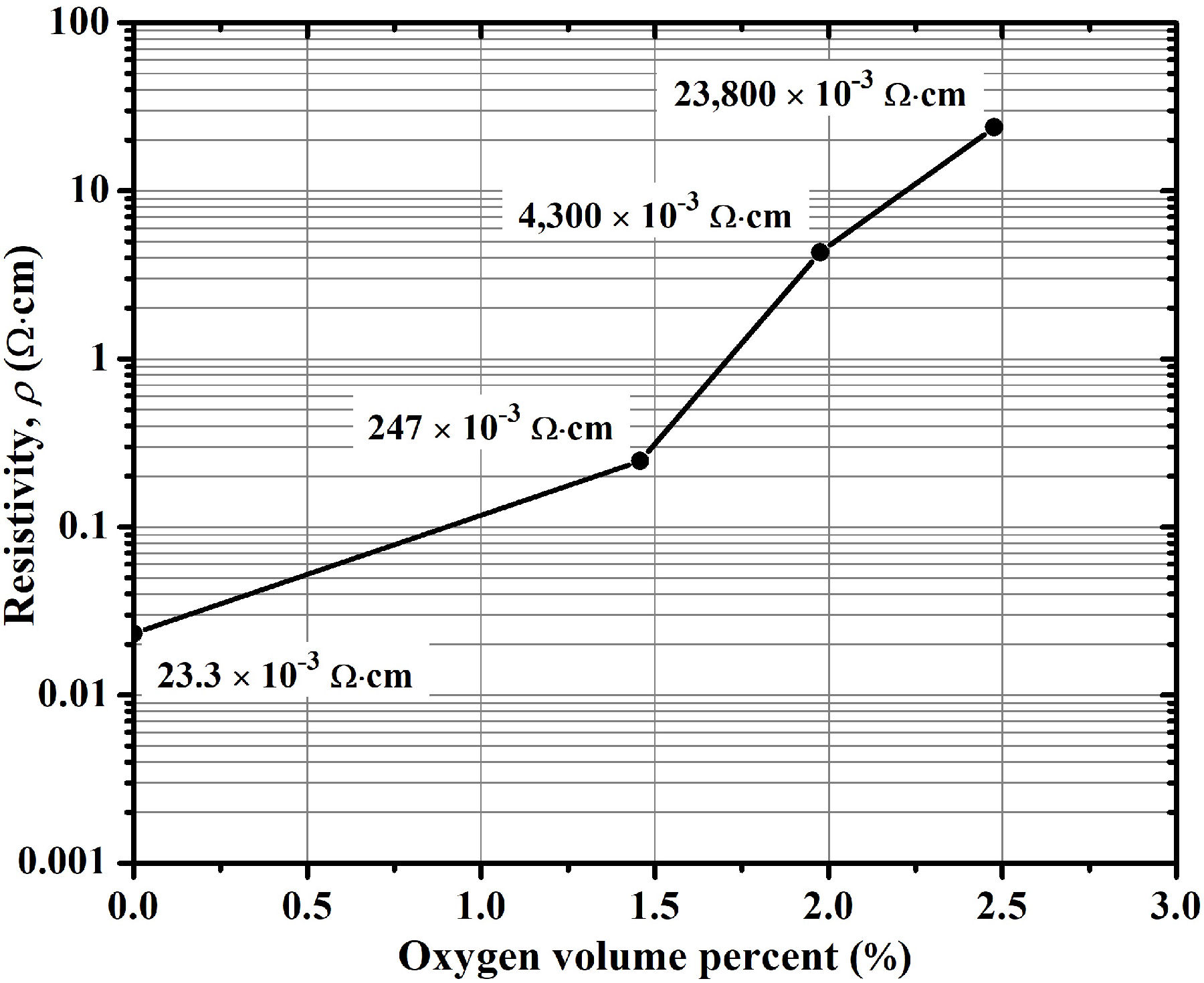
Figure 3 Variation of resistivity of the AZO thin films as a function of oxygen volume percent in the argon/oxygen mixture during the sputtering-deposition.  

Thus, as plotted in Fig. 4, we observed that the increase of the argon deposition pressure, without the addition of oxygen, increases the transmittance of the AZO thin films, and although an increase in the value of this deposition parameter also worsens the electrical properties, this occurs in a lesser extent compared to the use of oxygen during the film deposition. (For a better optical comparison, the transmittance spectra of these thin films are shown in Fig. 5). With this experiment, we also observed a clear and abrupt darkening of the AZO thin films when the argon working pressure is lower than 4.0 mTorr (0.53 Pa), although thin films deposited under this condition are more conductive (we indicate this argon pressure zone with a gray area in this and in the following figures). We partially conclude here that the use of higher argon pressure [higher than 4.0 mTorr (0.53 Pa)] under the deposition conditions previously described for this work (Sec. 2.1) is beneficial for the transmittance without greatly impacting on the electrical properties of the AZO thin film when good vacuum levels are achieved prior to the sputtering-deposition.

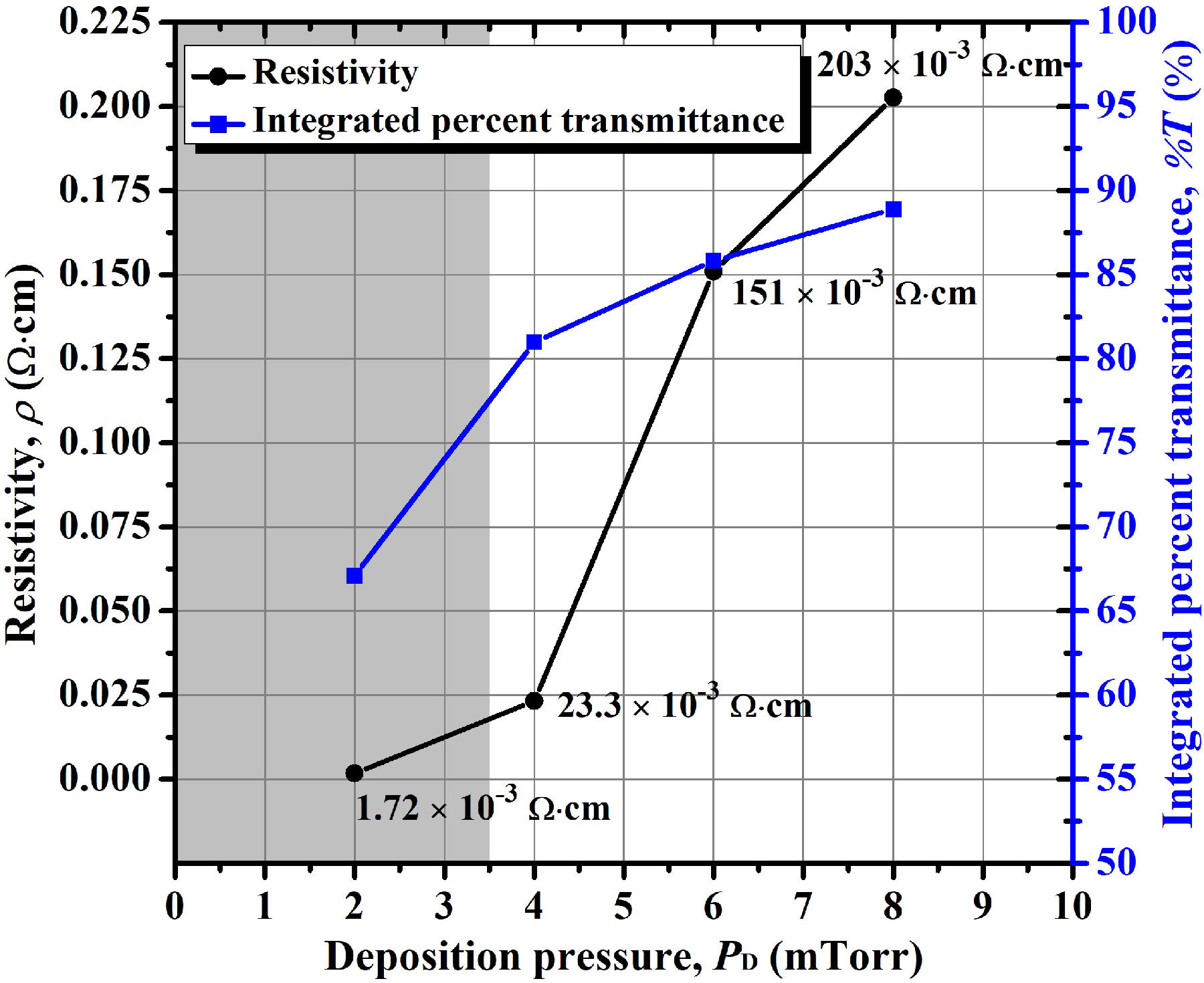
Figure 4 Variation of resistivity and integrated percent transmittance of the AZO thin films as a function of argon deposition pressure.  

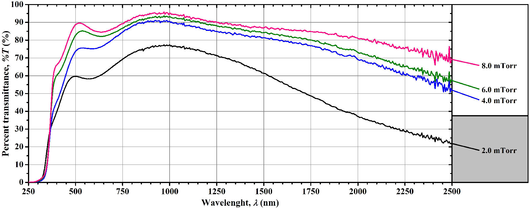
Figure 5 Percent transmittance spectra of the AZO thin films sputtering-deposited at different argon pressure values.  

Given that the vacuum level used in this work prior to the film deposition was constant and very low [good vacuum levels: 4.2×10⁻⁷ Torr (5.6×10⁻⁵ Pa)], the explanation of the results is less difficult than our previous work about the cases including the effect of residual gases [10]. Thus, the following text deals on the main parameters that we found to affect (more or less) the transmittance and resistivity of the AZO thin films.

To begin, Fig. 6 shows the XRD patterns of the AZO thin films deposited at different argon pressures. It is observed that all of the recorded diffractograms exhibit an intense peak at around 34.3°, which corresponds to the (002) crystalline plane of the ZnO hexagonal wurtzite structure, according to PDF # 36-1451. This indicates a c-axis preferred orientation perpendicular to the substrate surface. Furthermore, it can be observed other diffraction peaks showing lower intensity.

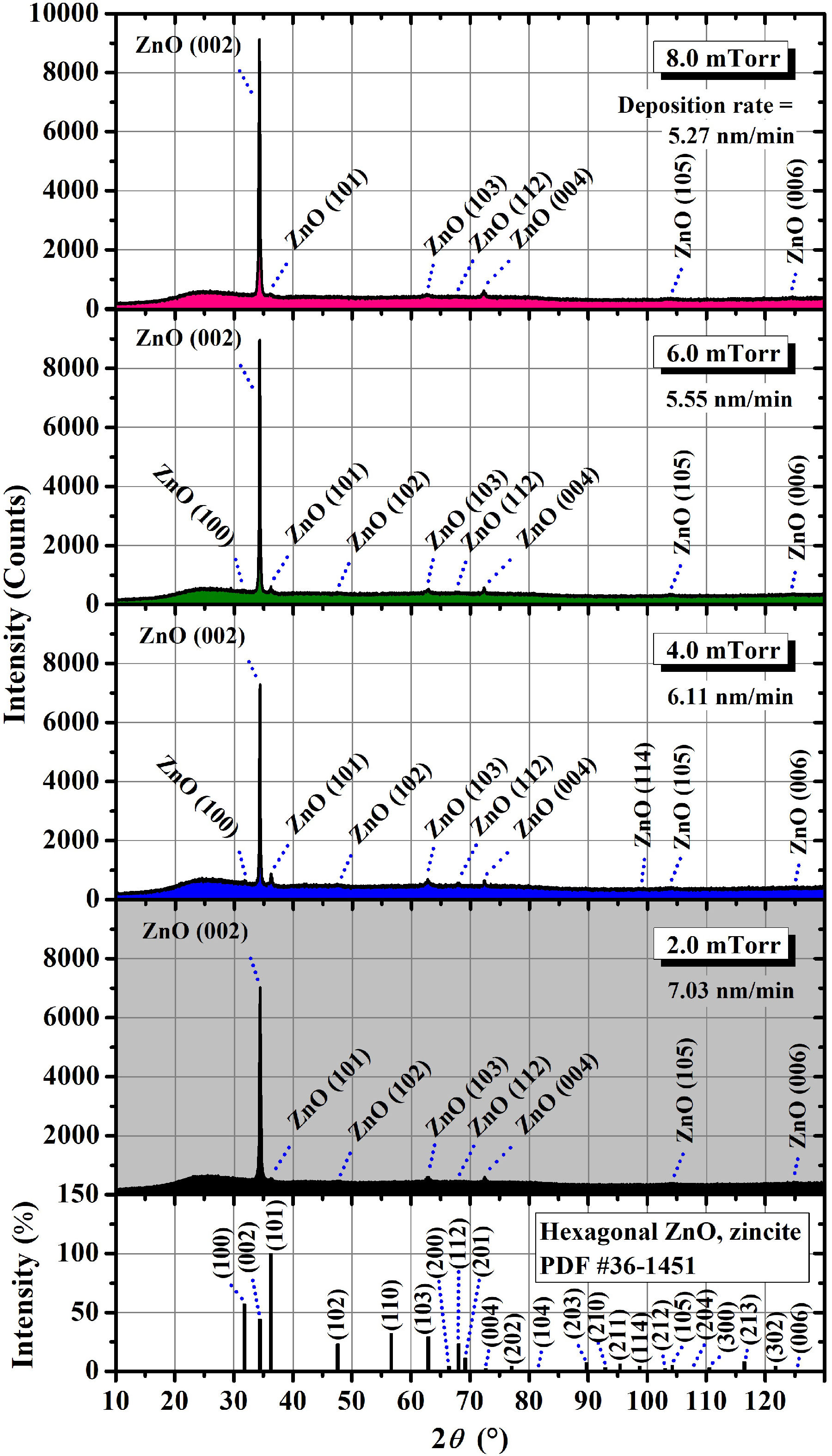
Figure 6 X-ray diffractograms of the AZO thin films sputtering-deposited at different argon pressure values.  

The most important of them are located at around 36.3, 62.8, 67.9, and 72.4​∘, which correspond, respectively, to the (101), (103), (112), and (004) crystalline planes of the same hexagonal structure. In a rough comparison, all the diffractograms present very similar characteristics. The difference, which will be discussed below, lies in the intensity of the XRD peaks, which can be taken as an approximate indication of the crystallinity of the films.

Figure 7 shows the change of deposition rate and the peak intensity of the (002) crystalline plane obtained from the XRD patterns of the AZO samples sputtering-deposited at different argon pressure values (Fig. 6). A clear diminution of deposition rate with the increase of argon deposition pressure is observed. Furthermore, the intensity of the peak corresponding to the (002) crystalline plane seems to inversely depend on the deposition rate at which the AZO thin films grow. This latter correlation was also observed in our previous work about the effect of the base pressure achieved prior to the sputtering-deposition [10], although in such a case the variation of the peak intensity was enormous due to the obtainment of deposition rates of even between 3 and 4 nm/min, a range that greatly affects the peak intensity of the (002) plane, this according to our previous paper [see Fig. 1(b)]. In such a paper, we reported that the deposition rate was strongly decreased by the presence of residual gases (that is, in bad vacuum levels), whose presence and subsequent dissociation probably exhaust the electron energy in the plasma, which results in a suppressed ionization of argon and, hence, in the decrease of deposition rate (as based on conclusions by Wang et al. [35] about the effect of water vapor on ITO films). For the present case, where the base pressure is constant, the phenomenon affecting deposition rate is distinct. Here, the increase of argon pressure increases the number of particles in the plasma discharge and thus increases the probability of collision, resulting in a reductionn ofn then mean free path and therefore in a diminution of deposition rate, thus increasing the peak intensity of the (002) crystalline plane.

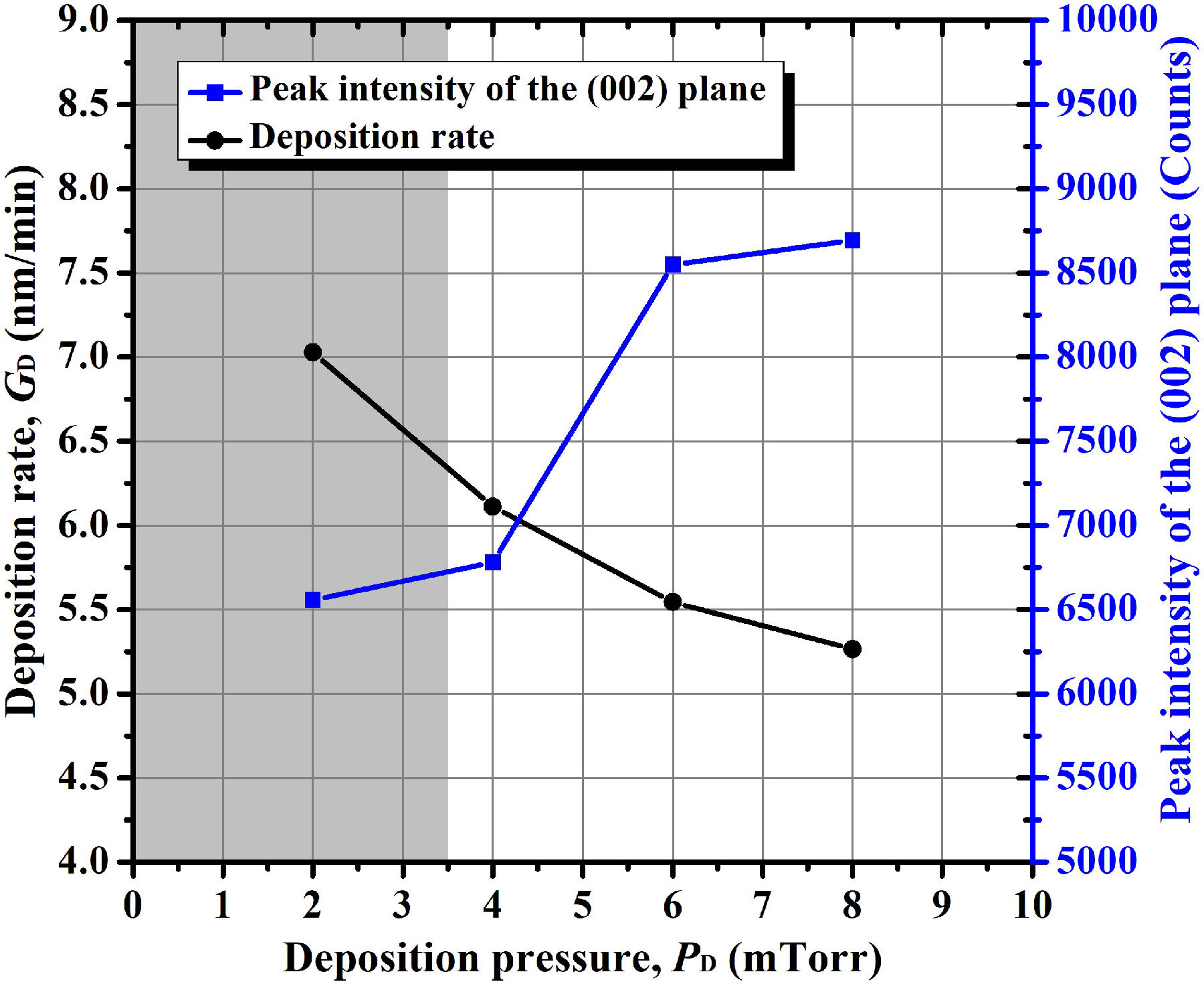
Figure 7 Variation of deposition rate and peak intensity of the (002) crystalline plane of the AZO thin films as a function of argon deposition pressure.  

It is important to note that the crystallinity showed by these AZO thin films deposited under different argon pressure values when a constant and very low base pressure is achieved [4.2×10⁻⁷ Torr (5.6×10⁻⁵ Pa)] is still very low compared to those AZO thin films deposited in our previous work at higher base pressure [10], that is, in the presence of residual gases. For example, for the case of deposition pressure equal to 4.0 mTorr (0.53 Pa), the AZO thin film deposited after achieving a base pressure of 4.2×10⁻⁷ Torr (5.6×10⁻⁵ Pa, which corresponds to the present work) shows a peak intensity of the (002) plane of almost nine times smaller than the thin film deposited after achieving 8.6×10⁻⁷ Torr (1.1×10⁻⁴ Pa) of base pressure. As mentioned in the previous paragraph, this difference in crystallinity is a consequence of the different deposition rates at which the AZO thin films grow. Furthermore, since in the previous work we observed that the films with low crystallinity also presented low transmittance, we tried to correlate both characteristics-note that the darkening was also observed in the present research, but at low argon deposition pressures, in a sample with slight lower crystallinity as compared with the others deposited at higher deposition pressures. However, our opinion was not that the darkening is a result of the low crystallinity of the films, but that the darkening is probably a result of a zinc excess in the film composition. In fact, the excess of zinc was correlated by Chou & Liu [36] with both the darkening and decrease of crystallinity of ZnO films. Although in our previous work the darkening of the AZO films coincided in almost all the cases presenting low-crystallinity (although, unfortunately, this correlation was not completely conclusive), it was difficult to find a good correlation with the excess of zinc (there was no obvious tendency between the base pressure and content of zinc, oxygen, and aluminum, which made clear the need for a careful chemical analysis of XPS data). Including, due to the complexity of the effect of base pressure, maybe other parameters also affected the transmittance of the films studied in our previous research. However, and fortunately, the correlation between the darkening and zinc excess (in terms of defects) results evident when they are studied at different deposition pressures with a constant base pressure, which constitutes a good finding of the present work. This correlation is thoroughly discussed below.

However, before discussing the chemical analysis, it is necessary to discard the parameters related with the structure of the AZO thin films as transmittance-determining factors. Thus, we also measured the crystallite size of the samples deposited by varying the argon pressure. For this, the Scherrer equation [Eq. (1)] was applied using the peak of the (002) plane. As a result, in Fig. 8 we plotted the variation of crystallite size with deposition pressure, in which it is observed that the variation of crystallite size is not very large (for the deposition pressure interval studied), and therefore it cannot be associated with the transmittance of the films. In fact, the magnitude of crystallite size seems not to be strongly related lated with other important parameters, like resistivity (as also shown shown in Fig. 8). Thus, as partial conclusions, when varying the argon pressure (in the interval studied), the obtained crystallite size does not largely define the optical and electrical properties.

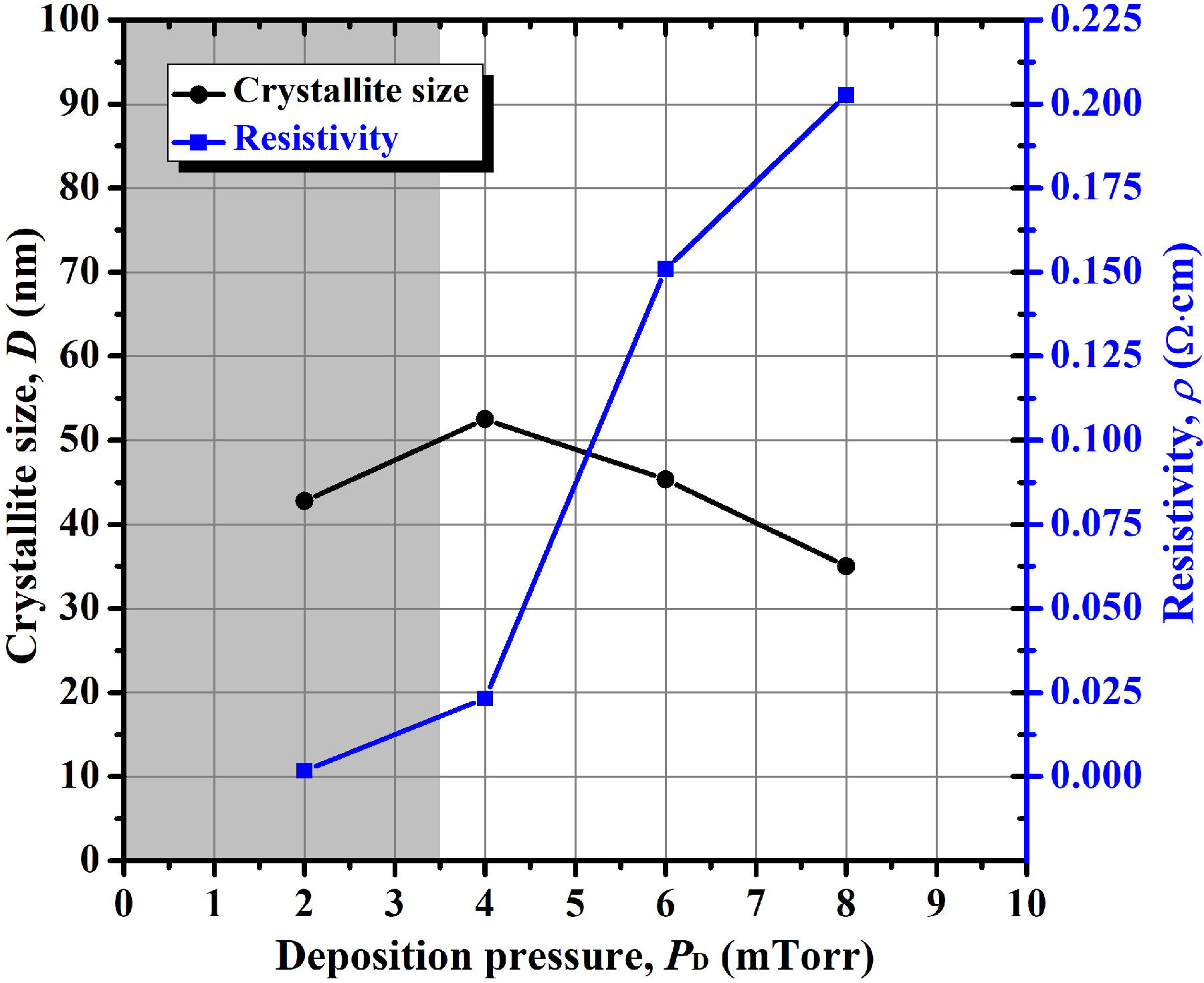
Figure 8 Variation of crystallite size and resistivity of the AZO thin films as a function of argon deposition pressure.  

At this point, it is now convenient to address the chemical analysis. To begin, the resolved high-resolution XPS spectra of the AZO thin films deposited at different argon pressures are shown in Fig. 9, and the positions for each determined component are presented in Table II. The Zn 2p3/2 spectra show a signal, the peak Zns, located at 1021.90 eV, which can be attributed to lattice zinc in crystalline ZnO [20,37,38]. Additionally, a signal labeled as peak Zni is found to appear consistently in all the spectra, with an energy position of 1022.98 eV, and which is possibly related to an interstitial defect and in direct connection to interstitial zinc [39]. On the other hand, the O 1s spectra show several photoemission lines corresponding to distinct oxygen chemical states. First of all, the peak Os, located at 530.38 eV, can be ascribed to lattice oxygen in the ZnO crystalline structure [38,40,41]. The peak OV, located at 531.28 eV, can be associated to oxygen in oxygen-deficient regions of the ZnO crystal, thus, it is maybe related to the presence of oxygen vacancies [38,41,42]. The peaks centered at 532.21 and 533.26 eV, labeled as OC1 and OC2, respectively, are related to adsorbed oxygen at the surface [38,39,41]; these types of oxygen are possibly bonded to carbon because, even after to the erosion treatment, it was found that their intensity increases alongside the carbon signal (C 1s not shown) with increasing deposition pressure (the erosion treatment was not enough to completely remove the adsorbed carbon, especially that from the samples obtained at high deposition pressures). Furthermore, the analysis interestingly shows a photoemission signal, labeled as peak Ox, centered at 529.23 eV, where its presence is probably related to an oxygen linked to aluminum. The rationalization for the latter considers a predominantly ionic bond and a simple theory for chemical shift, where the oxygen near to aluminum, or maybe even near to interstitial zinc, experience a different effective charge potential that leads to a lower binding energy when compared to the other oxygen chemical states. Finally, the Al 2p photoemission spectra show a single doublet peak centered at 74.15 eV (the Al 2p3/2, which for simplicity is not shown in Fig. 9, is located at 73.85 eV) with a spin-orbit splitting of 0.60 eV. The energy location of this aluminum can be related to aluminum occupying zincion sites in the crystalline lattice, which coincides with the positions identified by Chen et al. [38] and Das et al. [43] concerning substitutional aluminum in AZO films.

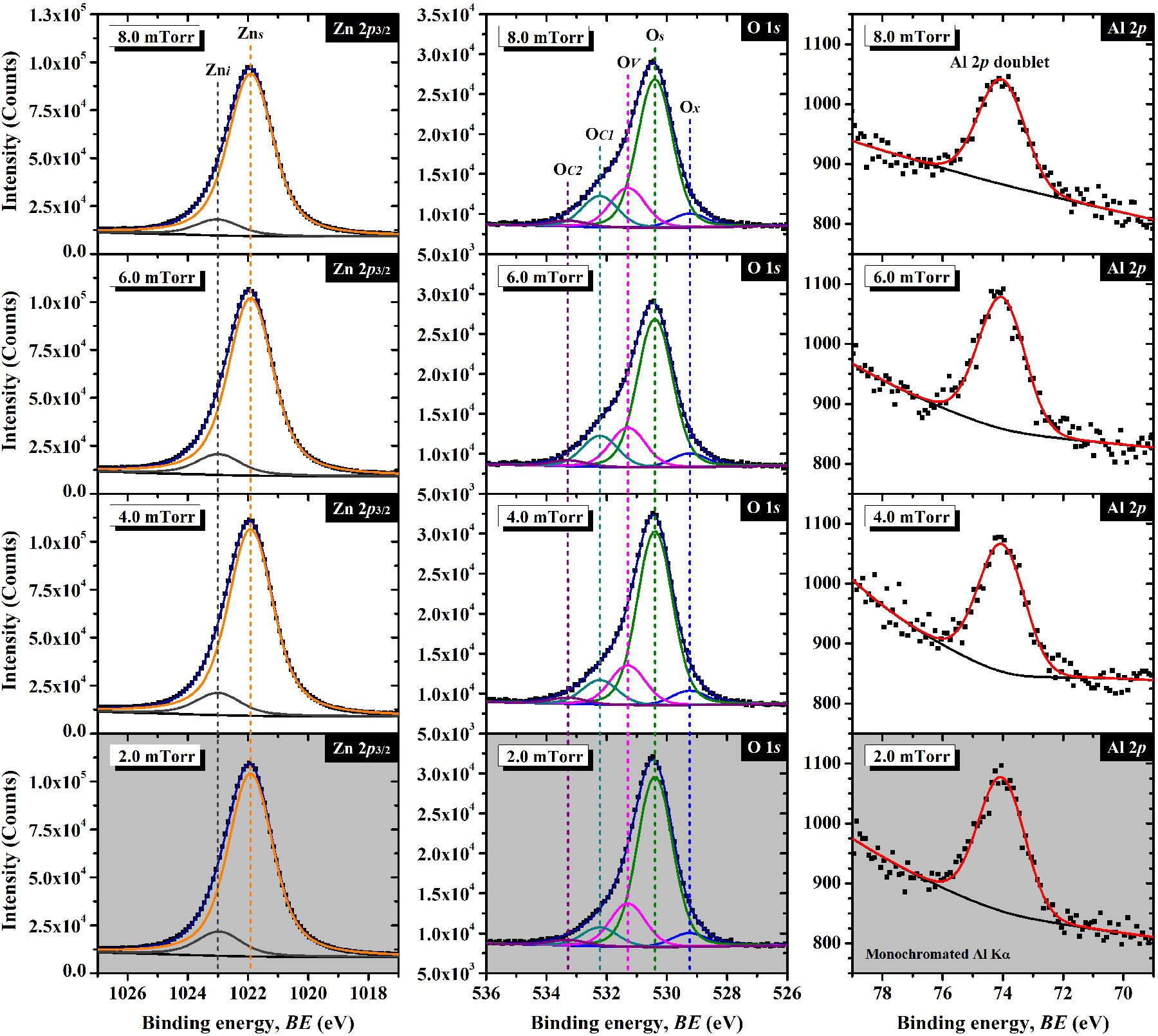
Figure 9 Resolved high-resolution photoemission spectra of the AZO thin films sputtering-deposited at different argon pressure values.  

As expected and mentioned in the previous paragraphs, the explanation for the variation of optical and electrical properties of AZO films deposited at different argon pressures was found after the chemical analysis of the samples. The results of this chemical analysis, as calculated from Eq. (2), are presented in Fig. 10. Here, we observed a dependence of the chemical composition, especially in terms of structural defects, with the change of argon pressure. For the discussion of data plotted in this figure, it is convenient to begin with the aluminum case, whose variation with deposition pressure does not seem to show a significant change, so its variation can be considered negligible, which simplifies the interpretation of the results. Therefore, the electrical and even the optical properties of the AZO material were affected mainly by the change of zinc and oxygen components as the deposition pressure is varied. Regarding to these components, it is also interesting to observe that the chemical composition assessment of peaks Zns and Os yields a Os/Zns ratio that is almost the same (between 1.05 and 1.02) independently of the deposition pressure employed. Note, however, that the peak Zns is lower in the film deposited at 2 mTorr (0.27 Pa), as compared with the rest of deposition pressures. This decrease is explained with the formation of zinc defects at low argon pressure. Similarly, the erratic change of the peak of Os can be explained with the presence of defect oxygen components affecting the lattice of ZnO. These types of defects are discussed below.

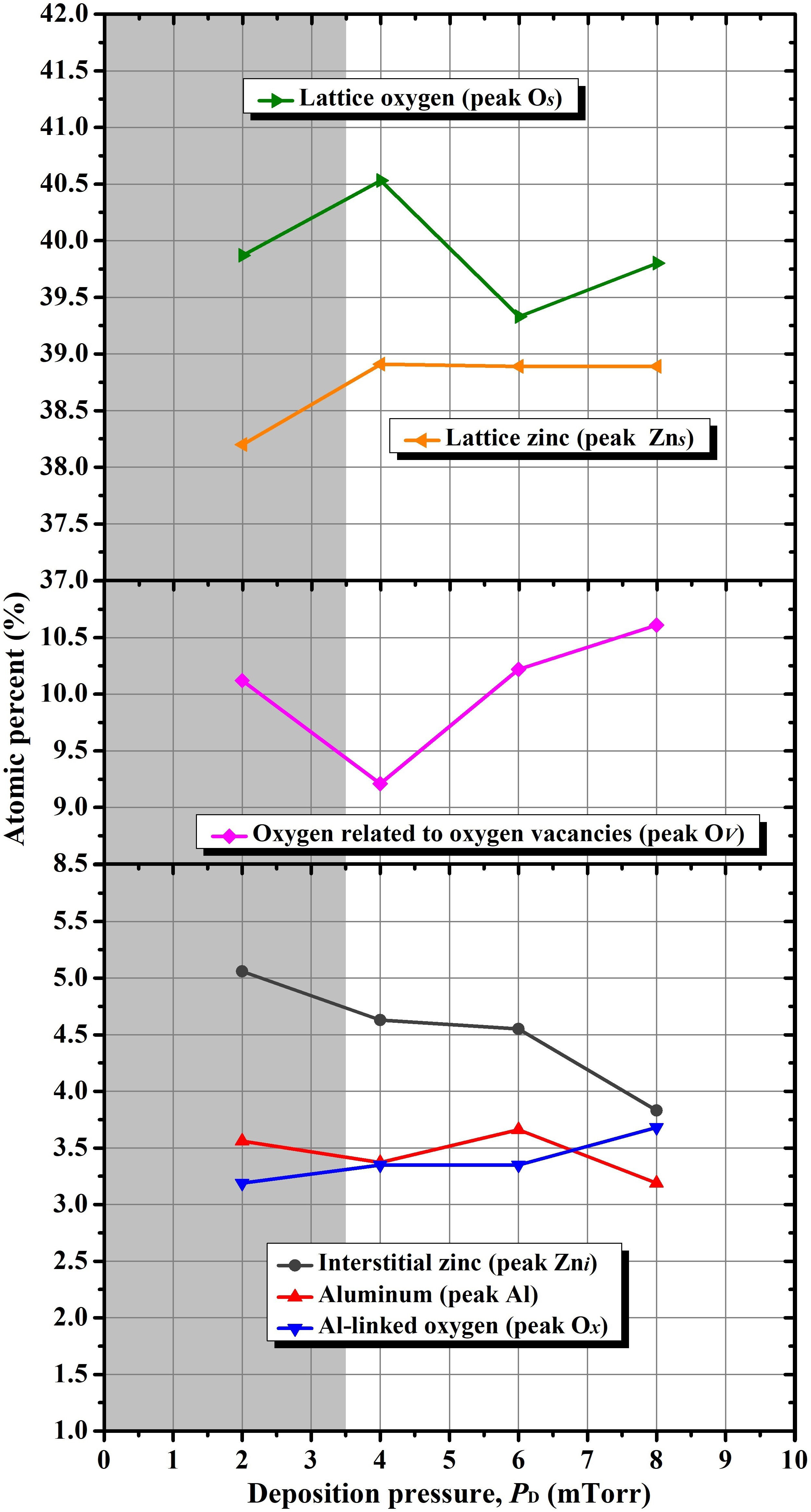
Figure 10 Variation of the chemical composition of the AZO thin films as a function of argon deposition pressure.  

A notable observation in Fig. 10 is the variation of the interstitial zinc content with increasing deposition pressure; the interstitial zinc content (represented by the peak Zni) is found to decrease at higher deposition pressures, and this, in turn, results in a more transparent film with a higher resistivity. This means that the interstitial zinc content may have a direct effect on the optical and electrical properties of the AZO thin films. The crystallinity slightly increases with the decrease of interstitial zinc, which suggests a possible correlation between them. The oxygen associated to oxygen vacancies (represented by the peak OV) also shows an interesting behavior; it shows an inverse tendency that has strong similitudes to the variation of the crystallite size as a function of argon deposition pressure. It is possible to observe that when the crystallite size is the largest, at a deposition pressure equal to 4.0 mTorr (0.53 Pa), the amount of oxygen vacancies is the lowest, which then increase with increasing deposition pressure and decreasing crystallite size. Another important aspect observed, is that when the AZO films are dark, it presents a large atomic percent of oxygen vacancies, which suddenly decreases when the AZO films turn transparent. Consequently, it is possible that the formation of more oxygen-deficient regions within the ZnO matrix, alongside with the increase of interstitial zinc, may result in an abrupt darkening of the AZO thin films. Possibly the nature of defects and their content in the AZO thin films can induce defects-related transitions (intragap states, similarly to the commonly accepted effect of the excess zinc) that enhance the electrical properties and a darkening of the films due to absorption in the visible region.

With this study, we found that the variation of deposition pressure, with only argon as working gas, affects the optical and electrical properties of the AZO thin films deposited in low content of residual gases. The use of deposition pressure equal and higher than 4.0 mTorr (0.53 Pa) under the conditions described in Sec. 2.1 leads to transparent and moderately conductive AZO thin films. Furthermore, the impact on the electrical properties is lesser when increasing the argon pressure than when introducing oxygen in the sputtering chamber. Also, an interesting explanation of the results was done based on the chemical composition analysis.

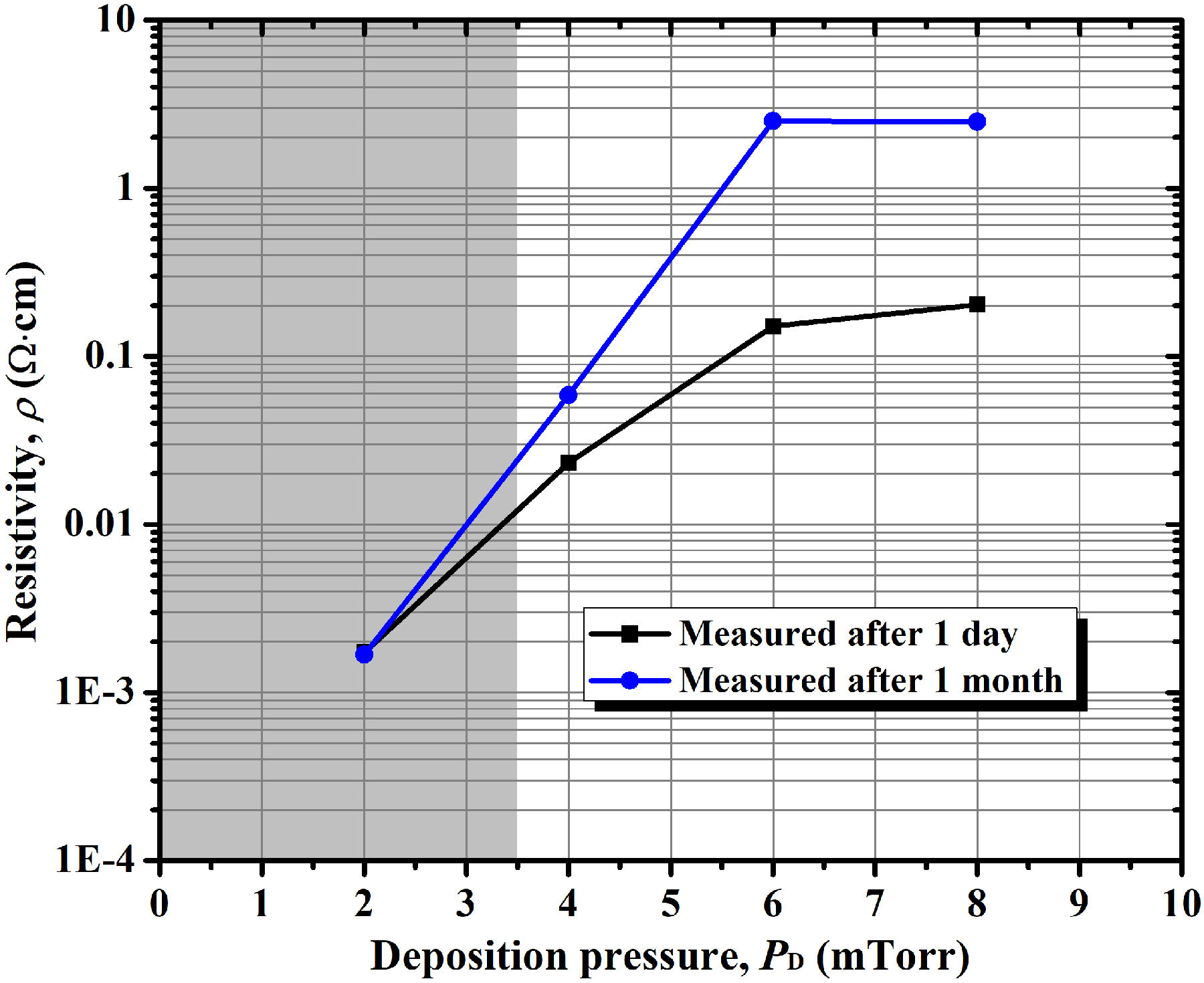
Finally, we want to include in this paper an additional preliminary experiment performed on the discussed AZO thin films with the aim of finding a rough indication of their stability to the environment. For this, we measured the resistivity of the AZO thin films again after one month of aging in the ambient air (under uncontrolled humidity and light). The resistivity of the films measured one day and one month after their deposition are plotted in Fig. 11. We observed here that thin films deposited at higher argon pressure do not only show higher resistivity, but also show more instability to the environment. Among the deposited films, the dark gray AZO thin film deposited at 2.0 mTorr (0.27 Pa) shows no change in resistivity, which indicates a high stability to the environment. The instability to the environment of the films deposited at high deposition pressures may be related to the neutralization of oxygen vacancies by oxygen provided by the environment during the days. In contrast, the film deposited at low deposition pressure (the dark zone) shows excellent stability probably due to the relatively high content of zinc interstitials that strain the lattice restricting the incorporation of ambient oxygen.

Figure 11 Change of resistivity of the AZO thin films measured one day and one month after the sputtering-deposition, expressed as a function of argon deposition pressure.  

4. Conclusions

We deposited by DC magnetron sputtering 260±20 nm AZO thin films after achieving a low base pressure of 4.2×10⁻⁷ Torr (5.6×10⁻⁵ Pa), which show a moderate integrated %T of 81.0% and a resistivity equal to 23 mΩcm when they are obtained at a deposition pressure of 4.0 mTorr (0.53 Pa) with only argon gas. Although it is known that the addition of oxygen gas during the sputtering deposition of AZO thin films is beneficial to the transmittance, we observed that the electrical properties are enormously affected. For example, an increase in resistivity from 23 to 247 mΩ∙cm was observed when the oxygen volume percent is increased from 0% to 1.5%. A high resistivity of about 24×103 mΩcm was obtained with an oxygen volume percent of 2.5%.

On the other hand, the increase in argon total pressure, without the addition of oxygen, also increased both the transmittance and resistivity, although the increase of the latter occurred in a lesser extent compared to the addition of oxygen. For example, an integrated %T of 88.9% and a resistivity of 203 m Ω∙cm were obtained by increasing the deposition pressure up to 8.0 mTorr (1.07 Pa). On the contrary case, the AZO thin film resulted in a dark gray color (%T equal to 67.1%) but good-conductive (1.7 mΩ∙cm of resistivity) when it is deposited at 2.0 mTorr (0.27 Pa).

The change of resistivity and transmittance was associated with the chemical composition of the AZO material: the lower the deposition pressure, the higher the interstitial zinc content in the AZO thin film. The increase in the content of interstitial zinc, alongside with oxygen vacancies, conferred to the films good electrical properties but poor transmittance. On the other hand, the aluminum content was almost constant (3.4%) along the studied deposition pressures.

Furthermore, we observed that the increase in deposition pressure decreased the deposition rate at which the AZO thin films grow. Also, with the decrease of deposition rate the peak intensity of the (002) crystalline plane was slightly increased (as compared with the effect of the base pressure). However, in the present study, we did not find a strong direct influence of these parameters on the optical and electrical properties, although the increase of the interstitial zinc content at low deposition pressure is probably related with the observed slightly decrease of crystallinity.

Acknowledgments

The Centres Científics i Tecnolo`gics de la Universitat de Barcelona (CCiTUB) are acknowledged for the assistance in XRD and XPS measurements. This research has been supported by the Spanish Ministerio de Economía, Industria y Competitividad (MINECO) and the European Regional Development Fund (ERDF) through the project CHENOC (ENE2016-78933-C4-2-R), and by the Mexican Consejo Nacional de Ciencia y Tecnología (CONACyT) through the projects with Registration Numbers 208159 and 251082. Jorge Alberto García-Valenzuela gratefully acknowledges the financial support from CONACyT.

References

1 I.L. Eisgruber, J.R. Engel, R.E. Hollingsworth, P.K. Bhat, and R. Wendt, J. Vac. Sci. Technol., A 17 (1999) 190. [ Links ]

2 M.-J. Jeng et al., Adv. Mater. Res. 213 (2011) 161. [ Links ]

3 P. Lv et al., Sci. China: Phys., Mech. Astron. 56 (2013) 1689. [ Links ]

4 G.S. Frankel, X.-B. Chen, R.K. Gupta, S. Kandasamy, and N. Birbilis, J. Electrochem. Soc. 161 (2014) C195. [ Links ]

5 B.H. Lee, C.-H. Yi, I.G. Kim, and S.-H. Lee, MRS Proc. 424 (1997) 335, edited by F. Funada, M. K. Hatalis, J. Kanicki, and C. J. Summers, presented at: 1996 MRS Spring Meeting, San Francisco, California, USA, April 4-12, 1996; [ Links ]

B.H. Lee , I.G. Kim , S.W. Cho, andS.-H. Lee , Thin Solid Films 302 (1997) 25. [ Links ]

6 M.G. Zebaze-Kana, E. Centurioni, D. Iencinella, and C. Summonte, Thin Solid Films 500 (2006) 203. [ Links ]

7 D.-K. Kim and H.-B. Kim, J. Alloys Compd. 522 (2012) 69. [ Links ]

8 N. Itagaki et al., presented at: 13th International Conference on Plasma Surface Engineering (PSE 2012), Garmisch-Partenkirchen, Germany, September 10-14, (2012) pp. 84-87. [ Links ]

9 H.-Y. Huo, M. Zou, G.-Q. Ma, and H. Chang, Surf. Technol. 42 (2013) 75. (in Chinese). Available at http://en.cnki.com.cn/Article_en/CJFDTotal-BMJS201301021.htm. [ Links ]

10 J.A. García-Valenzuela, J. Andreu, and J. Bertomeu, J. Vac. Sci. Technol. A 35 (2017) 021603. [ Links ]

11 R.G. Gordon, MRS Bull. 25 (2000) 52. [ Links ]

12 P. Scherrer, Nachr. K. Ges. Wiss. Göttingen, Math.-Phys. Kl. 1918 (1918) 98. Available at https://eudml.org/doc/59018. [ Links ]

13 B.E. Warren, X-Ray Diffraction [Dover Publications, Inc., Mineola, NY, USA, 1990 (Republication of the wok originally published by Addison-Wesley Pub. Co., 1969)] p. 253. [ Links ]

14 R. Saravanan and M. Prema Rani, Metal and Alloy Bonding: An Experimental Analysis-Charge Density in Metals and Alloys (Springer-Verlag London Limited, London, England, UK, 2012) p. 26. [ Links ]

15 J.F. Moulder, W.F. Stickle, P.E. Sobol, and K.D. Bomben, Handbook of X-ray Photoelectron Spectroscopy-A Reference Book of Standard Spectra for Identification and Interpretation of XPS Data, edited by J. Chastain and R. C. King Jr. (Physical Electronics, Inc., Eden Prairie, Minnesota, USA, 1995), pp. 64, 65. [ Links ]

16 J.A. García-Valenzuela et al., Thin Solid Films 619 (2016) 288. [ Links ]

17 A. Herrera-Gomez, analyzer®, a software for XPS-data peak-fitting, (2015). http://rdataa.com/aanalyzer/aanaHome.htmLinks ]

18 A. Herrera-Gomez , M. Bravo-Sanchez, O. Ceballos-Sanchez, and M.O. Vazquez-Lepe, Surf. Interface Anal. 46 (2014) 897. [ Links ]

19 A. Herrera-Gomez , M. Bravo-Sanchez , F.S. Aguirre-Tostado, andM.O. Vazquez-Lepe , J. Electron Spectrosc. Relat. Phenom. 189 (2013) 76. [ Links ]

20 D. Cabrera-German, G. Molar-Velázquez, G. Gómez-Sosa, W. de la Cruz, and A. Herrera-Gómez, Surf. Interface Anal. 49 (2017) 1078. [ Links ]

21 J.L. Campbell and T. Papp, At. Data Nucl. Data Tables 77 (2001) 1. [ Links ]

22 J.H. Scofield, J. Electron Spectrosc. Relat. Phenom. 8 (1976) 129. [ Links ]

23 A. Herrera-Gómez , A rigorous approach to the calculation of the uncertainties in XPS analysis, Internal Report, Centro de Investigación y de Estudios Avanzados del IPN (CINVESTAV), Unidad Querétaro, 2014. Available at http://www.qro.cinvestav.mx/ aherrera/reportesInternos/uncertaintiesXPS.pdfLinks ]

24 J. Muñoz-Flores andA. Herrera-Gomez , J. Electron Spectrosc. Relat. Phenom. 184 (2012) 533. [ Links ]

25 J.T. Grant, Surf. Interface Anal. 14 (1989) 271. [ Links ]

26 A. Herrera-Gomez , Self consistent ARXPS analysis for multilayer conformal films with abrupt interfaces, Internal Report, Centro de Investigación y de Estudios Avanzados del IPN (CINVESTAV), Unidad Querétaro, 2008. Available at http://www.qro.cinvestav.mx/∼aherrera/reportesInternos/arxpsAnalysisSharpIntefaces.pdf. [ Links ]

27 A. Herrera-Gomez et al., J. Electron Spectrosc. Relat. Phenom. 184 (2011) 487. [ Links ]

28 M. Bravo-Sanchez , J.A. Huerta-Ruelas, D. Cabrera-German , andA. Herrera-Gomez , Surf. Interface Anal. 49 (2017) 253. [ Links ]

29 A. Herrera-Gomez , J. Electron Spectrosc. Relat. Phenom. 182 (2010) 81. [ Links ]

30 J.J. Yeh and I. Lindau, At. Data Nucl. Data Tables 32 (1985) 1. [ Links ]

31 S. Tanuma, C.J. Powell, and D.R. Penn, Surf. Interface Anal. 21 (1994) 165. [ Links ]

32 C.J. Powell and A. Jablonski, NIST Electron Effective-Attenuation-Length Database - Version 1.3, National Institute of Standards and Technology (NIST), Gaithersburg, Maryland, USA, 2011. [ Links ]

33 H. Zhu, J. Hüpkes, E. Bunte, and S. M. Huang, Appl. Surf. Sci. 256 (2010) 4601. [ Links ]

34 N.-F. Shih, C.-C. Lin, and C.-Y. Kung, Jpn. J. Appl. Phys. 52 (2013) 01AC07. [ Links ]

35 M.H. Wang et al., Thin Solid Films 516 (2008) 5809. [ Links ]

36 K.-S. Chou and G.-K. Liu, Mater. Chem. Phys. 37 (1994) 156. [ Links ]

37 M.C. Biesinger, L.W.M. Lau, A.R. Gerson, and R.St.C. Smart, Appl. Surf. Sci. 257 (2010) 887. [ Links ]

38 M. Chen, X. Wang, Y.H. Yu, Z.L. Pei, X.D. Bai, C. Sun, R.F. Huang, and L.S. Wen, Appl. Surf. Sci. 158 (2000) 134. [ Links ]

39 F. Kayaci, S. Vempati, I. Donmez, N. Biyikli, and T. Uyar, Nanoscale 6 (2014) 10224. [ Links ]

40 K.E. Lee, M. Wang, E.J. Kim, and S.H. Hahn, Curr. Appl. Phys. 9 (2009) 683. [ Links ]

41 P.-T. Hsieh, Y.-C. Chen, K.-S. Kao, and C.-M. Wang , Appl. Phys. A 90 (2008) 317. [ Links ]

42 Q. Zhu, X. Bao, J. Yu, D. Zhu, Q. Zhang, C. Gu, H. Dong, R. Yang, and L. Dong, Thin Solid Films 605 (2016) 202. [ Links ]

43 A.K. Das, P. Misra, R.S. Ajimsha, A. Bose, S.C. Joshi, D.M. Phase, and L.M. Kukreja, J. Appl. Phys. 112 (2012) 103706. [ Links ]

Received: June 25, 2018; Accepted: July 02, 2018

Creative Commons License This is an open-access article distributed under the terms of the Creative Commons Attribution License