


 nueva página del texto (beta)
 Inglés (pdf)
 Artículo en XML
 Referencias del artículo
 Enviar artículo por email
 Citado por SciELO
  Similares en
SciELO
Similares en
SciELO 
 Permalink
PACS: 42.55.Px; 42.79.Ry; 42.60.Jf; 47.27.ek
1. Introduction
Group-III nitride laser diodes (LDs) commercially available since 2000 are nowadays used in a wide range of applications such as: optical data storage, printing and photolithography1,2, but in spite of their great success, these devices still suffer from various problems and are far from being optimized. One of the unsolved problems is the leakage of optical field to the substrate by the insufficient optical confinement. This is due to the difficulty to growth the thick AlGaN cladding layers with high aluminum content needed to ensure an efficient waveguide3-5. The leakage of the optical field affects the beam shape which is critical in applications such as data storage and laser projection.
On the other hand the presence of GaN contact layers with larger refractive index compared to AlGaN cladding layers causes an anti-guide effect in the optical cavity of the structure6. As a result, high order modes in the waveguide occur, affecting both the near and far field patterns7.
Another problem in fabrication of nitrides based LDs is the lack of native GaN substrates. Presently InGaN based LDs are grown onto sapphire or SiC substrates8. This results in high threading dislocation densities in the structure because of thermal and lattice mismatch9,10.
Recently GaN substrates have been used to growth LD structures11,12 but this aggravates the problem of the optical field leakage to substrate as illustrated in the experimental works of T. Swietlik et al.13 and J. Dorsaz et al.12. In this case the anti-guide effect is more pronounced since the GaN substrate layer is added to the n-GaN contact layer resulting in a much thicker layer of higher refractive index than the cladding layer.
Studies of InGaN LDs grown onto sapphire substrates shown that the detrimental effects produced by the anti-guide problem on the, confinement factor, near-field patterns (NFPs) and far field patterns (FFPs) can be minimized by properly choosing the thickness and composition of the different layers forming the heterostructures14-16.
To fabricate efficient waveguides with not optical leakage, very thick claddings layers are usually gown in arsenide-based lasers. Unfortunately, in case of nitride material system, there is a significant lattice mismatch between AlN and GaN8, which strongly limits the thickness attainable in the AlGaN cladding layers. AlGaN layers thicker than the critical thickness tend to crack and the stress introduced in the Alx Ga1−x N cladding layers results in poor quality material7,17.
Owing to the limitation in the thickness of the AlGaN layer can be growth; different approaches have been proposed to reduce the leakage of the optical modes to the substrate. Recently Muziol et al proposed a design in which the leakage has been fully suppressed by using a high-indium-content thick InGaN waveguide18.
In this work we analyze the influence of GaN substrate thickness on the optical confinement
factor, near and far field patterns in InGaN lasers. Simulation was done replacing
the n-GaN contact layer by an n- Alx
Ga1−x
N grading layer
2. Laser diode structure and parameters used in simulation
A schematic of the laser structure used in simulations is shown in Fig. 1. It is a separate confinement optical cavity (SCH) similar to that reported in 19 but with a GaN substrate. The active regions consist of a two 3 nm-thick In0.15Ga0.85N wells sandwiched between two 6 nm-thick In0.05Ga0.95N barriers. A 20 nm p-Al0.2Ga0.8N electron blocking layer (EBL) is placed above the outermost barrier. The waveguide is comprised by two 0.1 µm-thick-GaN layers surrounded by the 0.7 µm-Al0.15Ga0.85N cladding layers. The structure is completed with a 2 µm- n-GaN, and 1.0 µm-p-GaN contact layers. In the study we analyzed the effect of replace the n-GaN contact layer by a 2 µm-n- Al
x
Ga
1−x
N GRIN contact layer with a parabolic variation of the Al composition
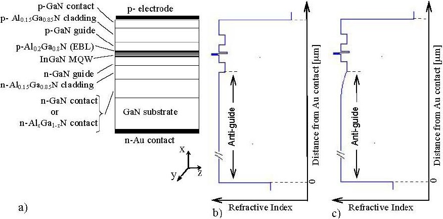
Figure 1 a) Schematic of the laser structure used in simulation, b) Refractive index profile for the straight structure and c) for structure with a GRIN n- Alx Ga1−x N contact layer.
Table I Layer structure and physical parameters used in simulation.
| refractive index | thickness | ||
| n | k | ||
| p-contact | 0.9 | 2.5 | |
| p-GaN contact | 2.537 | 0 | 1.0 µm |
| p-Al0.15Ga0.85N cladding | 2.456 | 0 | 0.7 µm |
| p-GaN guide | 2.537 | 0 | 0.1 µm |
| p-Al0.2Ga0.8N (EBL) | 2.434 | 0 | 20 nm |
| 2 QW’s active | |||
| In0.15 Ga0.85 N well | 2.625 | 0 | 3 nm |
| In0.05 Ga0.95 N barrier | 2.553 | 0 | 6 nm |
| n-GaN guide | 2.537 | 0 | 0.1 µm |
| n-Al0.15Ga0.85N cladding | 2.456 | 0 | 0.7 µm |
| n-GaN contact | 2.537 | 0 | 2.0 µm |
| GaN substrate | 2.537 | 0 | 1 -100 µm |
| n-Au contact | 1.561 | 1.82820 | |
As can be seen in Fig. 1 and Table I, the refractive index of the p-GaN and n-GaN contact layers is larger than that of the AlGaN Cladding layers and guided modes can leakage from waveguide. As previously said, this leakage can be avoided by growing thick AlGaN cladding layers, but unfortunately, it is difficult to grow a good quality thick AlGaN layer.
3. Calculation
The scalar wave equation of the fields was used to calculate the confined modes in the waveguide:
Here,
The Runge-Kutta-Nystrom method was used to obtain the numerical solution in the GRIN-layer since Eq. 1 has not an exact solution in this layer. In the rest of the layers the exact solutions of the wave equation were obtained as was done in Ref. 21.
From the relation between the magnetic component
Hz
and the electric field component
Ey
, we get the appropriate boundary conditions at the different interfaces to obtain a complete solution of the problem22. The dispersion law was obtained by using the transfer matrix method. The solution of the dispersion equation was found using the method of testing for transcendental equations. From these solutions the effective refractive index of the fundamental mode No was obtained. The near field
The confinement factor
Notice that in a MQW structure the confinement factor is given by the summation of the value of the confinement factor for each QW. The confinement factor tells about the extent to which an optical mode is confined to the active region so is desirable to have the greatest possible value of this parameter for a good laser performance.
The far-field pattern perpendicular to the junction plane of the laser structure is the product of the Fourier transform of the near field
4. Results and Discussion
The effect of the GaN substrate thickness on the confinement factor, near and far field patterns in nitride laser was numerically simulated. The values of the refractive index used for calculation are taken at the wavelength of 410 nm, the emission wavelength reported for our experimental reference device.
Figures 2 to 6 show the impact of substrate thickness on the confinement factor and near field patterns. In all cases Al0.15Ga0.85N claddings and n-GaN contact layer are set to 2 and 0.7 µm respectively. The insets show the resultant far field pattern and the full wide at half-maximum (FWHM) values in each case. The substrate thickness was changed from 1 to 100 µm. It is important to point out that currently available GaN substrates have a small thickness. There are no GaN ingots as those of silicon and GaAs, so costly, free-standing substrates are obtained by growing a GaN layer onto other substrates and then cut into wafers. Typically GaN substrates from 3 to 8 microns are obtained5
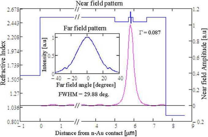
Figure 2 Calculated near and far field (inset) intensity patterns for 3 µm thick GaN substrate. Values of the confinement factor and FWHM are also shown. In this case the near field pattern is smooth indicating a good optical confinement and that there is almost not leakage of the optical field into the substrate.
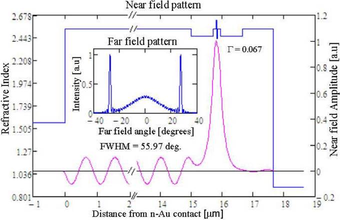
Figure 3 Calculated near and far field (inset) intensity patterns for 13 µm thick GaN substrate. Values of the confinement factor and FWHM are also shown. In this case the near field pattern has many ripples, resulting in pronounced peaks at both sides of the central maximum in the far-field pattern. This result indicates that for this value of the substrate thickness the optical leakage into substrate is remarkable.
Figure 4 Calculated near and far field (insert) intensity patterns for a 36 µm thick GaN substrate. In this case and contrary to what you would expect, results are very similar to those of the Fig. 2 indicating this substrate value provides an efficient optical waveguide.
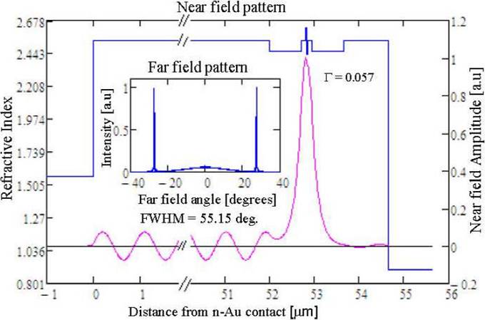
Figure 5 Calculated near and far field (insert) intensity patterns for a 50 µm thick GaN substrate. In this case a very low value of the confinement factor is obtained; again ripples in the near field patter appear indicating the leakage of optical modes to GaN substrate.
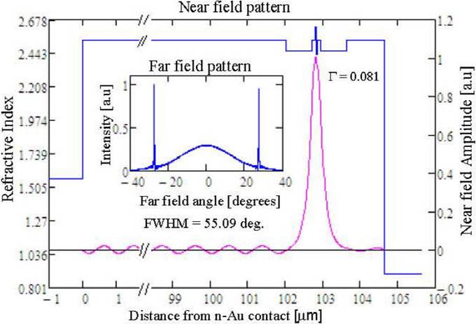
Figure 6 Calculated near and far field (insert) intensity patterns for a 100 µm thick GaN substrate. Here although the thickness of the substrate is double of that in previous figure, the confinement factor and the far and near field patterns improve and the optical leakage is reduced. This result proves the fluctuating behavior of theses parameters regarding the substrate thickness.
As can be seen from these figures and contrary to what might be expected, the near field pattern and the confinement factor do not worsen in a continuously way as the thickness of the substrate is increased. Instead a fluctuating behavior is observed and there are specific values for which highest values of the confinement factor and lowest values of the FWHM are obtained. For example for a substrate thickness of 13 µm the near field pattern has many ripples and two pronounced peaks at both sides of the central maximum can be observed in the resulting far-field pattern. However, for a substrate thickness of 36 µm the parasitic ripples on the NFP almost disappeared and the peaks on the far field pattern are significantly reduced.
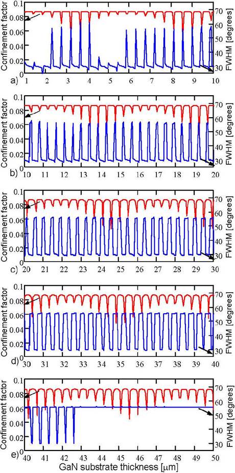
In Fig. 7, the confinement factor and FHWM values obtained for substrate thickness from 1 to 50 µm are shown. Here the oscillating behavior of the confinement factor and the FWHM can be noticed in more detail. These results show there are critical values of the substrate’s thickness for which
The number of critical points can be reduced by using thicker cladding layers as it is shown in Figs. 8 and 9. These figures show the dependence of
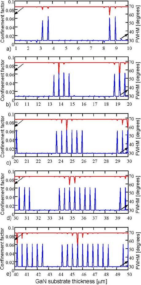
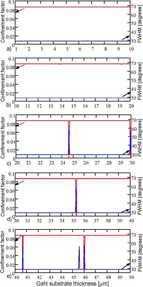
Figure 9 Calculated of Γ and FWHM as a function of substrate thickness for 1.5 µm Al0:15Ga0:85N cladding layers.
For a cladding layer thickness of 1.5 µm, no fluctuation in
Figure 10 shows that the same effect can be obtained by replacing the n-GaN contact layer with a GRIN Alx Ga1−x N layer. The NFP and FFP patterns obtained for a 2 µm-n-Alx Ga1−x N layer with a parabolic variation of Al composition from 0 to 0.15 are shown. Simulation was done for a substrate of 100 µm and a 0.7 µm Al0.15Ga0.85N cladding layer. No ripples in the NFP are observed and a Gaussian-shaped far-field pattern is obtained in this case.
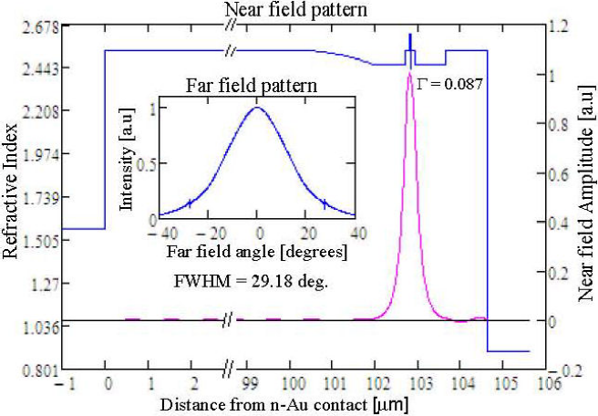
Figure 10 Calculated Near and Far field (inset) intensity patterns for a 100 µm GaN substrate, 0.7 µm Al0.15 Ga0.85 N cladding layers and 2 µm n-Alx Ga1-x N (0 ≤ x ≤ 0.15) GRIN contact layer. Values of the confinement factor and FWHM are also shown.
Figure 11 shows the dependence of
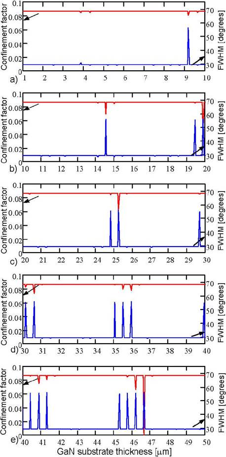
Figure 11 Dependence of Γ and FWHM on substrate thickness for 0.7 µm Al0.15 Ga0.85 N cladding layers and 2 µm n-Alx Ga1-x N (0 ≤ x ≤ 0.15) GRIN contact layer.
Finally the dependence of
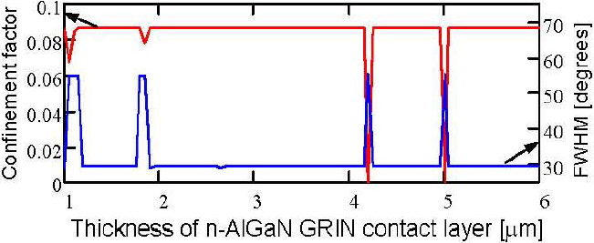
Figure 12 Dependence of Γ and FWHM on the n- Alx Ga1-x NGRIN layer thickness for a 100 µm GaN substrate and 0.7 µm Al 0.15 Ga 0.85 N cladding layers.
Simulation results reveal there are substrates thicknesses for which the optical field
accommodates better in the waveguide with a less penetration in the anti-guides,
resulting in a high value of the confinement factor, and a low value of the FWHM of
the far field pattern, as desired. Also observed is the existence of critical points
for which
5. Conclusions
In this paper, we have analyzed the effect of the GaN substrate thickness on the optical field in InGaN laser diodes. Near and far-field patterns perpendicular to the junction plane were calculated by solving the wave equation. Results revealed a fluctuating behavior, for some values of the substrate thickness the NFPs and FFPs can be optimized and the optical field leakage towards the substrate is substantially reduced. Also, there are critical values of the substrate thickness that produce the lowest values of the confinement factor and the higher values for the FWHM which should be avoided. These results indicating that the thickness of GaN substrate is a critical parameter in the design of the optical cavity in nitrides lasers. It is shown that appropriately choosing the thickness of the substrate and replacing the n-GaN contact layer by a GRIN- Alx Ga1−x N layer it is possible to improve both the confinement factor and Far field pattern in nitride lasers and the performance of the InGaN quantum-well lasers can be enhanced.

