


 text new page (beta)
 English (pdf)
 Article in xml format
 Article references
 Send this article by e-mail
 Cited by SciELO
  Similars in
SciELO
Similars in
SciELO 
 Permalink
PACS: 81.07.Bc; 81.16.Be; 61.05.cp; 61.46.Df; 61.72.uj; 78.30.Fs; 78.40.Fy; 78.55.Et
1. Introduction
Semiconductor nanostructures have attracted a lot of attention due to their unique mechanical, optical and electronic properties. Inorganic compounds doped with lanthanide ions are widely used as the luminescent materials in lighting1 and displays2, optical amplifiers3 and lasers4. Lately, the optical properties of crystal nanomaterials doped with lanthanide impurities have attracted much attention as they are expected to modify both electronic states and optical properties. Consequently, a possible influence of quantum size effect on the luminescence properties is expected for II-VI semiconductor compound nanocrystals due to the inclusion of rare earth (RE) metal ions5. The effects of the quantum confinement size of the semiconductor nanoparticles not only create photogenerated carriers, which may have an interaction with f-electrons but also significantly influence the optical properties6. Therefore, excitonic transition in the host material and an improvement in the luminescence intensity is also expected for the semiconductor nanostructures after the rare earths (RE) doping. The effects of the reduced dimensionality on the electronic relaxation and the phonon density-of-states of semiconductor compounds and insulating nanocrystals have been extensively investigated by both theoretical and experimental approaches7,8.
Doping of II-VI semiconductors compounds with rare earths ions like cerium, terbium and europium, etc., has recently been extensively studied9. Doping by rare earth elements such as cerium reduces the particle size of the nanomaterials and increases the effective surface area10. Vij et al. reported the optical property studies on Ce doped SrS nanostructures and Ce doped CaS nanoparticles synthesized by solid state diffusion method11. Kumar et al.12 have reported luminescence investigations on Ce3+ -doped CaS synthesized using the chemical co-precipitation method.
In this work reports the structural and optical characterization of CdS and CdS:(Ce3+, Eu3+) nanofilms obtained by chemical bath deposition on glass substrate synthesised at 70 ± 2°C at different synthesis times for varying the rare earth molar concentration. The effects of the chemical composition on structural and optical properties of the CdS and CdS:(Ce3+,Eu3+) were studied by EDS, X-ray diffraction, HRTEM, Raman spectroscopy, transmittance and photoluminescence at room temperature.
2. Experimental details
The growth technique to obtain the CdS doped with rare earth is the chemical bath
deposition13 in its modality
of immersion, in which a cryo-thermostat of circulation Polyscience with temperature
controller of -40 to 200°C was used. Being graded it at the temperature of 20°C to
avoid the release of harmful gases into the environment and using ammonium nitrate
as complexing agent. The solutions mixture is carried out using the following
precursors: cadmium chloride dehydrate (CdCl2+2H2O) (Productos
Químicos Monterrey S.A.), potassium hydroxide (KOH) (JT Baker, 98.6% purity),
Ammonia Nitrate (NH4(NO3)) (Sigma-Aldrich, 99.5% purity) and
thiourea thiocarbamide (Fermet, 99.9% purity). The nitrifying reagents are europium
(III) nitrate pentahydrate (Eu(NO3 )3+5H2O)
(Sigma-Aldrich, 99.999% purity) and cerium (III) nitrate
(Ce(NO3)3+6H2O) (Sigma-Aldrich, 99.999% purity)
working with the following concentrations 0.05 M CdCl2, 0.05 M KOH, 0.1 M
NH4(NO3), 0.05 M NH2 SCNH2. The
precursor concentrations are Eu(NO3)3 0.001 M and
Ce(NO3)3 0.001 M with the appropriate volumes, the doping
is achieved when the solutions mixture has a slightly basic pH. The increase in the
doping molar concentration is performed by increasing the synthesis time, which was
ranged from 60 to 135 min., achieving yellowish-opaque surfaces. The synthesised
samples are shown in Table I and the number
that accompanies the sample name corresponds to the synthesis time. The
CdS:(0,Eu3+,Ce3+) nanofilms chemical stoichiometry was
obtained by Energy Dispersive Spectrometry (EDS), which was carried out in a System
LEO 438VP, with W.D. of 26 mm using a pressure of 20 Pa. The crystalline phase and
structure of the nanocrystals were determined with a Bruker D8 Discover
diffractometer using the copper KÆ radiation
Table I It presents the CdS:RE3+ synthesised nanofilms and the doping volume added to each one. Additionally, the Cd, S and RE molar concentrations of the nanofilms that were estimated by EDS. The average errors with that were estimated percentage masses of different elements were for cadmium 1.25%, sulphur 0.35%, europium 0.25% and for cerium 0.30%.
| Sample | RE(NO3)3 Added volume (ml) |
Cd mass weight (%) |
Cd molar fraction (%) |
S mass fraction (%) |
S molar fraction (%) |
RE mass fraction (%) |
RE molar fraction (%) |
| M60 | - | 80.66 | 54.32 | 19.34 | 45.68 | - | - |
| M65 | - | 79.20 | 52.06 | 20.80 | 47.94 | - | - |
| M70 | - | 78.31 | 50.74 | 21.69 | 49.28 | - | - |
| M74 | - | 77.11 | 49.01 | 22.89 | 50.99 | - | - |
| Eu(NO3)3 | Eu | Eu | |||||
| M105 | 1 | 80.62 | 56.79 | 17.16 | 42.36 | 2.23 | 0.85 |
| M115 | 2 | 80.25 | 57.12 | 16.71 | 41.70 | 3.04 | 1.18 |
| M125 | 3 | 78.98 | 56.87 | 16.37 | 41.32 | 4.65 | 1.81 |
| M135 | 4 | 71.06 | 43.10 | 22.54 | 47.57 | 5.86 | 3.47 |
| Ce(NO3)3 | Ce | Ce | |||||
| M80 | 1 | 74.55 | 46.45 | 24.24 | 52.95 | 1.21 | 0.60 |
| M100 | 2 | 75.64 | 48.01 | 23.06 | 51.32 | 1.31 | 0.66 |
| M130 | 3 | 71.06 | 44.03 | 25.26 | 54.32 | 3.68 | 1.65 |
3. Experimental results and discussion
The chemical stoichiometry of the CdS:RE3+ nanofilms was estimated by EDS measurements. Figure 1 shows EDS spectra of two typical samples, M100 and M115. The information of the most elementary elemental composition (spot analysis) was generated by keeping the electron beam fixed at several points of the sample, in which the total scan was performed (global analysis), which besides allowed to know the presence of the residual impurities as oxygen in the samples along with cadmium and sulphur. It has been found that oxygen ions are present in the layers in the form of O2- ions, which could produce CdO14,15. These oxygen ions form trap levels in the band gap, resulting in several radiative or non-radiative transitions contributing or affecting to the luminescence, since that O2- ions replace sulphur atoms at some random points of the S sub-lattice. The EDS measurements are presented in Table I, in which are included the atomic and mass percentages of the elements. From these results is observed that CdS samples are not stoichiometric. As is known the atomic weight of the ideal unit cell is ~288.95 u that corresponds to 22.19% sulphur atoms and 77.81% cadmium atoms. Therefore, if there is excess cadmium and lack of sulphur that is indicative that cadmium is interstitial and there are vacancies of sulphur16. Table I shows that the nanofilms contain a lower concentration of sulphur, indicating that have a high concentration of sulphur vacancies. Also, it can induce that there is a high concentration of cadmium and RE interstices16.

Figure 1 EDS spectra of two CdS typical samples, which show clearly the presence of rare earths in the nanofilms: a) M100 and b) M115.
Figure 2 shows X-ray patterns of typical CdS:(Ce,Eu) nanofilms with different rare earths molar concentrations deposited at temperature of 70 ± 2°C, which were synthesised at different times. It is observed from XRD patterns that CdS:RE3+ deposited nanofilms are in polycrystalline nature. As can be seen, the diffraction pattern of the M65 sample shows clearly a predominant peak at 2θ = 26.76°, which can be assigned to (111) plane of ZB CdS crystalline phase, indicating a preferential growth orientation. In addition, it can be seen that each peak corresponds fairly well with data of CdS marked in the software DICVOL04 data. The lattice constant obtained with the software DICVOL04 data is in good agreement with the published results 16, obtained values of the lattice parameter that are shown in Table II and Fig. 3 that confirmed that the CdS:RE3+ nanofilms for all the molar concentrations belong to face-centered cubic system and their X-ray patterns are described in the F m - 3m(225). For rare earth doped films diffractograms, the appearing of new diffraction peaks are associated to the incorporation of RE3+ at the sub-lattices sites of Cd2+ . As is clearly seen in Fig. 3 the CdS:Ce3+ diffractograms present two dominant diffraction peaks at 17.26 and 26.76°, first one is associated to (102) diffraction plane of Ce2S3 and the second is assigned to (111) plane of ZB CdS crystalline phase. Besides, two small diffraction peaks at 28.44 and 34.73° that are associated with Ce4O4S3 (121) plane and Ce2S3 (212) plane. Another diffraction peak is observed at 8.45°, which may be associated with CeS. Similarly, X-ray diffraction diffractograms of the CdS:Eu3+ films, in addition to (111) plane of ZB CdS crystalline phase at 26.67° present peaks at 8.46, 17.07 and 34.63° that are associated to the incorporation of the europium. The first one is assigned to the diffraction plane (006) EuS, the second that is the dominant peak is associated with Eu2S3 (200) diffraction plane and the weak peak is assigned to the EuS (119) diffraction plane. It has been reported that the probability that CdS dissolves in the RE2S3 lattice at room temperature is very low17 but when increases the molar concentration also is increased the probability, as is observed in the CdS:Re3+ X-ray diffractograms. In this case of extremely small particles, as the present case, where the contribution of surface free energy is very important, some deviations cannot be excluded. From XRD patterns can be assured that the RE3+ forms RE2S3 according to the diffraction peaks. From the XRD study can infer that the formation of the CdS:RE3+ occurs in the early stage, following by the formation of RE2S3 nanocrystallites in the stage of the film growth18. Additionally, it is observed a widening at the diffraction peak of the preferential ZB (111) direction, which may be caused by size of small crystalline domain and/or fluctuations in chemical composition. The undergoing stress cannot happen since the substrates are amorphous and they do not produce a mismatch in the lattice parameters of layers. Therefore, widening at the diffraction peak occur due to the small size of the crystals and by presence of strains that possess multiple facet diffraction peaks, which is the result of polycrystalline growth of the synthesized nanocrystals. These X-ray diffraction peaks do no match exactly with the reported plane spacing for ZB phase, this difference can be explained by the broadening of peaks due to the small size of the crystals and by presence of strains that possess multiple facet diffraction peaks. The nanocrystal size was calculated from the broadening of the peak of the preferential ZB (111) direction of each nanolayer, using the Debye-Scherrer equation19. When applying the Debye-Scherrer equation finds that, the crystalline domain presents clearly two behaviour: a) as the synthesis time increases for single CdS nanofilms the average grain size diminishes slightly from 2.97 to 2.35 nm and b) for RE3+-doped CdS nanofilms there are a noticeable decrease in the crystalline domain. Although, for Eu3+-doped samples there are a slight increase grain size from 1.85 to 2.03 nm and for Eu-doped films do not vary appreciably, remain almost constant from 1.84 to 1.87 nm, by increasing the synthesis time. The results are shown in Fig. 3, where clearly is observed the RE3+ ions effect to replace Cd ions of the Cd sub-lattice. A similar behaviour is observed for the lattice constant, as can see in the inset of Fig. 3. For single CdS lattice constant increases slightly as synthesis time is increased, from 5.76 to 5.88 nm, and for the samples doped with cerium (europium) increases (decreases) slightly. For the interplanar distance (ID) (111) of the nanolayer ZB crystalline phase is presented in Table II that was calculated from the 2θ peak position versus synthesis time, which increases slightly. This ID, in practice, coincides with (111) ID of the CdS bulk ZB crystalline phase. It is worth-noting the values of electronegativity for Ce(1.12), Eu(1.2) and Cd(1.69), which are favourable to form a solid solution20. It can be seen in Fig. 3 the undoped CdS grain size slightly decreases as synthesis time is increased, suggesting the formation of a solid solution as has been reported20, presenting a region of discontinuity when is added [RE3+] solution, the grain size decreases markedly as is observed in figure. It remains almost constant for Eudoped CdS for the entire range of synthesized time investigated, that is a higher V[RE3+] and slightly increases for Ce-doped CdS to a higher dopant concentration. On the other hand, the lattice constant in creases lightly with increasing synthesis time and happens a discontinuity when is added V[RE3+] in the nanofilms, which is an effect of RE3+ substituting Cd2+ in CdS lattice. A possible explication to this observed experimental fact can be due to difference of the ionic radii of Cd2+(0.97 Å) and Ce3+(1.15 Å) and Eu3+(1.09 Å). The (111) ID of ZB cubic phase of CdS bulk is 0.3367 nm, this value is light lower than the ID values found for the CdS-CdS:RE nanofilms in this work20. It is probable that ID values in CdS:RE3+ nanofilms are owing to the existence of Cd2+ vacancies. For a relative low concentration of RE3+ ions, this can be, in a large majority of the samples, be situated in: (a) Cd2+ vacancies sites that otherwise would be empty21, (b) in Cd2+ sites provoking the appearing of Cd2+ interstitial, and (c) in interstitial positions. For higher synthesis times, that is higher V[RE3+], the material behaves like a solid solution, the generation of Cd2+ vacancies, whose creation is needed to charge balance, starts to be important in number and given the relative ionic radius of S2-. There is a tendency of the Full Width at Half Maximum (FWHM) of (111) peak of the growth films to increase probably due to all of the possible RE3+ species present in Cd2+ sites and interstitials positions22, and also to the existence of RE2S3, which distort the crystalline lattice and provoke disorder. The distortion produces a strong strain that affects the interatomic distances; this similar fact has been reported16,23 In this work, the strain and distortion of the lattice can be smaller. The appearing of S2- ions into the material favours the relaxing of the lattice. Transmission electron microscopy (TEM) measurements on the synthesised samples were carried out, which corroborate the presence and the nanometric size of particles. In Fig. 4 are shown TEM micrographs of three typical samples (M65, M100 and M115). From them is evident the presence of particles with almost completely spherical shape of nanometric size. Based on hundreds of measurements taken from the TEM micrographs of the typical samples size distribution histograms were obtained, which are shown in the insets, and in them can be detected a Gaussian adjustment with a narrow distribution of size and maximum values of 5.44, 3.55 and 3.22 nm. Absence of a bimodal size distribution in the size distribution histograms suggests that the nanoparticles obtained by the synthesis process at different times correspond to the formation of an CdS:RE3+ system and not the physical mixture of nanoparticle sizes. A comparable analysis was performed for some of the samples and the results are listed on Table II. Larger semiconductor nanoparticles are obtained of the undoped CdS and smaller with doped CdS. Therefore, the synthesis time can be used to control the formation and size of the doped CdS nanoparticles. As can be observed in Table II, the particle size values obtained from the Debye-Scherrer equation and those measured from the TEM micrographs have small discrepancies. These slight discrepancies in particle sizes are due to some approximations involved in the calculations using the Debye-Scherrer equation or coalescence of nanocrystals during preparation for analysis by TEM. With the purpose of verifying the structure’s quality and crystalline phase of the synthesised semiconductor nanoparticles, HRTEM images were taken and the results are included in the inset of Fig. 4, which are the result of the processing of the HRTEM image using filters in Fourier space. From the HRTEM micrographs of the typical samples, it is clearly observed the formation of nanoparticles with a defined crystalline structure, zinc blende type. Amplifying and analysing the selected area of the micrograph, which is shown as insets in Fig. 4, it was possible to calculate the interplanar distances of 0.33 nm corresponding to plane (111) of particles of crystallized CdS in zinc blende type crystalline phase. As can see, the results obtained by HRTEM are in good agreement with the results calculated from X-ray diffraction studies.

Figure 2 XRD diffraction patterns for CdS and CdS:RE3+ nanofilms. a) It shows the M65 diffractogram that displays a peak at: 2θ = 26.78°. This is related to the (111) diffraction plane for the ZB phase of the CdS. b) and c) They illustrate the CdS:RE3+ diffractograms, in which clearly are shown peaks associated at RE at 8.33 and 17.14°. All the diffraction peaks can be perfectly matched to the reference patterns (JDDC 0531447) displaying the ZB crystalline phase.
Table II It presents the lattice constant, interplanar distance and average grain size of the nanofilms obtained by the Debye-Scherrer equation for the ZB (111) preferred direction showing their dependence on the synthesis time of the nanofilms estimated by XRD. Besides. In addition, it presents the grain size obtained by TEM and the interplanar distance estimated by HRTEM.
| Sample | a by
XRD (Å) |
d(111) by XRD (nm) |
Grain size by XRD (nm) |
Grain size by TEM (nm) |
d(111) by HRTEM (nm) |
| M60 | 5.76 | 0.332 | 2.67 | - | - |
| M65 | 5.77 | 0.333 | 2.46 | 5.10 | 0.29 |
| M70 | 5.83 | 0.337 | 2.37 | 5.44 | 0.33 |
| M74 | 5.88 | 0.339 | 2.45 | - | - |
| M105 | 5.84 | 0.337 | 1.84 | - | - |
| M115 | 5.87 | 0.339 | 1.88 | 3.55 | 0.33 |
| M125 | 5.86 | 0.338 | 1.85 | 3.50 | 0.33 |
| M135 | 5.87 | 0.339 | 1.87 | - | - |
| M80 | 5.88 | 0.339 | 1.85 | - | - |
| M100 | 5.87 | 0.339 | 1.84 | 3.33 | 0.33 |
| M130 | 5.81 | 0.335 | 2.01 | - | - |

Figure 3 It illustrates the average grain size as function of synthesis time for RE-doped CdS nanofilms. The inset shows the lattice parameters for doped CdS nanofilms. The solid lines are some figures-of-merit for following the behaviour of experimental points.

Figure 4 TEM micrographs of the typical CdS samples: a) M60, b) M115 and c) M100. Additionally, in the insets HRTEM micrographs and histograms are shown, which allow to estimate the interplanar distance and grain size of the nanoparticles.
Figure 5 illustrates the Raman spectra of
typical nanofilms, which have nearly the same features in the investigated range.
Each of the phonon wavenumber was extracted by fitting the Raman spectrum to a
Lorentz line shape, the 1LO and 2LO phonons and multiphonon processes can be clearly
observed, which correspond a zinc blende (ZB) type crystalline phase as was obtained
by X-ray diffraction. Raman scattering shows that the lattice dynamics is
characteristic of bimodal behaviour and the multipeak adjust of the first optical
longitudinal mode denotes the CdS. The Raman spectra exhibit relatively sharp
crystal-like peaks. In Fig. 6 Raman spectra of
three typical samples are displayed. The Raman shift of single CdS (nanoparticles),
M65 sample, ap- appears at ~305 cm-1 that is attributed to the A1(LO)
mode (where LO is a longitudinal optical phonon) with a full width at half maximum
(FWHM) of ca. 24.82 cm-1 . The 1LO Raman shift of CdS:Ce3+
(nanoparticles), M100 sample, ap-pears at ~298 cm-1 with a FWHM of ca.
27.91 cm-1. Finally, the 1LO Raman shift of CdS:Eu3+
(nanoparticles), M115 sample, appears at ~296 cm-1 with FWHM of ca. 30.84
cm-1. As is observed of these results A1(LO) mode
redshifts slightly as the RE’s are incorporated. Additionally, the slight increase
of the FWHM to higher synthesis times can be attributed to a slight deterioration of
the crystallinity of the CdS nanocrystals due to the incorporation of RE to Cd
sub-lattice. As has been reported that a defect-free crys-talline CdS film should
have a FWHM of 8.0 cm-124. Therefore, synthetized nanofilms contain a high density
of crystalline defects. In addition, to the 1LO phonon and its phononic replicas for
M65 sample, several vibrational bands are resolved at 219, 260 and 352
cm-1 suggesting that the samples have better crystalline quality25. The vibrational bands can be
assigned to multiphonon scattering, which is consistent with reported works26,27. The feature at the high-energy shoulder, which
is very weak peak at 352 cm-1, which is the subject of a recent study by
Dzhagan et al.28,
who suggest that it results from the participation of acoustic phonons to the
scattering process and the mode correspond-ing to the low-energy shoulder originates
from surface optical phonon modes (SO) at 260 cm-129,30 and it can be assigned to


Figure 6 Deconvolution of the Raman spectra for three samples: a) M65, b) M115 and c) M100. The -o- lines are their respective fitting.

Figure 7 It illustrates the transmittance spectra of some typical samples, which were measured at room temperature.

Figure 8 It is shown the first derivative of the optical absorption (OD) as a function of the photon energy (hv), for some typical samples with different synthesis time values. The inset displays the second derivative of OD versus E, which allows calculate the band gap energy. The downward arrow points out the position of the Eg value for M60 sample.
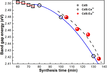
Figure 9 It shows band gap energy as a function of synthesis time for three samples series that were estimated by transmittance.
Figure 10 shows the photoluminescence spectra
of the undoped CdS for four different synthesis times. Figure 11 shows the photoluminescence spectra the deconvolution
of three typical samples (M65, M100 and M115). For sample M65, which presents best
luminescence of undoped films, the radiative bands are observed at 2.86, 2.37, 2.19,
1.88 and 1.38 eV that are labelled by a, b, c, d and e in the PL spectrum for a
better discussion, see Fig. 11A. The band a is
associated a radiative transition band-to-band, which is higher than the undoped CdS
band gap for 366 meV. This is due to the quantum confinement associated with grain
size since it is less than the excitonic Bohr radius. The band b is clearly
identified on as-grown CBD-CdS at 2.37 eV, which is called the optical signature of
interstitial oxygen38. Its
relative intensity increases with the synthesis time until it reaches a maximum at
65 min and then decreases for longer times, as is observed in figure. It has
reported that in samples grown by close-spaced sublimation (CSS) technique the
effect of oxygen is different since the use of oxygen during the growth leads to the
appearance of a band at 2.2 eV38.
The band c could be attributed to the CdO complexes that would be formed during the
growth due to the presence of oxygen during the nucleation of the layer, since the
CdO band gap is about 2.16 eV39.
For four studied CBD-CdS samples, another broad band, band d, is observed around
1.88 eV, this band named the “orange band” has been observed between 2.03-2.08
eV40,41, it is possibly associated to a
donor-acceptor pair (DAP) radiative transition between a donor level related to
interstitial cadmium

Figure 10 It shows the photoluminescence spectra CdS for three nanofilms series: a) undoped CdS, b) Eu-doped CdS and c) Ce-doped CdS.
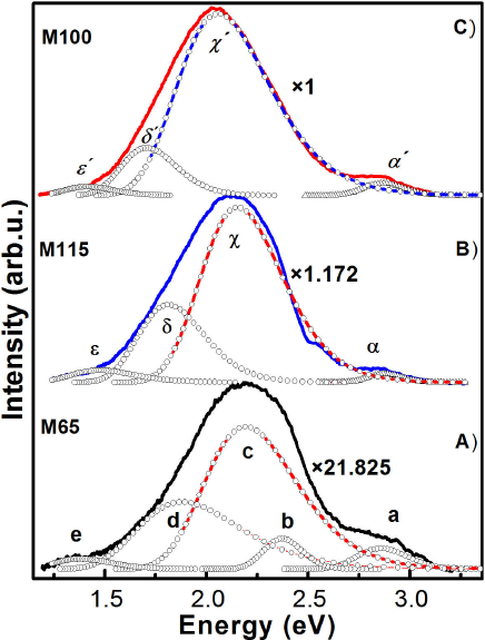
Figure 11 It is illustrated the PL deconvolution of the CdS nanofilms that presented the most intense photoluminescence: A) M65 sample, B) M115 sample and C) M100 sample. Additionally, it is shown the passivation factor associates to incorporation rare earth.
In addition, Fig. 11 shows the comparison of the photoluminescence spectra of the three samples with the best luminescence results, undoped and doped with rare earths CdS. It is clearly observed that the intensity of the PL spectra of doped CdS increases considerably, indicating that there is a passivation of the surface state density of the nanocrystals, but their dominant band redshifts.
4. Conclusions
In this work reported the growth successfully of (Eu3+,Ce3+)-doped CdS nanostructures synthesised by chemical bath deposition technique at different synthesis times and at 70 ±2°C. The crystalline structure of the nanostructures was zincblende type (111) direction, which was obtained by X-ray diffraction and Raman spectroscopy. The incorporation of rare earths in the CdS lattice was confirmed by EDS and X-ray diffraction. The nanocrystal size was determined by the Debye-Scherrer equation from ZB (111) direction, which was ranged from 2.35 to 2.67 nm for the CdS and 1.84-2.33 nm for rare earth-doped CdS that was confirmed by TEM. These grain sizes confirmed the quantisation effect in the synthesized samples due to are lower than the exciton Bohr radius. The RE-doped CdS exhibits a direct band gap that slightly decreases with increase of the synthesis time, from 2.50 to 2.42 eV, which was obtained by transmittance measurements. The room temperature photoluminescence of the undoped CdS presents the band-band transition associated to CdS nanocrystals size and the radiative transitions associated with residual impurities and structural defects, mainly the optical signature of interstitial oxygen. The photoluminescence of samples doped with europium present the band-band transition, in addition the radiative band associated to the intra-4f radiative transitions of Eu3+ ions that corresponds to the magnetic dipole transition (5D0 →7F1 ). For the case of cerium-doped samples, the results obtained were similar to those for europium. The results confirm that at least a part of the Eu3+ ions is effectively doped into CdS nanocrystals and the energy transfer occurs from CdS nanocrystals to Eu3+ ions. It was observed that the nanostructure, crystallite size and the band gap of the europium and cerium doped CdS nanocrystals can be finely controlled by simply varying the synthesis time. The passivation of the CdS by rare earths was approximately of an order of magnitude obtaining better results with cerium.

