


 text new page (beta)
 English (pdf)
 Article in xml format
 Article references
 Send this article by e-mail
 Cited by SciELO
  Similars in
SciELO
Similars in
SciELO 
 Permalink
PACS: 81.07.Bc; 81.15.Lm; 71.55.Gs; 82.20.-w; 83.85.Hf; 87.64.kp
1. Introduction
With the renewed interest of the nanostructures and nanoelectronics, materials studied extensively as CdTe, ZnTe, and its ternary alloy have also returned to be of interest in their nanometric form. In addition, these materials are explored in combination with the III-V semiconductors compound using these last as substrates. III-V semiconductors compound have showed to have large important optical characteristics, so they have found a wide field of applications for radiation and detection as is the case of GaAs and GaSb used as substrates in the present work. From the above pointed out, the main goal is to take advantage of the properties of ZnTe and CdTe nanolayers in combination with the III-V compounds when are used as substrates.1-4. In the case of its ternary alloy, the Cd1-X ZnX Te (CZT) band gap energy can be modulated from 1.45 to 2.25 eV, property that can be used for designing a large variety of radiation detectors 5,6. In addition, the layers with nanometric dimensions can be obtained with relative not complex growth techniques as is the case of the known as atomic layer deposition, which can be implemented using high purified hydrogen combined with a vapour phase deposition of the precursors on the substrate. So, it is not only an interesting issue but also and relative inexpensive way of obtaining nanolayers for future optical device fabrication.
2. Experimental procedures
Growth system: As is known, the ALD is a vapour phase technique based on the sequential saturation of the growth surface. It is tightly related with the CVD and PVD growth techniques. This growth technique was developed by Suntola and Antson in 19777 for depositing ZnS, and it was known as Atomic Layer Epitaxy (ALE). Nowadays due to the great success of nanomaterials and nanostructures, this technique, has been extensively studied, the amount of materials that can be deposited has been increasing. Literature about ALE includes a large number of papers and reviews7-13 As main characteristics of this growth technique is the excellent control of the thickness of the grown layers, determined by the number of exposition of the growth surface to the precursor vapours. In addition, the nature of the vapours and the number of allowed sites for the molecules or atoms on the substrate surface limits the grown layer thickness. In the case of samples presented in this work, when the growth surface is finished with Zn atoms (cations) the next layer Te (anion) is grown. For this growth type exists a set of conditions that are considered as a window for the growth parameters. The growth technique employed in this work is known as “isothermal closed space” this has been reported by other authors14. In summary, the growth system used in the experiments is an adaptation of a LPE system with the graphite boat adapted for the solid precursors, and the heater system and the gas system conserved, as is illustrated in Fig. 1. It has a horizontal geometry; the body of the reactor is made of a quartz tube while the suceptor is made of high purity graphite. The experiments were carried out using a high purity Pd-diffused hydrogen flow of 300 ml/min at atmospheric pressure. The substrates were exposed alternatively to the precursor vapours by sliding the graphite rule containing them. The elemental precursor vapour arrives on the substrate surface from little quartz tubes where are contained the precursors. In this way both of them, the anion flux and the cation flux saturate the growth surface one after the other making the process self-regulated. All, the graphite suceptor, substrates and precursor sources were maintained at the same temperature during the growth process. The graphite rule with the substrates is coupled to a step motor controlled by a computer program. This motor is located outside of the growth chamber. The computer program allows sequencing the layer growth and provides the desired exposure times. This system allows growing samples with more than 800 layers. The procedure employed for growing the CZT structure in this case, was based in the use of a cation source prepared making a mixture of Cd and Zn, combined by weights. Different weight combinations give different molar composition in the final grown layer.
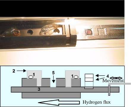
Figure 1 Details of suceptor used for growing the samples. In the upper part the photograph of the used boat is shown and the bottom part is the suceptor diagram, which is constituted of 1) Elemental source, 2) quartz container, 3) slide strip holder, 4) GaAs and GaSb substrates, and 5) purge hole. All components are into the quartz chamber with a constant flux of purified hydrogen.
Substrate preparation: The layers were grown on (001) oriented GaSb and GaAs substrates. The substrates preparation was as usually; degreased with organic solvents, oxide elimination using HCl followed by a chemical polishing. In the case of the GaAs substrate the used etching solution was H2SO4:H2O2:H2O, 5:1:1, while for the GaSb substrate was used a solution based in tartaric acid, hydrofluoric acid and hydrogen peroxide15. After the chemical etching, the substrates were rinsed in deionized water and then dried by blowing nitrogen onto their surfaces. As next step, the substrates were introduced into the growth chamber and were placed side-by-side on a graphite rule. In order to guarantee the same growth experimental conditions on both GaSb and GaAs substrates, the two substrates were loaded simultaneously at the same growth run. This was accomplished cutting rectangular substrates of 0.5×1.0 cm and placing them side-by-side to form a 1.0×1.0 cm substrate. In this way were eliminated possible factors produced by nonintentional variations in the growth processes assuring the same growth experimental conditions for the epitaxial layers on both substrates and allowing the direct comparison between the layers grown on GaSb and GaAs substrates. The experiments were carried out using a high purity Pd-diffused hydrogen flow of 300 ml/min at atmospheric pressure.
Sample characterization: In order to study the characteristics of the grown
epitaxial layer with temperature and thicknesses, high-resolution X-ray diffraction
(HR-XRD) measurements were performed. All diffractograms were acquired using a
Philips Analytical diffractometer. The parameters used for scanning were Cu
Kα1 line,
2.1. ZnTe growth procedure
The ZnTe layers were grown in a wide range of temperatures; however, ZnTe nanolayers with a shiny mirror-like surface could be grown at temperatures between 370 and 410°C on both GaSb and GaAs substrates. In the case of the GaAs substrates, at temperatures higher than 410°C the layer surfaces were deteriorated and showed a hazy appearance, but on GaSb substrates the layer surface remains shiny even at temperatures near at 420°C. In other series of experiments, the exposure times to the Zn and Te vapour sources were explored to determine the shortest exposure time that could be used for growing these layers. From these experiments, it was found that for exposure times less than 2.5 s there was no growth on the GaAs substrate, while in the case of GaSb substrate the shortest time was found to be 1.5 s for 385°C. This difference in the exposure times indicates that the growth kinetic is different for GaSb substrate compared with GaAs substrate. Additionally, these exposure times are not determined by the transport of the reactants on the growth surfaces. After the experiments with the exposure times, it adopted 3.0 s for growing the follow samples, and 3 s for the interruption time, as other researchers have reported 16.
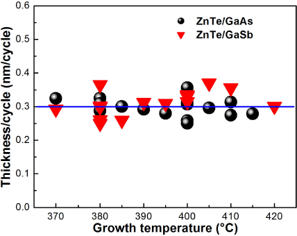
The ZnTe layers thicknesses were evaluated by ellipsometry measurements. The normalized results are summarized in Fig. 2, in this figure the presented layers were grown using different number of surface exposition to the element vapours; from 300 to 900. The horizontal scale corresponds to the growth temperatures explored in the experiments. In the same figure, can be observed that the average value of the thickness is in dependence of the number of surface exposition which was around 0.3 nm that is the value corresponding to a monolayer of ZnTe. This indicates that the growth regime is the known as Atomic Layer Deposition (ALD). As mentioned earlier, this growth regime allows to have a very good control on the layer thickness due to tight dependence of the final thickness on the growth cycles performed.
2.2. AFM Surface Morphology
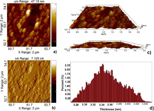
In order to explore the samples surface morphology, AFM topography images were taken, the results of these are illustrated in Fig. 3. In some cases, the AFM images present some structures as artifacts due to the tip adherence and contamination. The vertical scale is presented in nanometres, in the case of the 3D images can be observed that the maximum height is around 20 nm in the analysed area, which was
3. ZnTe high-resolution X-ray diffraction
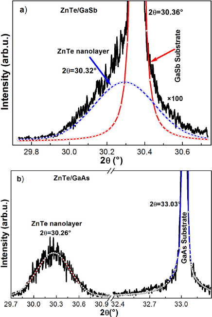
As result of the HR-XRD measurements, the peak corresponding to the (004) diffraction plane of ZnTe was identified and investigated. In Fig. 4, the thin peak about 33° corresponds to the (004) diffraction plane from the GaAs substrate, which was used as reference for the ZnTe layer peak position adjustment and its comparison. The wide peaks at the left of it, correspond to the (004) diffraction planes from the epitaxial layers, its intensities were amplified by 200 times due to the weaknesses of these peaks as a consequence of the thin thickness involved on the diffraction. The full width at half maximum (FWHM) of the diffraction peaks were very wide (600-800 arcsec) indicating a highly distorted lattice due mainly to mosaicity17. In addition, in this figure as is expected can be observed that the intensity of the peaks increases with the thickness of the layers. Moreover, as the layer thickness increases, the peak position shifts away from the peak corresponding to GaAs substrate towards the position that must have the corresponding to the ZnTe in bulk. This effect could be attributed to the relaxation of the layers and the increase of dislocation defects in the interface due to the fact that for highly dislocated layers the peak position is determined by the mean distortion of the lattice18. For the samples whose diffractograms are showed in Fig. 3 the calculated thicknesses were ranged between 135 to 270 nm.
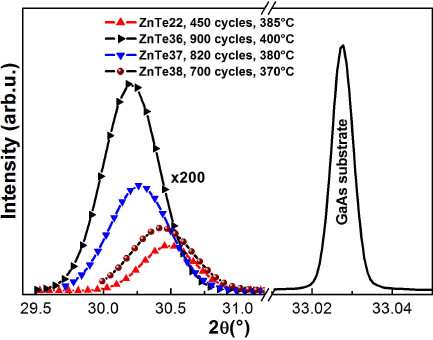
In the case of ZnTe layers grown on GaSb was not possible to resolve clearly the ZnTe diffraction peak from the one corresponding to the GaSb substrate. This is a consequence of the smaller lattice mismatch between the ZnTe layer and the GaSb substrate since the lattice constants of the two materials are very close,
4. Characterization by ZnTe Raman spectroscopy
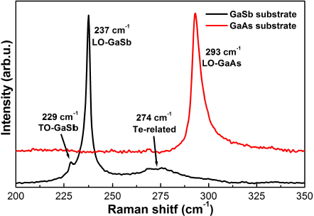
Back scattering geometry has been used to record the Raman spectra of the (100) GaSb and GaAs substrates that are shown in Fig. 6. GaSb Raman spectrum presents a dominant band at 237 cm-1 that is associated to longitudinal optical phonon (LO) frequency of GaSb, and other that is related to metallic tellurium observed at 274 cm-1 that was found experimentally. The weak shoulder on the low-frequency side of the GaSb-LO band at 229 cm-1 is the GaSb-TO mode, in principle forbidden in this experimental geometry. Its weak intensity in the Raman spectrum indicates that the crystalline quality of the Te-doped GaSb substrate is very good. Similarly, to GaAs substrate, which only shows a Raman peak at 293 cm-1 that is associated with GaAs-LO mode. Raman scattering measurements were made to the substrates used to have a reference if there had been thin film growth on different used substrates.
For assessing the quality of the ZnTe grown layers Raman spectroscopy measurements were performed. The obtained results are shown in Fig. 7. As was mentioned above the measurements were carried out at room temperature on samples (001) oriented at normal incidence. It is noteworthy that first and second order Raman dispersion was obtained of the grown samples. The TO-ZnTe mode is forbidden in the experimental measurement configuration geometry for (001) substrate orientation, which becomes active by the breakdown of the selection rules in the backscattering configuration. This breakdown is attributed to the generation of structural defects as misfit dislocation in the layer-substrate interface and other crystallinity problems originated from compositional fluctuations and by elastic scattering from ionized doping impurities. In Fig. 7 are shown the Raman spectra of samples grown on GaSb and GaAs substrates. Fig. 7a illustrates the deconvolution of two Raman spectra, which present first and second order Raman scattering of the ZnTe, the frequencies of these peaks are shown in Table I. In these ones, there are two dominant peaks, corresponding to the tellurium related bands around 123 and 141 cm-121-23. The discussion of Raman scattering will be divided into two, corresponding to the Raman of first-order and second-order.
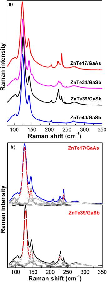
Figure 7 a) ZnTe Raman spectra of samples with different thicknesses and substrate. b) Decomposition of the measured Raman spectra into individual components for two samples grown in different substrates GaAs and GaSb. The circles lines are their respective fitting.
Table I Frequency of active Raman lines detected for the ZnTe samples grown on the two different substrates32.
| Order Raman | Mode assignation | GaAs | GaSb |
| First | Te2O-related | 126 | 128 |
| Te-related | 144 | 146 | |
| LO-ZnTe | 208 | 208 | |
| Second | 2TA(L)-ZnTe | 96 | 96 |
| 2TA(X)-ZnTe | 105 | 106 | |
| (W1+W2)-ZnTe | 159 | 159 | |
| (TO(X)+TA(X))- ZnTe |
226 | 228 | |
| (LO(X)+TA(X))- ZnTe |
238 | 238 | |
| 2LA(X)-ZnTe | 273 | 275 |
First-order Raman. ZnTe has a crystal structure of the zincblende type with two atoms per unit cell. Thus, it would expect three degenerate optic modes of vibrations at the centre of the Brillouin zone (q=0); however, the binding is partially ionic and in this case Poulet24 has shown that the macroscopic electric field associated with the longitudinal mode of vibration increases its frequency above that of the transverse mode of vibration. The first-order Raman spectrum consists of two bands: The highest in frequency is associated to the longitudinal optical (LO) branch and the lowest is the doubly degenerate transverse optical (TO) branch. Thus, the peak observed at 208 cm-1 corresponds to the ZnTe longitudinal optical phonon25-28. The Raman spectra exhibit peaks related to the substrate characteristics. For the ZnTe Raman spectrum of the layers grown on the GaSb substrate, it can be observed three dominant peaks between 90 and 150 cm-1 that are associated with Te. As in the case of samples grown on GaAs substrate the peak at 208 cm-1 corresponds to LO-ZnTe26,29. In addition, as can be observed in figure is evident the weakness of the peak corresponding to LO-ZnTe and is slightly displaced in comparison with the reported for the ZnTe in bulk, possibly due to the layers stress and the nanometric nature of these layers, as has been reported by other authors23. In the second-order scattering process, the energy of the scattered photons differs from the energy of the incident photons by the energy of two vibrational quanta. The two phonons involved can be from the same branch (overtones) or from different branches (sums or differences). The wavevector of the phonons involved is usually orders-of-magnitude larger than that of the photons and conservation of crystal momentum therefore requires that the wavevectors of the two phonons be equal and opposite in sign. Thus, the two phonons involved, although they may be from different branches of the spectrum must come from the same point in the zone. This of course is still allow, two phonon scattering from any point in the zone and the scattered spectrum will consist of a continuous background with peaks corresponding to critical points in the two-phonon density of states30.
The critical points in the zinc blende phonon spectrum31 are at the points
5. CdTe X-ray diffraction characterization
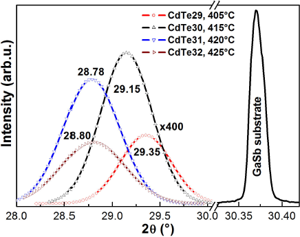
In the case of CdTe samples, these were grown on (100) oriented GaAs and GaSb substrates as in the ZnTe layers case, although the range of growth temperatures for the CdTe deposition was slightly different. Temperatures higher than 400°C were necessary for the CdTe growth. As in the ZnTe case, the exposure time under the vapour sources was selected as 3 s.
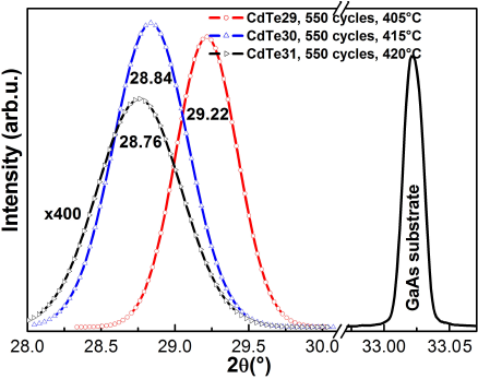
The explored temperature range used for growing the samples is presented in Fig. 8; these were higher than 400°C and lower than 430
6. CdTe Raman scattering measurements
Figure 10 shows the Raman spectra for CdTe nanolayers excited by 532 nm wavelength light. Two Raman spectra were fitted with Lorentzian peaks (black circles) that are shown in Fig. 10b. The peaks at 95-98, 120-125 and 140-143 cm-1 have been identified from trigonal Te33. The 120-125 cm-1 peak is due to a phonon with A1 symmetry and the 95-98 and 140-143 cm-1 peaks originated from phonons with an E symmetry35. However, the 140-143 cm-1 peak could also be assigned to the TO phonon in CdTe because of it is very close to one as reported31,33. According to Raman studies of CdTe33,36 the peak located at 157-160 cm-1 can be assigned to the LO phonon of CdTe, in spite of a difference from 171 and 167 cm-1 reported by Islam et al.37 and Amirtharaj et al.33, respectively. In order to the best of our knowledge, there have been no reports of the assignment for the broad band located at 265-270 cm-1, which probably originate from combination bands and we tentatively assign them to the overtones of E and A1 modes in Te. The 295 cm-1 peak could be assign at LO-GaAs. The peak at 321 cm-1 is associated with the phononic replica of the longitudinal optical mode of the CdTe38. A high concentration of tellurium exists in the as-prepared CdTe nanolayers, as shown by the Raman study39. Similar phenomena were reported in CdTe film synthesized through the liquid-phase epitaxy method37 as well as the surface of single crystal CdTe in bulk form33. One possible explanation could be that the free energy of Te is smaller than that of CdTe and thus Te crystals can easily form during the synthesis of CdTe. However, further study is still needed to confirm this one. One implication for this is that the surface property of the nanolayers may not be as expected. Isolated elemental domains (Te) are formed or precipitated on the surface of nanolayers; it may affect their applications in optoelectronic devices since its elemental properties are different from its compound properties.
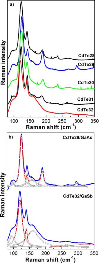
Figure 10 a) CdTe Raman spectra of samples with different thicknesses and substrate. b) Decomposition of the measured Raman spectra into individual components for two samples grown in different substrates: GaAs and GaSb. The circles lines are their respective fitting.
7. Cd1-X ZnX Te growth
After successfully obtaining the ZnTe and CdTe layers, it was proceeded to grow the layers of
the Cd1-X
ZnX Te ternary alloy, which was grown on (100)
oriented GaAs substrates. The used temperature range was between 400 and 425°C. In
order to grow the layers was used as precursor a solid source prepared by weighing
the corresponding amounts of zinc and cadmium and mixing them. The procedure for
preparing the precursor source was accomplished by combining Zn and Cd in different
amounts and then were melted into a liquid form at high temperature and then this
liquid was cooled rapidly for its solidification to form a new solid. The resulting
solid was used as the cation precursor source. Its vapour pressure was controlled by
controlling the temperature. For the samples studied in this work and shown in Fig. 11 were used the combinations of Zn and Cd
weights presented in Table III in which, the
column labelled by “x in the grown layer” represents the final
molar composition of solid Cd1-X
ZnX Te layers. The molar composition of these
layers was evaluated using the Vergard’s Law
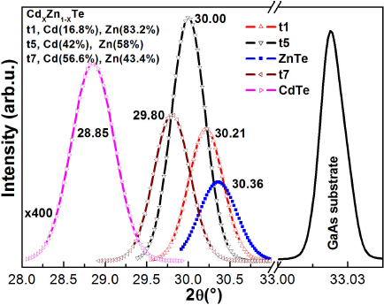
Table III Cation source composition used for growing the ternary Cd1-X ZnX Te
| Sample | Solid sources composition (%) |
x in the grown layer (%) |
|
| Zn | Cd | ||
| T1 | 83.2 | 16.8 | 92.5 |
| T5 | 58.0 | 42.0 | 90.0 |
| T7 | 43.4 | 56.6 | 89.7 |
So, from these results can be concluded that different molar concentration of Zn in the layers of the ternary alloy can be obtained, preparing the solid precursor source with different Zn and Cd combination. In the presented samples, the Zn molar composition was varied from 83.2 to 43.4% but the variation of the molar composition of the grown layer was from 92.5 to 89.7%, respectively. The full-width half-maximum (FWHM), of these peaks are above 3600 arcsecs, that can be considered large and can be attributed to mosaicity, combined with the nanometric dimensions of the layers, and to the generation of misfit defects.
8. Conclusions
In this work we reported the successfully growth of ZnTe on both GaAs and GaSb substrates by the Atomic Layer Deposition regime as was shown from the thickness measurements performed by ellipsometry. In addition, CdTe and the ternary alloy Cd1-X ZnX Te were grown successfully by the same growth method by preparing a mixture of cadmium and zinc, and then melting it was possible to form a solid for growing the Cd1-X ZnX Te alloy. The molar quantity x of the grown layer was varied modifying the composition of the solid used as cation source. X-ray diffraction shown a dependence of the (004) diffraction peak position with temperature and with the sample thickness which can be attributed to the lattice relaxation produced by the increase of defects. In addition, Raman characterization shown that the samples obtained presented Te inclusions and a large density of defects possible dominated by misfit dislocation.

