


 nueva página del texto (beta)
 Inglés (pdf)
 Artículo en XML
 Referencias del artículo
 Enviar artículo por email
 Citado por SciELO
  Similares en
SciELO
Similares en
SciELO 
 Permalink
PACS: 81.05.Ea; 81.15.Gh; 81.07.Gf; 81.10.Aj.
1. Introduction
In the past decade, nanostructures have drawn great attention due to their importance in fundamental research. Scientific researchers all over the world have developed numerous semiconductor devices based on one-dimensional nanostructures such as nanowire 1,2,3,4 and nanotube5,6. Because of their large surface-to-volume ratios, the quantum confinement size regime and surface states, nanowires and nanotubes have been proved to be excellent building blocks of nanoscale electronic, optoelectronic, electrochemical and electromechanical devices 7,8,9. Additionally, one-dimensional nanostructure tends to be free of dislocation and single-crystalline while growing 10.
Aluminum nitride, an important material for electronic and optoelectronic devices, exhibits the largest band gap of 6.2 eV among III-nitride compounds 11, small electron affinity ranging from negative to 0.6 eV 12, high piezoelectric response 13 and excellent thermal conductivity 14. Due to these properties, aluminum nitride is a promising candidate for applications such as deep-ultraviolet light-emitting diodes (LEDs), high-power/high-frequency electronic devices, field emitters and piezoelectric devices. However, the development of this material has been limited by its insulating property and the difficulties in growing high crystalline AlN 15.
To date, although, some 1D AlN nanostructures have been synthesized by a few routes, there must be much effort to develop new techniques for synthesizing AlN nanostructures in simple way and at lower temperature. Among now available routes, physical vapor transport requires an extremely high growing temperature because of the refractory character and low vapor pressure of AlN 16,17. Moreover, molecular beam epitaxy is difficult to synthesize nanowires in quantity. Here, we demonstrate a direct growth of AlN nanowires via the reaction between Al and NH3 with Ni as catalyst. We obtain different morphologies of AlN nanostructures by tuning the growth temperature and growth time.
2. Experimental
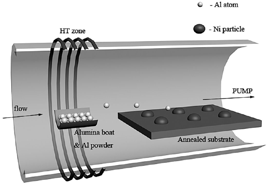
The AlN nanowires were synthesized by chemical vapor deposition on Si (100) substrate. The Si substrate was cleaned by acetone, ethanol and de-ionized water sequentially with ultrasonic bath to remove residual contaminations on the surface. Ni film was deposited on the Si substrate by RF magnetron sputtering. The Ni-coated Si substrate was located about 3 cm downstream to the Al powder (99.95%) in an alumina boat and both were placed in a tube within a furnace. The tube was flushed with N2 for 20 minutes to remove oxygen and moisture. Then, the furnace was heated to 1050°C at a rate of 25°C/min and kept for 10 min under the flowing N2 of 80 sccm. This process aimed to transform Ni film to nanodots. After that, the temperature was changed to a desired growth temperature, N2 flow was replaced by NH3 with the flow rate of 60 sccm. The desired growth temperature was maintained for 15 or 30 minutes. Finally, the system was naturally cooled down to room temperature. AlN products were obtained on the Si substrate. The reaction chamber is shown in Fig. 1.
The products were characterized by scanning electron microscopy (SEM; JSM-6700), transmission electron microscopy (TEM), X-ray diffraction (D8X) and X-ray photoelectron spectroscopy (XPS).
3. Results and discussion
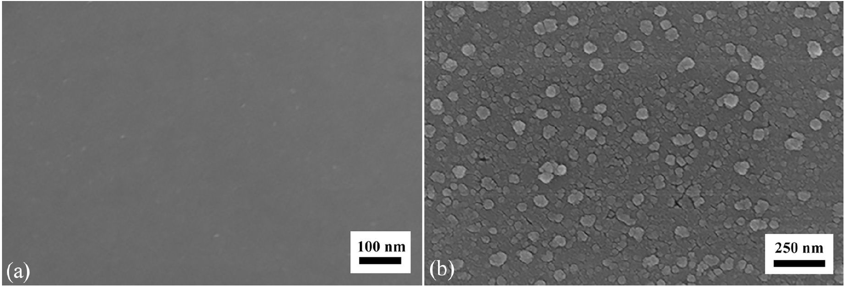
At the beginning of growth, the nickel thin film must be annealed. The ideal situation is to keep the nickel catalyst as droplet in nanoscale. The Ni film was annealed at 1050°C for 10 min in nitrogen in order to avoid introducing impurities into the samples. Figure 2 show the SEM images of unannealed and annealed substrate. It can be clearly seen that nickel has been transformed to catalyst islands. The size of nanoparticles varied in the range from 20 to 80 nm.
Typical SEM images of the as-prepared AlN nanostructures are shown in Fig. 3. These nanostructures were grown for 15 minutes with the flowing NH3 of 60 sccm under 1000°C, 975°C, 950°C, 925°C, 900°C and 875°C, which are corresponding to Fig. 3(a)-(f), respectively. Fig. 3(a)-(c) show the morphologies of the long nanowires. The particles visible at the top of the nanowires indicate that the growth of the nanowires is based on VLS mechanism. The nanowires are about 4-5 micrometers in length. By measuring, the diameter ranges of nanowires in Fig. 3(a)-(c) are 30-92, 20-60 and 14-60 nm and the average diameters are 52, 36, 28 nm, respectively. Fig. 3(d) shows the image of short nanorods. The diameter of these structures is about 30 nm and the length is only several hundred nanometers which due to the slower axial growth. There are particles on the tips of nanorods as well. The nanorods may be the early stage of the nanowires. In Fig. 3(e), only AlN clusters exist on the substrate and, in Fig. 3(f), there are Ni particles with a few nanorods. It indicates that temperature lower than 900°C is unfit for large-area fabrication of AlN nanowire.
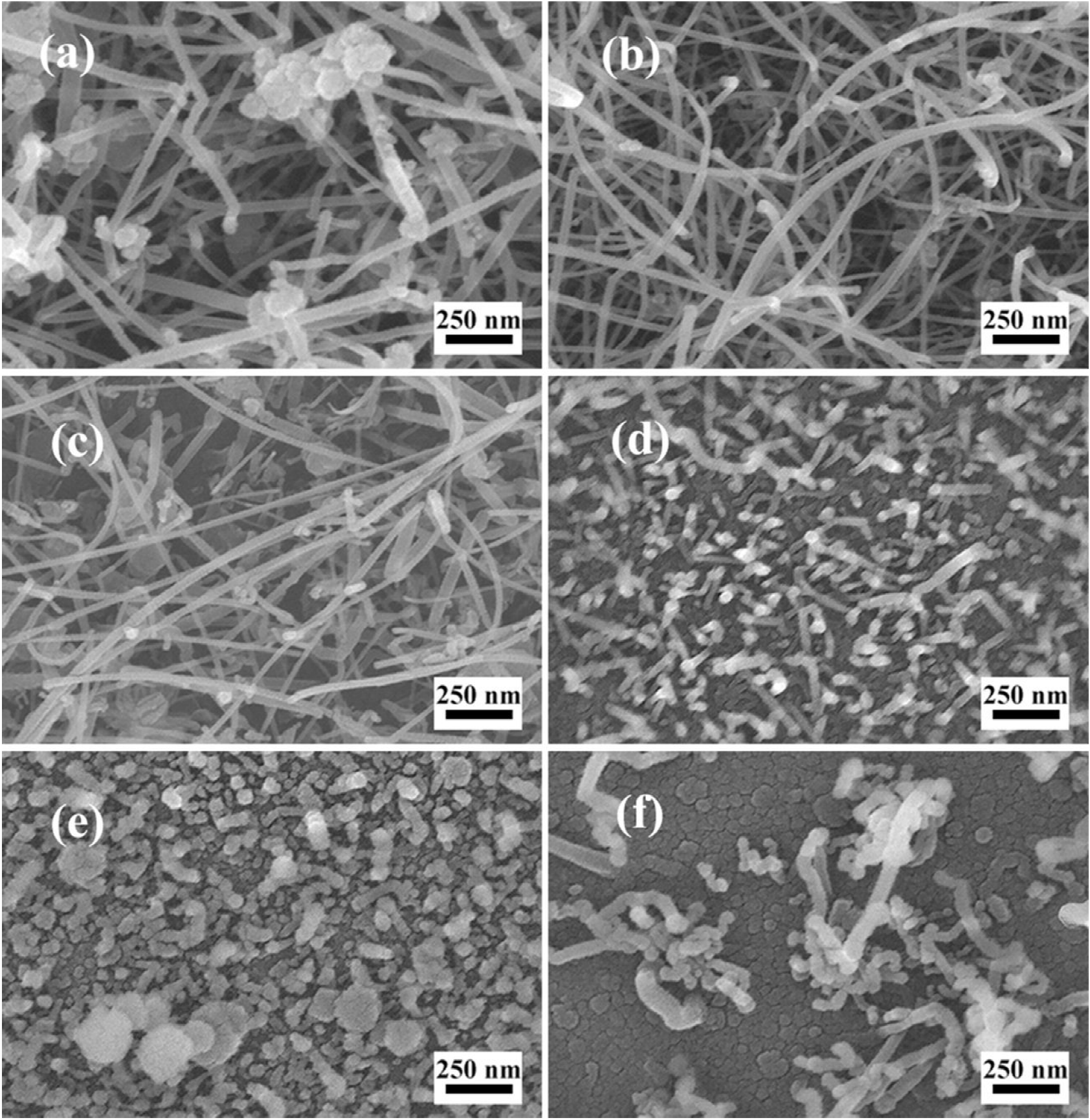
Figure 3. SEM images of the AlN nanostructures grown for 15 min under various temperatures (a) 1000°C, (b) 975°C, (c) 950°C, (d) 925°C, (e) 900°C, (f) 875°C, respectively.
It is found that as the growth temperature increases, the structures change from nano-clusters to nanowires. As for nanowires, at higher temperature, the average diameter is slightly larger. It can be explained as follow. When the temperature is too low, the reaction between Al and ammonia is too slow to form nanowire in the initial growth stage. While temperature increasing, once the nanowires generate, depositions on sidewall become easier to occur. However, at the temperature in our experiment, most atoms can diffuse along nanowire to catalyst. The lateral growth accelerates slightly.
To identify the component and structure of the product. XRD and XPS was employed. Fig. 4(a) shows the XRD pattern of nanowires grown for 15 min under 975°C. Four peaks of wurtzite AlN corresponding to (101), (102), (110), (103) plane with one peak corresponding to SiO2 (101) and one peak corresponding to Al2O3 (400) can be observed. In XPS measurement, the C1s binding energy of adventitious carbon (284.8 eV) was used to calibrate the energy scale. The pattern in Fig. 4(b) reveals that the binding energy of N1s in prepared nanowires is about 397.0 eV which can be consistent with the value of AlN. The binding energy of Al2p shown in Fig. 4(c) is identified at 74.5 eV which is close to the value of Al2O3. We think the product is wurtzite AlN with slightly surface oxidization. Due to the aluminum powder left on the surface of product and substrate, while the furnace was cooling down, it’s easy to yield Al2O3.
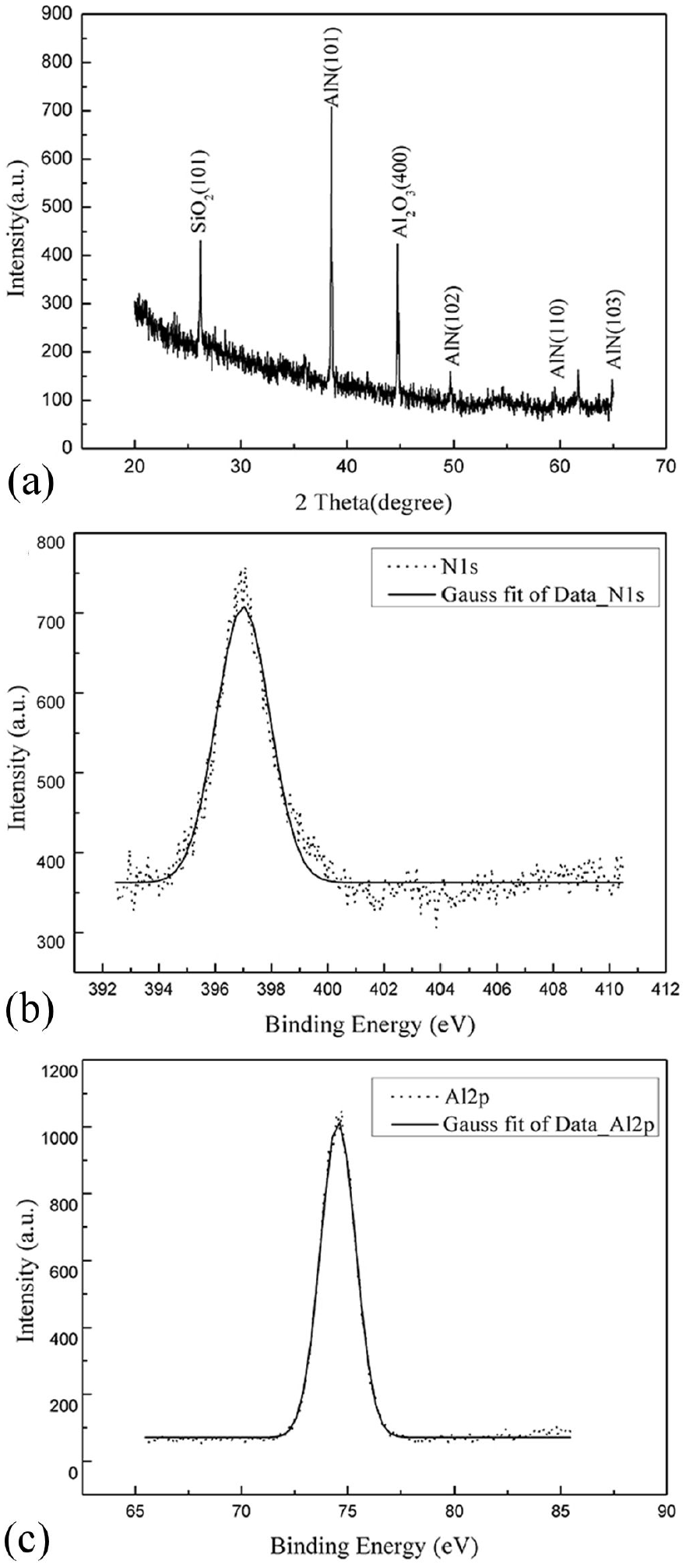
Figure 4. (a) XRD pattern of nanowires grown under 975°C. XPS patterns of nanowires grown under 975°C, (b) the binding energy of N1s, (c) the binding energy of Al2p, respectively.
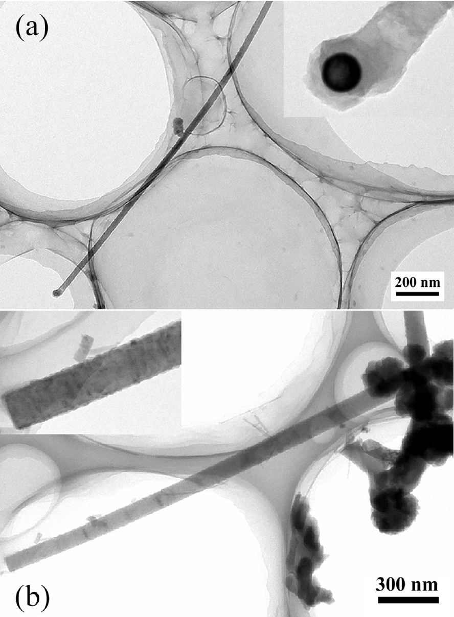
The morphology of the nanowires has been further analyzed by TEM. Fig. 5(a) shows a nanowire grown at 1000°C. In the inset, a particle shows on the tip of the nanowire which exhibits a different contrast and can be morphologically identified. Considering the materials participating in our experiments and our previous works, the particle is probably the residuary catalyst. The diameter of the nanowire is about 35 nm. The diameter of the particle is 20 nm which is much smaller than the nanowire’s. Fig. 5(b) shows a nanowire grown at 975°C. The diameter of the nanowire is about 100 nm. These two typical morphologies have been found in all samples where nanowires are observed.
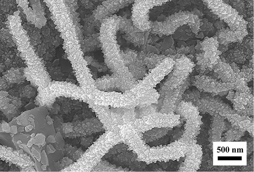
To investigate how the growth time affects the morphology of nanowires, we obtain the SEM image of sample grown under 950°C for 30 min in Fig. 6. Compared with the sample grown for 15 min, the lateral growth of the nanowires accelerates. What’s more, the surface of the nanowire become rougher which may indicate that the lateral growth of nanowires is strongly influenced by VS growth.
In Wu and Peng’s paper 18 published in 2015, they have synthesized high-quality, large-scale wurtzite AlN nanowires on c-Al2O3 substrates using a catalyst-assisted chemical vapor deposition method. Compared with their work, we synthesized AlN nanowires on Si (100) substrates and studied how the temperature and growth time affect the growth of AlN nanowires. While their work shows that the VLS mechanism is dominant in the nucleation and growth of AlN nanowires via the catalyst-assisted CVD process, our work demonstrates that the growth of the nanowires is based on both VLS and VS mechanism. The morphology evolution of nanowires in our samples demonstrates that the initial growth is based on VLS growth and the VS growth progressively dominates.
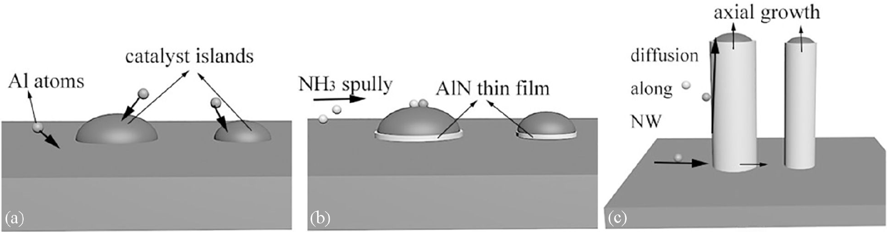
The growth mechanism for AlN nanowires in our experiment can be proposed. The schematic diagram was provided in Fig. 7. For AlN nanowires, the annealed nickel islands act as catalyst to dissolute the precursors and provide the nucleation and growth site for nanowires 19. Al atoms introduced by the carrier gas from the evaporation source start to diffuse on the surface of the catalyst islands shown in Fig. 7(a). When the NH3 flow is supplied and the temperature is suitable, the supersaturation at the L-S interface led a thin AlN layer form in the initial growth stage as Fig. 7(b). With the precursors supplied continuously, in this stage, most reaction species are directly absorbed by catalyst particle or diffuse along the nanowire to the L-S interface where deposition occurs. It means that axial growth dominates. When the nanowires grow longer than the average diffusion distance 20 of precursor atoms or the nickel islands become too small to act as catalyst, more atoms cannot reach to the L-S surface and rough surfaces on which deposition of atoms is relatively easy start to generate at the sidewall of nanowire. When growth continues, the lateral growth rate which is based on VS mechanism will be greater than the axial growth rate. So, when the growth time increases, nanowires are larger in diameter with rough surface. Therefore, preparing large catalyst islands is the key to synthesize high quality AlN nanowires.
4. Conclusion
In summary, the AlN nanowires were synthesized by CVD through the direction reaction of Al and ammonia with Ni as catalyst. With different growth temperature between 1000°C to 875°C, the different morphologies of AlN nanostructures were obtained. In our works, the AlN nanowires could hardly growth under the temperature lower than 900°C. XRD pattern and XPS patterns demonstrate the wurtzite AlN were synthesized with slightly surface oxidation. Base on the evolution of the nanowires with different growth temperature or growth time, the growth mechanism has been proposed for the AlN nanowires. The initial axial growth of nanowires is based on VLS mechanism while the VS mechanism progressively dominates the growth as the growth time increases to form a rough surface. The work is helpful to achieve the fabrication of AlN nanostructures with Ni catalyst and to understand the growth process of nanomaterials.

