


 nueva página del texto (beta)
 Inglés (pdf)
 Artículo en XML
 Referencias del artículo
 Enviar artículo por email
 Citado por SciELO
  Similares en
SciELO
Similares en
SciELO 
 Permalink
1. Introduction
Metal oxide semiconductor films have been widely studied and have received considerable attention in recent years. Particularly ZnO films have great potential applications in light-emitting diodes1, field-effect transistor2, flat panel display3, ultraviolet lasers4, sensor5 and solar cells6, due its properties such as piezoelectric, wide and direct band gap of 3.37 eV and a large exciton binding energy of 60 meV, transparent conductive oxide principally. A lot of methods have been extensively used for oriented ZnO films synthesis, including L-MBE7, pulsed laser deposition8, metal-organic chemical vapor deposition7, cathodic magnetron sputtering7-10 and reactive electron beam evaporation11-15, spray pyrolysis16-19, chemical vapor deposition (CVD)20, and electrodeposition21,22. However, sol-gel processes are particularly adapted to produce ZnO colloids23 and films24-25 in a simple, low-cost and highly controlled way. ZnO thin film synthesis by sol-gel method involves several parameters: (1) the nature of the precursor and its concentration, (2) the type of solvent and the acidity of the medium, (3) the type of additive species and their concentrations, (4) the aging time of the early mixture, (5) the method of coating of substrates and its speed, (6) the nature of the substrate, and (7) the pre-heat treatment and temperature annealing of the materials. A survey of the literature shows that all these parameters play a key role on the evolution of texture in zinc oxide film, however, the temperature annealing affects overall film quality, and therefore, the temperature annealing should be carefully chosen. Several authors mention that, the temperature range 500-700°C seems to be the most appropriate26,32. So it is difficult to find reports of heat treatment in the range of 600-1000°C in oxygen and nitrogen atmospheres.
The main objective of this work is to study the change in the structural characteristics, optical and electrical properties of ZnO films deposited by the sol-gel method and crystallized at 600, 800 and 1000°C in N2 and O2 atmospheres, temperature range employed in the based devices ZnO.
2. Material and methods
ZnO thin films were prepared using the sol-gel method, a solution was synthesized by dissolving zinc acetate dehydrate in 2-methoxyethano (2-ME), and then a stabilizer of monoethanolmine (MEA) was added to the blended solution. The molar concentration of zinc ions was 0.5 M, and the molar ration of MEA to zinc ions was maintained at 1:1. The solution was stirred for 30 min to yield a clear and transparent. All ZnO sol-gel films were spin-coated onto pre-cleaned silicon substrates at a rotations speed of 3000 rpm for 30 s. Each such coated film was heated at 300°C for 15 min to evaporate the solvent, water, and organics. The spin coating and drying procedures above described, were repeated ten times. Finally to achieve crystalline, ZnO films were annealed at 600, 800 and 1000°C for 2 hours in N2 and O2 atmospheres. The morphologic of ZnO films was examined by an X-ray diffractometer (Discover D8) with Cu-kα radiation (
3. Results and discussion
Following the sol-gel coating process, an XRD analysis was performed to investigate
the effect of different atmospheres and temperatures annealing on the crystal
structure of ZnO films. Figure 1 shows the XRD
pattern of ZnO films growth on the silicon substrates annealed in an atmosphere of
oxygen (O2) and nitrogen (N2) at temperatures of 600, 800 and 1000°C. The
XRD pattern shows there is a preferential orientation in the plane (002), with type
hexagonal wurtzite structure of ZnO, in all cases; however, for the samples annealed
at 600°C patterns show also preferential orientations of (100) and (101), this is
due to a lower crystallinity with respect to films annealed at 800 and 1000°C. In
ZnO films with heat treatment in O2 atmosphere, it is observed that the
crystallinity is increased with temperature33. In the case of films annealed in N2
atmosphere the behavior is similar, except for the samples annealed at 1000 ∘ C for
which intensity is diminished. Also, it was found that the intensity of (002)
diffraction peak increases and the full width at half maximum (FWHM) becomes narrow
with temperature and atmospheres annealing. The increase of diffraction intensity
and narrowing of FWHW are related to the enhanced crystallinity and increased grain
size. The grain size (D) was computed according to the Scherrer34 Eq.


Figura 2 Surface morphologic of the ZnO films deposited by sol gel method, the atmosphere annealing N2 (right), O2 (left) and annealing temperatures of (a,b) 600, (c,d) 800 and (e,f) 1000°C
A study of the photoluminescence property of ZnO films is very important because it can provide more valuable information on the quality and purity of the material. Figure 3 shows the PL spectra of annealed ZnO films. Two UV emission peak centered at 362 and 380 nm, and a weak blue emission at 405 nm were obtained for all the ZnO film. The strong and sharp emission in 382 nm corresponds to the transition from free exciton (FX). The intensity of this emission is related to ZnO films with higher quality crystalline36, this corresponds to the films annealed in O2 atmosphere at 800 and 1000°C and in N2 atmosphere at 800°C. The emission band centered at 362 nm is excitonic nature regarding donor or acceptor levels37. Finally, the emission at 405 nm (3.14 eV) is attributed to transitions related acceptor levels due to zinc vacancies, VZn or excess de oxygen,38. As seen in the case of annealing O2 at 1000°C.

Figure 4 shows the results of the Hall Effect measurements at 300 K, carrier concentration versus annealing temperature for two annealing atmosphere (Fig. 4a). Fig. 4a shows that 600°C annealing temperature versus the carrier concentration. In this graph shown, when the annealing temperature is 600°C has a higher carrier concentration for both atmospheres. This is related to the crystalline quality of the films and the grain size these are similar for two atmospheres annealing, and thus the intrinsic defects in the films are similar, and these values of n corresponds to a semiconductor degenerate39,40. When the temperature annealing increased to 800°C, carrier concentration decreases with respect at the annealed films at 600°C at both annealing atmospheres, this result could be associated with higher peak intensity X-ray diffraction of the plane (002)35, i.e., if the carrier concentration decreases, probably the tension on the lattice decrease and thereby improves the crystalline quality of the films. The value of the carrier concentration for annealing in N2 is greater this is due to desorption of O2, increasing the vacancies of O2 and therefore the value carrier concentration incremented38. For the annealing temperature of 1000°C, the value of the carrier concentration was increased for the annealing atmosphere at N2 due to increased of vacancies of O2, however for annealing atmosphere at O2 the value of the carrier concentration remains as the film annealed at 800°C. This result be associated with the spectra of X-ray diffraction, which showed that the crystalline quality decreases with annealing atmosphere at N2 and for the O2 is similar (in peak intensity and width FWHM). Figure 4b shows the mobility versus the temperature and atmosphere annealing. Shows that annealing temperature 600°C is low and mobility similar value for both annealing atmospheres, this due to the high concentration of carriers, so that there is a high dispersion of the evaporators for defects. When the annealing temperature was 800°C mobility increases according to the decrease in carrier concentration, being higher for films with the annealing atmosphere O2 in N2. Finally, to the annealing tem- perature of 1000°C is observed that decreases mobility for samples annealed at 800°C, again due to increased carrier concentration, even though the films are annealed at 1000°C less grain boundaries, as shown in Fig. 2 based on this result we can say that the dominant mechanism of scattering of carriers is due to defects not electrically activated and grain boundary scattering.
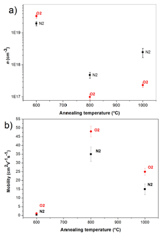
Figure 4 Carrier concentration (a) and mobility (b) of the ZnO films versus temperature and atmospheres annealing.
The conductivity versus 1/T characteristics of typical ZnO films in N 2 and O 2 annealing atmosphere are shown in Fig. 5. At temperatures values above 220 K, there are two possible transport carriers mechanisms, the thermally excited carriers from the conduction band from the donor levels and the carrier transport by thermionic emission due the grain boundaries41. For this temperature range, can coexist two transport mechanisms; however the dominant mechanism corresponds to the first mentioned above, because the emission via grain boundaries was not adequate. At temperatures below 220 K, various authors mention that the transport mechanism may be due to conduction through neighboring donor levels, however, there is no accordance in the literature Y. Natsume et. al.41 mentioned that can be obtained for values less than 200 K, P. Sagar et. al.39 suggests that this mechanism should occur at temperatures below 100 K. In this work the dependence of the conductivity as a function is according to 𝑇 −1/4 . Thus, the transport mechanism dominant could correspond to carrier transport through the conduction band from thermally excited donor levels, so that we can use the following expression:


Ea1 and Ea2 which correspond to the activation energies of donor levels, k the Boltzmann constant and σ1, σ2 preexponential factors. In Fig. 3.10, shows the slopes were the activation energy and the donor levels was obtained with respect to the conduction band (the donor level values are obtained from the relationship Ed1 = 2Ea1 and Ed2 = 2Ea2).
Values obtained donor level (Table 1) are similar to the results from films annealed at atmosphere of N2 and O2, according to the literature this corresponds to the presence of native defects such as zinc interstitial and oxygen vacancies or both 42. Similar values were obtained by several authors43-46.
4. Conclusions
In this work is shown that the structural optical and electrical properties are dependent to the temperature and the annealing atmospheres for the films obtained by this method. According to the XRD patterns the thin films shows 002 preferential orientation, where the intensity of the peak increases with the temperature except for the film annealing at 1000°C in atmosphere of N2 due of the desorption of O2.
The results show that the thin films exhibit a major cristallinity quality and have a high emission at UV band at room temperature and a weak emission in the visible region.
From the results obtained in the electrical characterization shows that the carrier concentration and the mobility depend directly of the temperature and annealing atmosphere. However the increasing of the annealing temperature causes the decreasing of the carrier concentration therefore the rise of the mobility. In this work the increase of the mobility depend directly to the values lower of the carrier concentration and the mechanism of the dispersion dominant are just by defects and not by the grain boundaries.

