


 text new page (beta)
 English (pdf)
 Article in xml format
 Article references
 Send this article by e-mail
 Cited by SciELO
  Similars in
SciELO
Similars in
SciELO 
 Permalink
PACS: 81.05.Dz; 81.65.Cf; 81.10.Pq
1. Introduction
CdTe is a very promising material for use in thin-films solar cells; its advantages as a solar cell absorber include its high optical absorption coefficient and direct bandgap of around 1.5 eV that is nearly ideal for optimal solar conversion 1. Now the highest efficiency of CdTe thin film solar cells is 21.5%, achieved by First Solar 2.
Post-deposition processing of polycrystalline CdTe/CdS hetero-junction thin films solar cells with cadmium chloride (CdCl2) heat-treatment has proved to improve the short circuit current and open circuit voltage of CdTe/CdS thin film solar cell by recrystallization, reorientation and grain enhancement of films for photovoltaic operation 3. Generally, the CdCl2 activation can be realized by two methods. The most typical CdCl2 methods are wet CdCl2 treatment with a CdCl2:CH3OH solution and vapour CdCl2 treatment. Wet CdCl2 treatment, which is applied after the deposition of a CdTe absorber layer and prior to the application of a back contact 4.
CdCl2 treatment has become a standard and critical process in the fabrication of high-efficiency CdTe based photovoltaic devices, considering that CdTe films would have many undesirable characteristics such as small grains, short minority carrier lifetime and high resistivity due to large number of grain boundaries. Regardless of the method used for depositing the CdTe layer. The fact that the CdCl2 treatment is necessary in polycrystalline CdTe due to the thickness of CdTe thin film decreased after CdCl2 heat treatment and the grain size increase 5,6. However, the exact roles of Cl in enhancing and even limiting CdTe solar cell efficiency are still under debate as many explanations and mechanisms have been proposed. As Ji-Hu Yang 3 found that Cl can either substitute Te atoms to form ClTe or form interstitial defects. CdCl2 heat treatment suggests that Cl may have strong interaction with CdTe grain boundaries (GBs).
In this work, hydrated-CdCl2 heat treatment effects on physical properties of CdTe thin film fabricated using CSVT have been investigated. The morphological analysis of the CdTe films and the influence of the annealing with hydrated-CdCl2 heat treatment on CdTe surface is investigated using SEM and correlated with EDXS and SIMS techniques, on the other hand the structural characteristics was analysed by XRD and state electronics was studied using photoluminescence at 14 K. Finally, the performance of CdTe solar cells using hydrated-CdCl2 heat treatment was analysed.
2. Experimental details of fabrication of solar cells
Soda lime glass, SnO2:F were used as substrates and front contact, CdS thin films were used as window material, the CdS films were grown by 8 min at
The structural characteristics of all samples were determined by the X-ray diffraction patterns (XRD), by means of a X’PERT Pro MRD PANalytical X-ray system using the CuK
Depth profiling were performed by SIMS (secondary ion mass spectroscopy) using an IONTOF 5 spectrometer; the measurements were obtained by using a source of liquid Bi at 30 keV for analysis and Cs beam at 1 keV for sputtering. Considering an incidence beam at 45 nominal degrees. Craters of 400
3. Results and Discussion
Different treatments have been proposed in the direction of promote the CdTe recrystallization, the most common treatments is using CdCl2 by sublimation or wet technique. However, in this work the treatment was implemented with hydrate-CdCl2 using the CSVT technique obtaining good response in the CdTe solar cells (see Table I). Two devices SC1 (Solar Cell 1) and SC2 (Solar Cell 2) are presented in the Fig. 1, the first device shows a low efficiency (4.5%) due to the hydrate-CdCl2 process were not complete, it means there are CdCl2 salt residues producing a pour back contact for CdTe and then Cu/Au contact was not optimized; the second device presents more efficiency (12%) than the first one, because the hydrate-CdCl2 heat treatment process was complete. This process remove the CdCl2 residues produce a better contact Ohmic, generating long CdTe grains and reducing the Cu diffusion from the contact, also the interdiffusion of CdTe and CdS was improve reducing the recombination centers in the heterojunction.

Considering hydrate-CdCl2 results, four steps of the hydrated-CdCl2 process was analyzed (see Table I) to understand the thermal treatment behavior.
3.1. Structural properties
X-ray diffraction was done to identify the structure present on each step of the hydrate-CdCl2 process. Different diffraction patterns related to CdTe and hydrated-CdCl2 hydrated-CdCl2 was obtained, the Figs. 2a, 2c show the experimental patterns of TT1 and TT0, the cubic structure was determined for CdTe thin film and an orthorhombic structure for hydrate-CdCl2 deposition, the peaks identification was done using using PDF # 15-0770 and PDF # 27-0073 respectively. Each peak from hydrate-CdCl2 modelling match with the experimental pattern (see inset in Fig. 2), it indicates that the thermal process increases the Cd atoms in the CdTe structure.
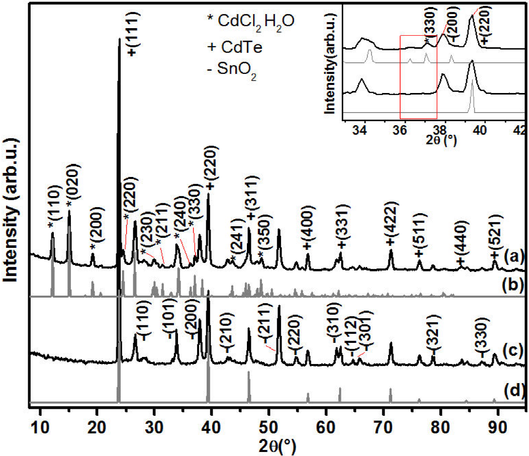
Figure 2. XRD of structures (a) CdTe/TTCdCl2 (TT1), (b) hydrated-CdCl2 modelling, (c) CdTe (TT0) and (d) CdTe modelling.
In the same way a pattern of TT3 was obtained in order to review any changes that could be present on the sample when it is summited under a heat treatment in air and cleaned with distilled water, thus, the Fig. 3a shows how the principal hydrated-CdCl2 peaks was diminished. Is possible that the peaks were eliminated or the percentage present in the sample is less than 5%, if it is the case, we know that X-ray diffraction cannot detect a signal from the compound. In the pattern, the plane (111) reveals that recrystallization occurs when grains belonging to another plane nucleate and grow to reach high fractions of volume and consequently modify the preferential orientation. Doing a quick calculus, we can conclude that the lattice parameter values did not change with the thermal treatment (a = 6.497 Å); respect of FWHM related with the (111) plane values of 0.37° and 0.35° for as deposited CdTe and CdTe (TT3) respectively. Due to the last results the CdTe recrystallization were associated by the intensity variation related with the (111), (220) and (311) planes.

3.2. Morphological properties
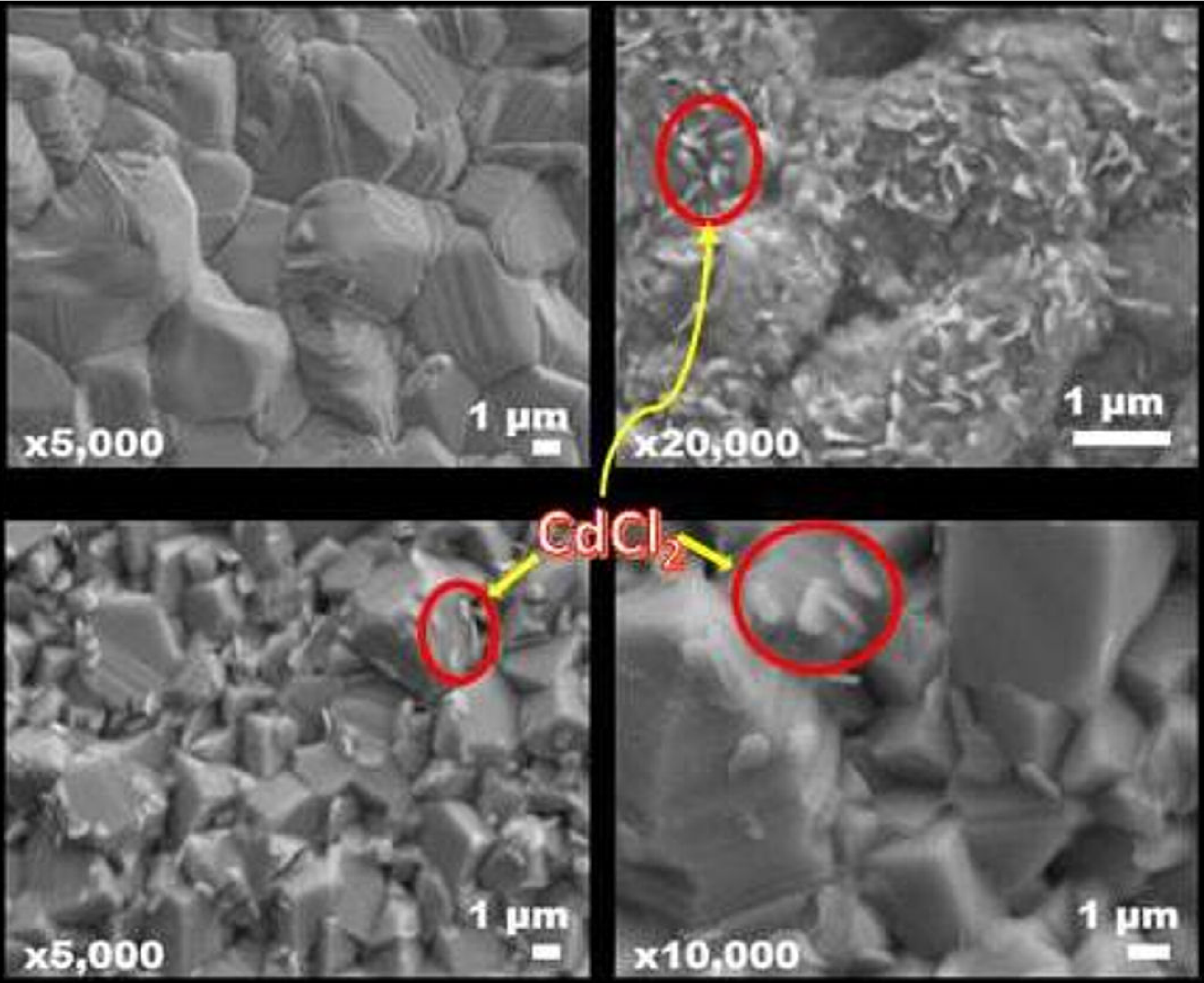
Figure 4a shows a common CdTe morphology growth by CSVT, the samples have a big density of grain boundaries on different faces directions. Considering this observation is necessary implement a treatment in favor of reduce boundaries and increase the carriers flow through the metal contact. As mentioned in the introduction, many works has been developed trying to improve this junction (semiconductor/metal), in this case is possible to see in the Fig. 4b the hydrated-CdCl2 morphology on CdTe surface creating a hydrated-CdCl2 shell, however, this cover allows to see the CdTe boundaries, after hydrated-CdCl2 deposition the sample was heat treatment on air reducing the hydrated-CdCl2 density, therefore, is appreciated a change in the CdTe grains due to the defects on the CdTe surface was reduced and as we could see in X-ray diffraction the CdTe planes are oriented in the (111) direction. Additionally a density of CdCl2 flakes appear on the CdTe surface (see Fig. 4c), this morphology could reduce the current because the boundaries act like recombination centers. In this way a cleaned process was developed using distilled water, and how the Fig. 4d shows the hydrated-CdCl2 flakes density was reduced, obtaining a CdTe recrystallization on (111) direction.
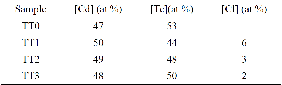
An elemental analysis was done by using EDS, the Table II shows the atomic percentage of Cd, Te and Cl elements present in the different steps of the treatment. In TT0 the Te percentage is more than Cd, this result does not correspond with different authors due to it mentions that CdTe growth by sublimation technique create a rich Cd region, however, for this work the thermal treatment help to create a Te rich region on CdTe surface (TT3 step), Cl signal on the surface decreases considering each step of the process.
3.3. Electrical properties
The hydrated-CdCl2 process was analyzed from electrical point of view to understand what is the behavior of this process on the CdTe surface. Is important to notice that CdTe thin films has a high resistivity (around 3.3 × 10⁵
3.4. Optical properties
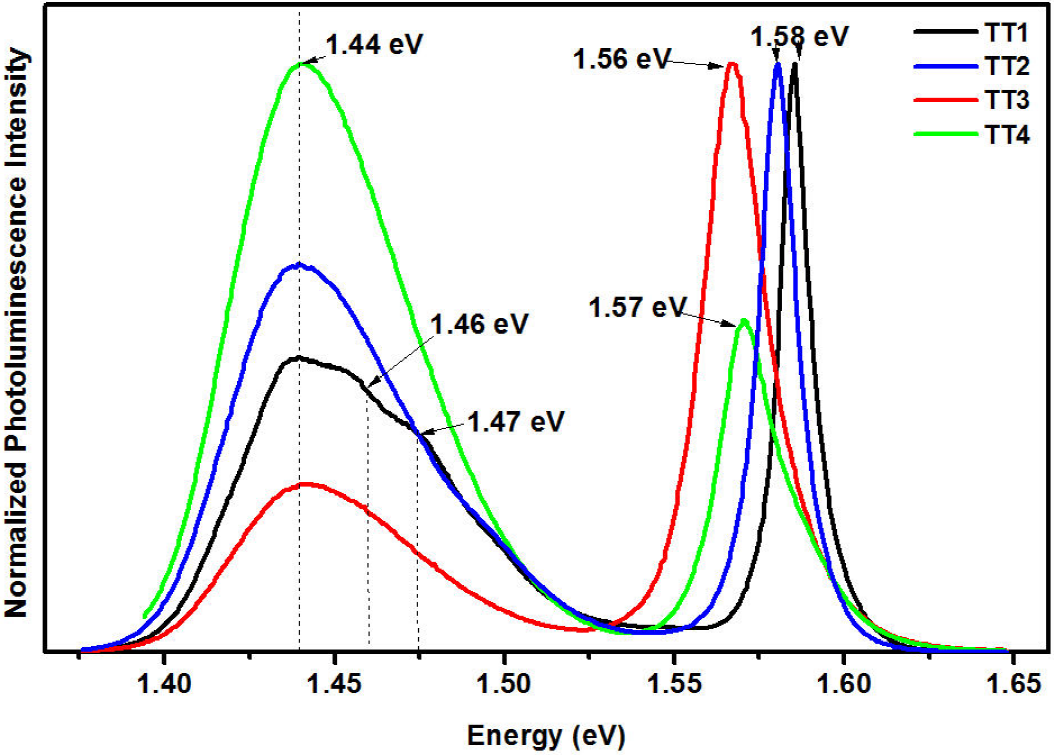
Two principal luminescence bands were observed in the four steps of treatment as shown in Fig. 5. The one present in the range 1.56 eV - 1.58 eV results from donor or acceptor bound excitons. However this shift of the peaks could be produce by OTe acceptors 9 or VCd complex based acceptors participating in a donor-acceptor pair (DAP) recombination. A further band at 1.44 eV is characteristic of a further complex DAP emission often seen in CdTe. There were some important differences between the spectra of the samples. The hydrated-CdCl2 treatment causes a general increase in luminescent intensity indicating either an increase in the concentration of the active centers or a decrease in the non-radiative recombination sites. Considering the CdTe and CdTe treated with hydrated-CdCl2 samples the 1.44 eV band is most intense in the bulk of the CdTe layer after complete treatment, this result origin that DAP luminescence is known to be complicated and possible assignments such as (VCd) as the acceptor and Cl Te as the donor are speculative. Also analysing the PL spectra from CdTe as grown, is possible to identify three bands 1.44, 1.46, 1.47 (eV), who are related to Te deficiency, O presence and donor-acceptor recombination due to ClTe respectively. However, in order to review this last SIMS measurement was done.
A solar cell structure (SC2) was analyzed, four signal of each element present in the solar cell (Cd, Te, S, Cl) are studied in order to see the behavior of Cl into the solar cell. Figure 6a shows the Cl signal in the CdS region, it is present in this part due to the CdS growth considering that involves Cl precursors in addition the front contact also contribute Cl because this film is chemical treated on HCl as part of the process. On another hand, the Fig. 6b shows a different Cl signal behavior, as result of hydrated-CdCl2 process, the CdTe grains recrystallize on (111) plane and a migration of Cl along CdTe structure was determined. As different authors mention the possible Cl migration in CdTe is assured by SIMS, however, is necessary to do another analysis in the interest of determine in which position is localized.

4. Conclusions
Hydrated-CdCl2 was implemented by CSVT on CdTe thin films in order to recrystallize the CdTe surface. XRD confirms the recrystallization in the (111) plane, this was observed in the SEM images and some hydrated-CdCl2 crystals are present on the CdTe surface. The hydrated-CdCl2 treatment causes a general increase in luminescent intensity indicating either an increase in the concentration of the active centers or a decrease in the non-radiative recombination sites. Cl atoms were detected along the CdTe solar cells structures promoting the formation of different compounds in the junctions of the solar cell. The activation leads to modifications in the electronic properties of every layer and interface in the CdTe solar cell.

