


 nueva página del texto (beta)
 Inglés (pdf)
 Artículo en XML
 Referencias del artículo
 Enviar artículo por email
 Citado por SciELO
  Similares en
SciELO
Similares en
SciELO 
 Permalink
1. Introduction
The typical efficiency limit - the so-called “Shockley-Queisser Limit” - is a maximum value, which for many years has been a landmark for solar cells efficiency among researchers, but now it seems that it may be overcome using nanotechnology. Nanotechnology incorporation into the solar cells shows special promise to both enhance efficiency and lower total cost. Nano-structured layers in thin film solar cells offer important advantages, including the energy band gap of various layers that can be tailored to the desired design value by incorporating quantum nanostructures.
In the nanotechnology frame, the race for ultra-high-efficiency photovoltaic cells takes into account quantum well and superlattice solar cells. These approaches consist on the insertion of a multiple quantum well or superlattice system in the intrinsic region of a p-i-n cell of wider bandgap (barrier or host) semiconductor in order to improve the spectral response of the cell in the energy region below the absorption edge of host material. In simple terms, the multiple quantum wells solar cell (MQWSC) and superlattice solar cell (SLSC) are p-i-n structures with sandwiched very thin layers (quantum wells) in the intrinsic layer between the two n and p doped bulk semiconductors. This idea was pioneered by Barnham et al. in 19901. In a MQWSC, the different quantum wells are independent and there is no coupling between neighboring quantum wells. However, for the superlattice solar cell, there is an interaction between neighboring wells and the wave function becomes extended over the whole superlattice, and the discrete levels in isolated quantum wells spread into a miniband. A common feature of these new approaches is that they rely on quantum-based devices for their implementation. Hence, the inclusion of quantum effects in the calculation of solar cell parameters is of increasing importance. The quantized energy levels in quantum structures become the driving force for this kind of next generation solar cells by means of allowing control of the band structure and hence the absorption profile.
For the superlattice solar cell, there is an interaction between neighboring wells and the wave function becomes extended over the whole superlattice, and the discrete levels in isolated quantum wells spread into a miniband. From the theoretical point of view, the advantages of an SLSC over an MQWSC are the following: (i) provides quantum levels for electrons and holes within specific eigen-energies (minibands), (ii) enhances the miniband absorption by increasing available states, (iii) carriers can efficiently tunnel along the growth direction through thin barriers, (iv) allows an efficient escape rate of carriers out of quantum wells for collection in emitter and base regions2.
In presence of electric field (E-field) across the intrinsic region, perpendicular to the layers, the superlattice minibands split into a band energy ladder and as the 𝐸-field is increased, considering wells of equal width with a single energy level; an alignment between the energy subbands is getting worse. On the other hand, when wells have more than a single quantum energy level, it is expected that the bands move in and out of alignment as the 𝐸-field is varied. This effect leads to a variation with field of tunneling probability, and a decrease of the solar cell performance if miniband alignement is not optimally matched to the incident light power (which determines the optimum operating voltage). If the bands are poorly aligned, the 𝐸-field causes a localization of the electron in the quantum well and a vanishing miniband, such that the superlattice advantages disappear. Therefore, the major challenge in the design of this device is to achieve the conditions for resonant tunneling for a specific value of the 𝐸-field which allow the escape of the carrier from the superlattice3.
A proposal to overcome this difficulty is the fabrication of a variable spaced superlattice where a well width variation is chosen so that the electron levels are resonant at the operating bias4,5. However, this superlattice should be fabricated so that the resonance occurs at a particular value of the E-field, which matches with internal field value in the intrinsic region. Thus, SL growing conditions are highly dependent on the doping in the n and p regions, as well as of the intrinsic region width.
The dilute nitride (GaIn)(NAs) is a novel material system grown lattice matched to GaAs. It has been challenging to introduce the most optimal species of nitrogen into the film without creating electronic defects that serve as efficient non radiative recombination centers. A dilute nitride process using molecular beam epitaxy that incorporates antimony as a surfactant has developed junctions. This process enables growth of dilute nitrides films and reduces many of the deleterious effects, such as segregated films, the formation of clusters and interstitial defects, for creating high performance junctions for incorporation into solar cells6. The band gap of GaAs decreases rapidly with the addition of small atomic fractions of 𝑁 7, moreover, the addition of In to GaNAs does not only provide a closer lattice match to GaAs, but also decreases the band gap. This property makes very attractive the use of GaInNAs materials to fabricate superlattice to improve the GaAs solar cell conversion efficiency.
In this paper, a Ga 1−𝑥 In 𝑥 N 𝑦 As 1−𝑦 Gaussian Superlattice (GSL) is incorporated into the intrinsic region of conventional GaAs p-i-n solar cell. We have used GSL because, as it will be shown later, the resonance conditions are less dependent on 𝐸-field variation. This effect is quite different from other SLs, where the tunneling probability has sizable oscillations in each miniband when 𝐸-field changes. Also, the GSL has the outstanding characteristic that the transmission spectrum presents transparency bands or passbands with almost perfect transmission, separated by gaps or stopbands where practically there is not transmission at all. This Gaussian arrangement increases electrons escape probability from the superlattice8. Moreover, GSL presents some plateaus in the transmission characteristic where electrons are almost unscattered9,10.
The width of barriers is modulated by a Gaussian function centered in the middle of the superlattice (𝑍= 𝐿 𝑆𝐿 /2). The height of the barriers was fixed as well as the bottom of the wells by a proper choice of the In and N fractions. The number of GaAs lattice constant of the barrier centered in 𝑍 𝑏 is the integer closest to
where 𝐿 𝑆𝐿 is the superlattice width, 𝑁 max is the number of monolayers at 𝐿 𝑆𝐿 /2, and 𝜎 was fixed to 14 GaAs lattice constants.
To research the GaAs/GaInNAs GSL solar cell (GSLSC), which is schematized in Fig. 1, arrangements with clusters
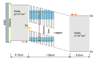
Figure 1 Sketch of energy band diagram of the GSLSC. Gaussian superlattices are embedded within the depletion zone of the GaAs p-i-n solar cell and extends the absorption edge of the cell beyond that of a classical GaAs solar cell. A 40 nm Al0:8Ga0:2As window layer was incorporated into the p-region to reduce front surface recombination and a MgF:SiN layer as antireflection coating was used.
of GSL were optimized to enhance the resonant tunneling between adjacent wells. These GSL clusters are composed by quantum wells of 1% nitrogen composition and 5 GaAs lattice constants of width, parameters where the maximum values of efficiency are obtained11. A series of clusters are inserted in the i-region, independent from each other, in such a way that there is no coupling between neighboring clusters. Also, the 𝑥=2.85𝑦 condition was satisfied such that Ga 1−𝑥 In 𝑥 N 𝑦 As 1−𝑦 is lattice matched to GaAs. GaInNAs parameters were taken from reference12.
In this paper, we establish criteria to calculate miniband widths in superlattice heterostructures in the presence of 𝐸-field through comparative studies of recombination processes, density of states in the direction for the GSL and tunneling probability. Also, a method for optimizing miniband width is presented that could allow significant enhancement of conversion efficiency over the single band gap limit. Similarly, the optical transitions in GSL are evaluated to calculate the quantum efficiency, dark current and the photocurrent, and then they are compared with experimental data. GaAs/GaInNAs GSL solar cell is optimized to reach the maximum performance by evaluating the current-voltage curves under illumination and thus to determine the highest efficiencies for solar cells containing GSL clusters.
2. Miniband width calculation
A simple Kronig-Penney potential model is widely used to calculate miniband widths in superlattice heterostructures, which describes the bound electron states of an infinite periodic potential13,14. The experimental and calculated results match when the Kronig Penney model is used at zero 𝐸-field. However, in presence of an applied 𝐸-field the calculated miniband width disagrees from the experimental width. The localization of the electron in the quantum well by 𝐸-field reduces tunneling current, causing an increase of recombination process. Electronic states with lower energy in SL are more confined leading to increased recombination rate values. Then, these electronic states do not contribute to the formation of a miniband with high tunneling probability values.
We have carried out comparative studies of the recombination processes and tunneling probability to determine more precisely the GSL miniband width in the presence of 𝐸-field. We used the well-known Transfer Matrix Method (TMM) without back-scattered wave approximation to study transmission properties. When the energy of incident particle coincides with energy of quasi-bond state in the well, the tunneling probability value is increased, showing that the resonant tunneling conditions are established in energy minibands for a particular value of the 𝐸-field.
For recombination processes, we have computed the radiative recombination rates by ab-initio methods15. First, we calculated the absorption coefficient using a quantum-mechanical model where the energy miniband is decomposed as a set of discrete energy levels. In the presence of an 𝐸-field, band bending lifts the energy degeneracies that produce the superlattice minibands and the energy spectrum of a superlattice becomes an energy Stark ladder of discrete levels. Transitions between the levels lead to recombination or absorption processes. The discrete energy levels were computed through the peaks in the density of states spectrum in the confinement direction. With these values and assuming a parabolic band structure for electrons and holes in the GSL, the absorption coefficient was calculated using Fermi’s golden rule and the quasi-Fermi-level separation 𝛥 𝐸 𝑓 values for the AM1.5 solar spectrum16
The radiative recombination rate 𝑅 𝑟𝑎𝑡𝑒 depends on the occupation probability functions for electrons, 𝑓 𝑒 , and holes, 𝑓 ℎ , with the same 𝑘-value. At the same time, the occupation probability function for electrons and holes depends on the corresponding quasi-Fermi level. To evaluate 𝑅 𝑟𝑎𝑡𝑒 , we have assumed that the number of photogenerated carrier pairs is equal to the total emitted photo flux.
The 𝑅 𝑟𝑎𝑡𝑒 𝑛𝑗 expression for electrons in the 𝑛 𝑡ℎ -subband is obtained by integration over all possible electronic states:
The integral over 𝑑(ℏ𝜔) is to find the rate for all recombined electron and the integration over 𝑑 2 𝐾 is to get the rate for all the occupied electron and hole subband states.
Equation (2) summarizes the discrete energy states of the electrons (index 𝑛) in the conduction miniband (index 𝑙) and the heavy and light holes (index𝑚) in the valence miniband (index 𝑙′) in the superlattice. 𝐸 𝑛,𝑙 𝑒 ( 𝑘 ) and 𝐸 𝑚,𝑙′ ℎ ( 𝑘 ) denote the GSL subbands of the electrons and holes and 𝛿 denotes the Dirac delta function. The factor 𝐴=2 𝑞 2 𝑛 𝑟 /( 𝑚 0 2 𝑐 3 ℏ 2 ) is a material dependent constant, where ℏ is the reduced Planck constant, 𝑛 𝑟 is the refractive index of the well material, 𝑚 0 is the free electron mass, 𝑞 is the electron charge and 𝑐 is the speed of light. The first term inside the element | 𝑎 ⋅ 𝑝 𝑖𝑓 | represents the polarization unit vector, 𝑎 , while the second term represents the momentum matrix element, 𝑝 𝑖𝑓 . The recombination rate of the SL 𝑠 was calculated using the above formula.
In a semiconductor in nonequilibrium condition, the total electron concentration 𝑛 and the total hole concentration 𝑝 are described to be the electron and hole quasi-Fermi levels, respectively. Applying detailed balance, then each photon produces one electron-hole pair and all recombination events produce one photon, the electrons and hole quasi-Fermi levels in the superlattice structure were calculated following the procedure reported in Ref. 15. A brief procedure description is included for better understanding.
The quasi-Fermi levels are determinate by solving the following system of equations:
where 𝐸 𝐹 𝑒 and 𝐸 𝐹 ℎ are the electron and hole quasi-Fermi levels, respectively.
At low enough carrier density, where 𝛥 𝐸 𝑓 is much smaller than the effective band gap, the Boltzmann approximation is used. Then, the dependency on 𝛥 𝐸 𝑓 is an explicit function given by
where 𝐺 is the gain, which is defined as the number of photogenerated carrier pairs per unit area and time and, it is obtained integrating over wavelength (𝜆) and the superlattice length ( 𝐿 𝑆𝐿 ), the electron-hole pair generation rate at a 𝑧 depth from the surface in the grown direction:
where 𝑅(𝜆) is the surface reflectivity spectrum of the antireflection layer (ARC), 𝛷(𝜆) is the AM1.5 solar spectrum and 𝛼(𝜆,𝑧) is the absorption coefficient to a 𝑧 depth from the surface. The exponential factor is due to the attenuation of light in the layers between the surface of the cell and the depletion layer. The layers considered are antireflection layer, emitter layer, and space-charge region from to the emitter layer (see Fig. 1).
The total electron concentration is calculated by:
where 𝐸 𝑤 𝑒 and 𝐸 𝑤 𝑏 are the conduction band edge energy for quantum well and barrier material respectively, 𝑔 𝑒 𝑆𝐿 (𝐸) is the electron superlattice density of states and 𝑔 𝑒 𝐵𝑢𝑙𝑘 (𝐸) is the electron bulk density of states in the quantum well material. To calculate the total hole concentration we proceed in a similar way. Then the equation system (3) may be solved and the quasi-Fermi levels are determined. The recombination rate between an electron subband and all hole subbands was computed according to Eq. (2).
In Fig. 2, radiative recombination rates and tunneling probability are plotted as a function of energy for a 10 QW GSL under 12 kV/cm transverse 𝐸-field. This value of the built-in field was evaluated taking into account the uniform doping levels, 𝑝 and 𝑛-regions, and intrinsic region width, which are displayed in Fig. 1. This figure also shows the calculated density of states in the direction for the GSL, d 𝑒 𝑧 (𝐸). The 𝐝 𝑒 𝑧 (𝐸) was calculated taking into account applied transversal E-field by the expression17
Where 𝐴 ⊥ is the wave function coefficient in the first region, 𝑆 𝑒11 (𝐸) and 𝑆 𝑒12 (𝐸) are matrix elements in an energy dependent 2×2 transfer matrix for electrons which connects the coefficients of the wave functions at extremes of the heterostructure. Where 𝑙 𝑏 𝑒 =( ℏ 2 /2𝑞 𝑚 𝑏 𝑒 ) 1/3 , 𝜔 𝑏 𝑒 =( 𝑞 2 𝐹 2 /2ℏ 𝑚 𝑏 𝑒 ) 1/3 , where 𝑚 𝑏 𝑒 is the electron effective mass in the barrier and 𝐹 is an applied transverse 𝐸-field. A similar expression for heavy holes and light holes is used. The 𝐝 𝑒 𝑒 spectrum peaks are identified as discrete energy levels for electrons in GSL heterostructure.
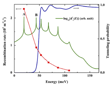
Figure 2 Modeled density of states in the confinement direction, tunneling probability and recombination rates for electrons versus energy for a 10 QW GSL under 12 kV/cm transverse E-field.
As shown in Fig. 2, energy position of A and B peaks are out of the energy miniband where the highest tunneling probabilities are reached. Note that both electron energy levels display the highest 𝑅 rate values. Thus, the 𝐸-field causes a localization of the both electron states in the GSL generating an increase of recombination.
From above mentioned results, we have established the GSL miniband width, for electrons and holes, through the tunneling probability band rather than by the energy separation between the upper and lower energy level of the density of states spectrum.
3. Guidelines to optimize miniband width
In order to achieve higher SLSC performance, it is necessary to increase miniband width, which depends on 𝐸-field, the quantum well number and barrier width. Simultaneously, 𝐸-field depends on doping levels, 𝑝 and 𝑛-regions, and intrinsic region width. For these reasons, it is necessary to optimize the configurations of the GSL structures. By optimizing miniband width, significant enhances of conversion efficiencies over single band gap limit should be achievable.
The miniband width was determined by tunneling probability spectrum. The energy range, where tunneling probability reaches values greater than 0.9, was taken as miniband width. The optimization goal is to improve the spectral response of the cell in the energy region below the absorption edge of host material. In order to gain an extra photon absorption and therefore an increase the short-circuit current; the miniband width must be as large as possible. The GSL resonance conditions are changed when quantum well number and the 𝐸-field are modified. Then, TMM is used to compute the tunneling probability as a function of quantum well numbers ( 𝑁 𝑊 ) and E-field.
The dependence of electron miniband width on 𝑁 𝑊 and 𝐸-field for each cluster is examined in Fig. 3. The quantum well number was varied up to 20 QWs and the 𝐸-field was modified in the range from 1 to 20 kV/cm during the calculation process of the contour plot. Increasing 𝑁 𝑊 , more discrete levels in isolated quantum wells are spread into the miniband because of the interaction between neighboring wells and the wave function becomes extended over the whole GSL structure. In presence of 𝐸-field, the GSL miniband is split into a band energy ladder. With increasing 𝐸-field, the nearest-neighbor coupling is gradually suppressed and the states experience a localization leading a decrease of miniband width. The location effect is clearer with increasing 𝑁 𝑊 , as it is displayed in Fig. 3. A balance between these two phenomena, localization and spread effects, may be found, leading to an optimum number of wells and 𝐸-field for a given GSL. The maximum value of the electron miniband width, 117 meV, is achieved for 12 kV/cm and a 10 QWs cluster, which is shown as black dot in Fig. 3.
Figure 3 also displays that for 10 quantum wells the 𝐸-field can range from 6 to 20 kV/cm and the miniband width remains unchanged. This proves that for GSL the resonance
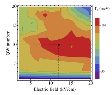
Figure 3 Contour plot of electron miniband width for GaAs/GaInNAs GSL as a function of the quantum well number and the E-field. A maximum value of 117 meV is achieved (black dot).
conditions are less dependent on 𝐸-field variation. Thus, with the minibands in this GSL structure, a significant improvement in optical absorption could be achieved. These minibands also enhance transport of carriers via tunneling through thin potential barriers, hence electrons and holes tunnel to 𝑛-GaAs and 𝑝-GaAs regions, respectively.
4. Photocurrent calculation
Using the same procedures in our previous papers4,15,18, the photocurrent 𝐽 𝑃𝐻 was calculated from the total quantum efficiency of the cell.
In the presence of an 𝐸-field, the energy spectrum of a superlattice becomes a ladder of discrete levels, therefore, it was necessary to extend the procedure reported by Bastard19. Then, we calculate the absorption coefficient for a GSL under 𝐸-field within the envelope function approximation:
where
and
are sums over GSL states 𝑛,𝑙 and 𝑚,𝑙′ which numbers depend on the quantum wells width and depth, 𝛼 𝑒 𝑛,𝑙 −ℎ ℎ 𝑚,𝑗′ (𝐸) and 𝛼 𝑒 𝑛,𝑙 −𝑙 ℎ 𝑚,𝑙′ (𝐸) are the absorption coefficients due to electron-heavy hole and electron-light hole transitions to conduction band, respectively, which considered the exciton absorption. The absorption coefficient due to electron heavy hole transitions 𝛼 𝑒 𝑛,𝑙 −ℎ ℎ 𝑚,𝑗′ (𝐸) was computed by Fermi’s Golden rule:
The formula summarizes the discrete energy states of the electrons (index 𝑛,𝑙) and the heavy holes (index 𝑚,𝑙′) in the GSL. 𝐸 𝑒 𝑛,𝑙 = 𝐸 𝑒 𝑛,𝑗 ( 𝑘 =0) and 𝐸 ℎ ℎ 𝑚,𝑗′ ( 𝑘 =0), 𝐸 𝑒 𝑛,𝑗 ,ℎ ℎ 𝑚,𝑙′ 𝐵 denotes the exciton binding energy and 𝛩(𝐸) is the step function. For the simulation model, the ??-distribution was modified by a Gaussian broadening term to represent the inhomogeneous broadening caused by thermal effects, as well as the deviation from ideality of the QW material properties due to the limitations of the growth. The factor 𝐵=𝜋 𝑞 2 /( 𝑛 𝑟 𝑐 𝑚 0 ℏ) is a material dependent constant and 𝐸 𝑝 is the Kane matrix element (∼23 eV). The first term inside square bracket represents the occupation probability and determines the absorption edge of a bound state where 𝑚 𝑒−ℎℎ ∗ is the reduced mass of the 𝑒−ℎℎ system, and the second term the additional absorption peak contributed by the excitons. Here 𝑎 𝑒 𝑛,𝑗 ,ℎ ℎ 𝑚,𝑗′ denotes the effective Bohr radius of the exciton. For 𝑒−𝑙ℎ transition a similar expression is obtained with ℎℎ replaced by 𝑙ℎ and 𝐸 𝑝 by 𝐸 𝑝 /3. The absorption of the GSL was calculated using the above formula. The other parameters have been previously stated. On the other hand, the exciton binding energies and 𝑎 𝑒 𝑛,𝑗 ,ℎ ℎ 𝑚,𝑗′ were analytically evaluated by variational method [20].
The matrix element contains the electron wave function 𝜒 𝑒 𝑛,𝑙 for the 𝑛,𝑙 electron level and the heavy hole wave function 𝜒 ℎ ℎ 𝑚,𝑗′ of the 𝑚,𝑙′ heavy hole level. In presence of 𝐸-field, the miniband quasicontinuous spectrum is replaced by the evenly spaced Wannier-Stark ladder spectrum and the corresponding wave functions are:
where 𝜙 𝑙 (𝑧) is the 𝑙 𝑡ℎ carrier eigenfunction of an isolated quantum well, 𝐽 𝜍 is the Bessel function of integer index 𝜍, 𝛥 𝜈,?? is the nearest-neighbor transfer integral and is the distance from the reference system origin to the 𝜈 𝑡ℎ quantum well.
The modeled quantum efficiencies as a function of wavelength were computed and compared with Metal1744 sample from the Quantum Photovoltaic Group at Imperial College London. This experimental cell is a p-i-n diode with an i-region containing fifty QWs that are 8.5 nm wide of compres-
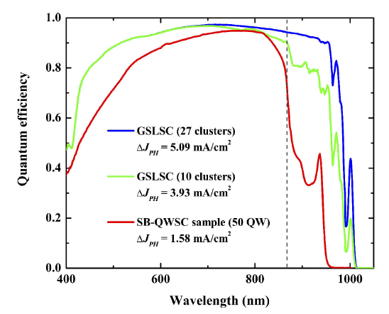
Figure 4 Modelled quantum efficiency versus wavelength for 50 well Metal1744 sample from the Quantum Photovoltaic Group at Imperial College London and 27 and 10 GaAs/GaInNAs GSL clusters.
sively strained In 0.13 Ga 0.87 As inserted into tensile-strained GaAs 0.91 P 0.09 barriers at strain-balance condition. GaAs/GaInNAs solar cells were modeled inserting 27 and 10 clusters of 10 QWs at 12 kV/cm, in the i-region of a GaAs p-i-n solar cell, keeping the device parameters identical as shown in Fig. 1.
Figure 4 displays modeled and experimental quantum efficiencies versus wavelength where it is observed an extra absorption at wavelengths in excess of the GaAs band gap. As consequence of insertion of 10 QWs clusters a notable increase in quantum efficiency above 870 nm is readily apparent, leading increments in the photocurrent which are displayed in Fig. 4. We have used low recombination surface values to model GaAs/GaInNAs solar cells, therefore high quantum efficiency values at short wavelength range are obtained. The modeled GaAs/GaInNAs solar cell exhibits a significant improvement to the spectral response of the cell in the energy region below the GaAs absorption edge, even greater than a strain balance GaAsP/InGaAs/GaAs solar cell, as it is shown in Fig. 4. It is evidenced that the photon absorption by GSL minibands is larger than the photon absorption by multiple quantum wells. Our findings suggest that triple-junction concentrator cells based on a GaAs/GaInNAs bottom cell could reach better performances.
5. J-V relation
We made the common assumptions of homogeneous composition in doped and intrinsic layers, the depletion approximation in the space-charge region, and the total photogenerated carrier collection21. The conventional current-voltage characteristic for a p-i-n solar cell can be written as a function of applied voltage (V) by the well-known Shockley equation for ideal diode, to which the generation and recombination
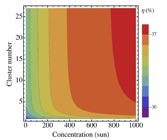
Figure 5 Contour plot of GaAs/GaInNAs GSLSC efficiency as a function of the cluster number and the solar concentration. It shows that it is not possible to increase indefinitely the conversion efficiency by adding more clusters. An increments until 7% of conversion efficiency can be reached from 800 solar concentration.
currents in the intrinsic region of photogenerated carriers are added. Once the expressions for the effective density of states, the absorption coefficient, the radiative recombination current density, and the photocurrent are found for GSLSC, then it is possibly to compute the J-V characteristic, and conversion efficiency (𝜂) can be evaluated18.
The current-voltage relation of the GSL cell is given by:
where 𝑉 is the terminal voltage, ?? 𝐵 𝑇 is the thermal energy, 𝐽 01 is the reverse saturation current density and 𝐽 𝑅1 is the recombination current density. Both current densities took into account the inclusion of quantum wells whose expressions are reported in Ref. 18.
The clusters number in the intrinsic region brings about an opposite effect between photocurrent and the output voltage. By adding more clusters in the intrinsic region the photocurrent is increased but at the same time, the recombination process is enlarged which is necessary to get a balance between generation and recombination. In addition, with the insertion of more clusters in the intrinsic region, the absorption process is increased, moving forward less photons to the deepest layers in the device, originating a drop of the photogenerated carriers in this region. Therefore, the arbitrary incorporation of clusters does not indicate that the photocurrent also would rise, but spreading to saturation as long as the open-circuit voltage ( 𝑉 𝑜𝑐 ) falls due to the increment of the reverse saturation current.
This behavior is shown in Fig. 5, where we have also examined the conversion efficiency as a function of solar concentration for ideal InGaNAs/GaAs GSL solar cells, neglecting resistive effects. Note that at a given solar concentration, the conversion efficiency does not change even if the number of clusters increases because although the photocurrent increases the 𝑉 𝑜𝑐 decreases.
An interesting result is that at 1000x solar concentration, improvements until 7% of conversion efficiency can be reached. Also, this contour plot suggests that with the increment of solar concentration on the device, fewer clusters are required in the i-region in order to achieve high performance.
6. Conclusions
We have presented a new type of photovoltaic device where GSL are inserted in the i-region of a GaAs/GaInNAs p-i-n solar cell. A theoretical model was developed to study the performances of these devices. We have established criteria to calculate miniband widths in superlattice heterostructures in the presence of E-field. It was also shown that optimizing miniband width significantly enhances of the spectral response of the cell in the energy range below the absorption edge of host material were achieved. The cluster number effect on the conversion efficiency was studied showing that for high values of solar concentration, fewer clusters are required in the i-region in order to reach high performance.
Our results indicate that it could be attained better conversion efficiencies that before have never been obtained for a single-gap solar cell. Because of the results that our model predictions are neither compared nor confirmed experimentally, it would be interesting to see if future experiments can corroborate our outcomes.
Solar cell efficiency potential remains far greater than the efficiencies obtained so far, including those achieved in research laboratories. New approaches are necessary in order to increase the conversion efficiency and the GSL GaAs/GaInNAs solar cells could be a road to reach this goal.

