


 nueva página del texto (beta)
 Inglés (pdf)
 Artículo en XML
 Referencias del artículo
 Enviar artículo por email
 Citado por SciELO
  Similares en
SciELO
Similares en
SciELO 
 Permalink
PACS: 81.05.U; 81.05.ug; 81.05.uf
1. Introduction
Diamond films have been proposed for protecting plasma-facing components in tokamak fusion reactors 1. In common with other materials such as graphite, contamination of the plasma and chamber with hydrocarbons and particulates is of concern. Whilst it is known that hydrogen bombardment etches carbon films there is little information about the surface transformation to other carbon structures that may worsen contamination leading to the retention of radioactive isotopes within fusion reactors. In the case of diamond, both theoretical 2 and related experimental studies 3,4,5 have shown that, under particle bombardment, the diamond lattice is converted to a high density thin amorphous carbon layer rather than graphite.
Under chemical vapour deposition (CVD) conditions various carbon structures have been reported, e.g. diamond (nano and poly-crystalline) 6, nanotubes and nanofibres 7, nanospheres 8, nanopipes 9, and micro-trees 10, among others. Experimental conditions to grow different structures vary in temperature (500 to 900°C) 11, pressure (30 to 760 torr), carbon source (methane, acetylene, benzene, ethylene being the most common) 12,13,14,15, and DC bias (150-400 V) 16. We know that fibres as well as nanotubes and other nanostructures 17 are synthesised in catalytic CVD using catalyst particles such as Fe, Ni, Co, Cu or their alloys. Metal thin films have also been used as catalysts: the technique allows the formation of metal nanoparticles after thermal or plasma etching of the film 12,18.
Carbon structures have been produced for applications such as: energy storage 14, catalyst support materials 19,20,21 composite materials 22, selective adsorption agents 23,24, electrodes 25,26,27 and the production of flat panel displays, nano-transistors in computer technology28,29,30,31, among others.
The aim of this work is to study the formation of fibres, sheets and tubes on diamond film substrates during hydrogen etching conditions in the presence of silicon. The diamond films used in this study exhibited different characteristics such as morphology and diamond quality (sp3/sp2 ratio) and the resulting fibres, sheets and tubes growth mechanisms are related to the substrate and hydrogen etching conditions.
2. Experimental
The nanocrystalline diamond films materials, exhibiting different morphology and sp3/sp2 ratio, were deposited by different growth conditions selected from previously reported experiments 32. Diamond film deposition and fibre production were carried out in a 2.45 GHz microwave plasma enhanced CVD reactor described elsewhere 33. The reactor design, for the growth of electronic grade diamond, eliminated the need for a quartz bell jar or other source of silicon near the plasma. Graphite substrates for diamond deposition were 20×20×3 mm3 highly oriented pyrolytic graphite (HOPG) pieces (Ringsdorff Werke GmbH, Bonn, Germany).
Diamond film deposition was achieved under the following conditions. For sample 1, the film was grown on an ultrasonically scratched substrate (Bandelin Sonorex Digital 10P ultrasonic bath, for 30 min) with a suspension of 3% nanodiamond/methanol (detonation nanodiamond was cleaned by the procedure described by Jiang and Xu 34) and CVD deposition was carried out using 1.5 kW input microwave power. Sample 2 was treated as sample 1 but CVD deposition was achieved using 3 kW input microwave power. For sample 3 the film was prepared on an ultrasonically scratched substrate with 3% microdiamond in methanol (1
The gas mixture used in all the experiments was 5% CH4/15% H2/80% Ar with a total gas pressure of 100±2 torr, for 2 hours. For the growth of carbon fibres, sheets and tubes a crystalline silicon (5×5 mm2) wafer was placed on top of the pre-deposited diamond and a hydrogen plasma treatment was carried out for 15 min using 4.2 kW power at 50 ± 2 torr. All substrates were heated by the plasma, without additional heating, and the sample temperature was measured using a two-colour optical pyrometer.
Samples were characterised by scanning electron microscopy (SEM, Hitachi 2700, operated at 10 keV electron energy and with a secondary electron emission detector). Sample 2 was also analysed by SEM at the Electron Microscope Facility, University of St. Andrews, UK (Jeol JSM 5600, operated at 5 keV). Raman spectroscopy (Renishaw Ltd, inVia Raman microscope) used an excitation wavelength of 514.5 nm. The Raman spectra were collected from 1000 to 2000 cm-1 and the data were fitted using Gaussian profiles in OriginLab© Data Analysis. X-Ray Photoelectron Spectroscopy (XPS) measurements, using Mg K
3. Results and Discussion
Hydrogen etching of diamond, under similar experimental conditions to those presented here, reveals steps and pits and removes primarily non-diamond carbonaceous material 35. When a piece of silicon wafer is introduced on top of the samples, the silicon is etched (Fig. 1a) and the growth of fibres, sheets and tubes is seen in the vicinity. Carbon fibres, sheets and tubes were evident on the diamond substrate when silicon was present, through silicon transportation-inducing nucleation sites as observed in nanodiamond films (Fig. 1b).
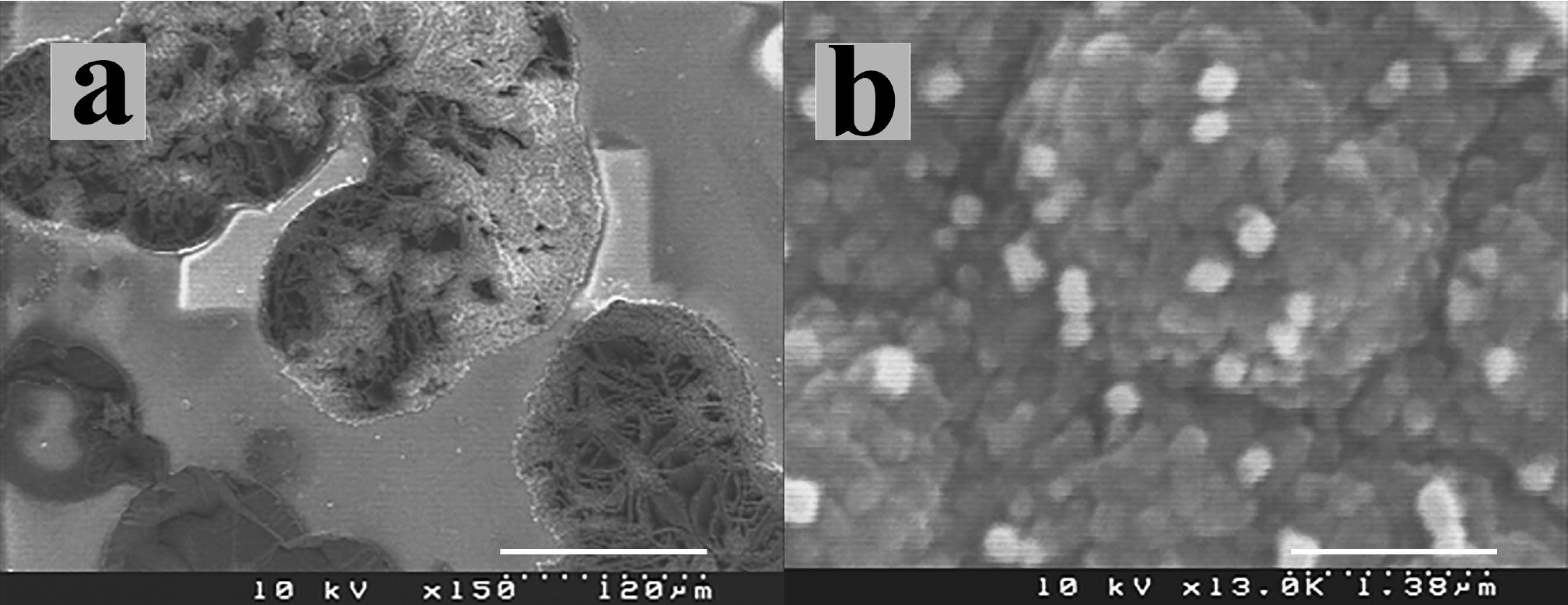
Figure 1. SEM micrographs from (a) etched silicon piece on the top of diamond films during fibre growth, (b) cumuli formation in nanodiamond films.
Fibres grown on diamond films with different sp3/sp2 ratios (determined by deconvolution of the Raman spectra, Table I) present distinct morphologies. Lower quality diamond films (sp3/sp2 ratio) were etched faster, increasing the carbon (primarily in the form of methane) concentration in the plasma, which in turn will influence the ultimate carbon structures.
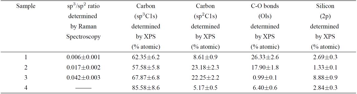
Table I. sp3/sp2 ratio determined by Raman and XPS analyses of the sample surfaces from the areas of the core line spectra (% atomic).
Sample 1 corresponds to thin bent fibres grown on ananodiamond surface with sp3/sp2= 0.006 (Fig. 2a), with an approximate diameter of 360 nm (dimensions estimated by SEM micrographs) as shown in Fig. 2c. A high density of fibres was seen covering the film surface in this sample (Fig. 2b) compared to sample 2, evidently caused by a higher nucleation density. Since the etching of non-diamond material is more facile, a lower film quality will produce a higher carbon level above the surface resulting in a greater nucleation density. Fibres in Sample 2, were grown on a nanodiamond surface with a sp3/sp2 ratio of 0.017 (Fig. 3a). In contrast the resulting fibres were thicker and short (0.5
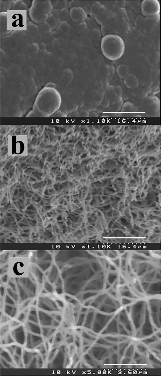
Figure 2. SEM micrographs from sample 1 showing: (a) nanocrystalline diamond film before carbon fibre growth; (b) fibre growth on diamond film, (c) bent and thin carbon fibres.
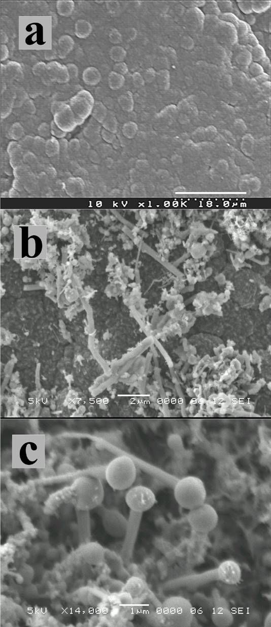
Figure 3. SEM micrographs from sample 2 showing: (a) nanocrystalline film, (b) after hydrogen etching showing fibre growth, (c) short and thick fibres with round tips resembling pins.
Wunderlich 16 proposed that low concentrations of carbon growing species produce thin nanotubes (e.g. single wall carbon nanotubes) that have fast reaction velocity. Multi-wall carbon nanotubes and graphite nanofibres have lower reaction velocities since they have to fill the three-dimensional volume. These features of the mechanism explain the variation of the thickness of fibres seen in samples 1 and 2. Thick and short fibres in sample 2 are the result of low reaction velocities, compared to the thin and long fibres in sample 1.
Sample 3 had sheets producing flower-like shapes (Fig. 4) that grow perpendicular to the diamond film in etched pits (Fig. 4b). Figure 4c shows an etched pit where the removed diamond surface reveals the first stage of diamond growth with rod-like morphology. We believe that carbon sheets grow onto the edges of these rods, and the different orientations of these rods produce the flower-like shape. The diamond quality is higher than samples 1, 2 and 4 and thus the etching rate and nucleation density is much lower. Similar flower-like shapes have been produced by laser ablation 37 and they have been synthesised in solvents under heating-cooling sequences 38,39 but to the best of our knowledge, this is the first time these structures have been observed under CVD conditions.
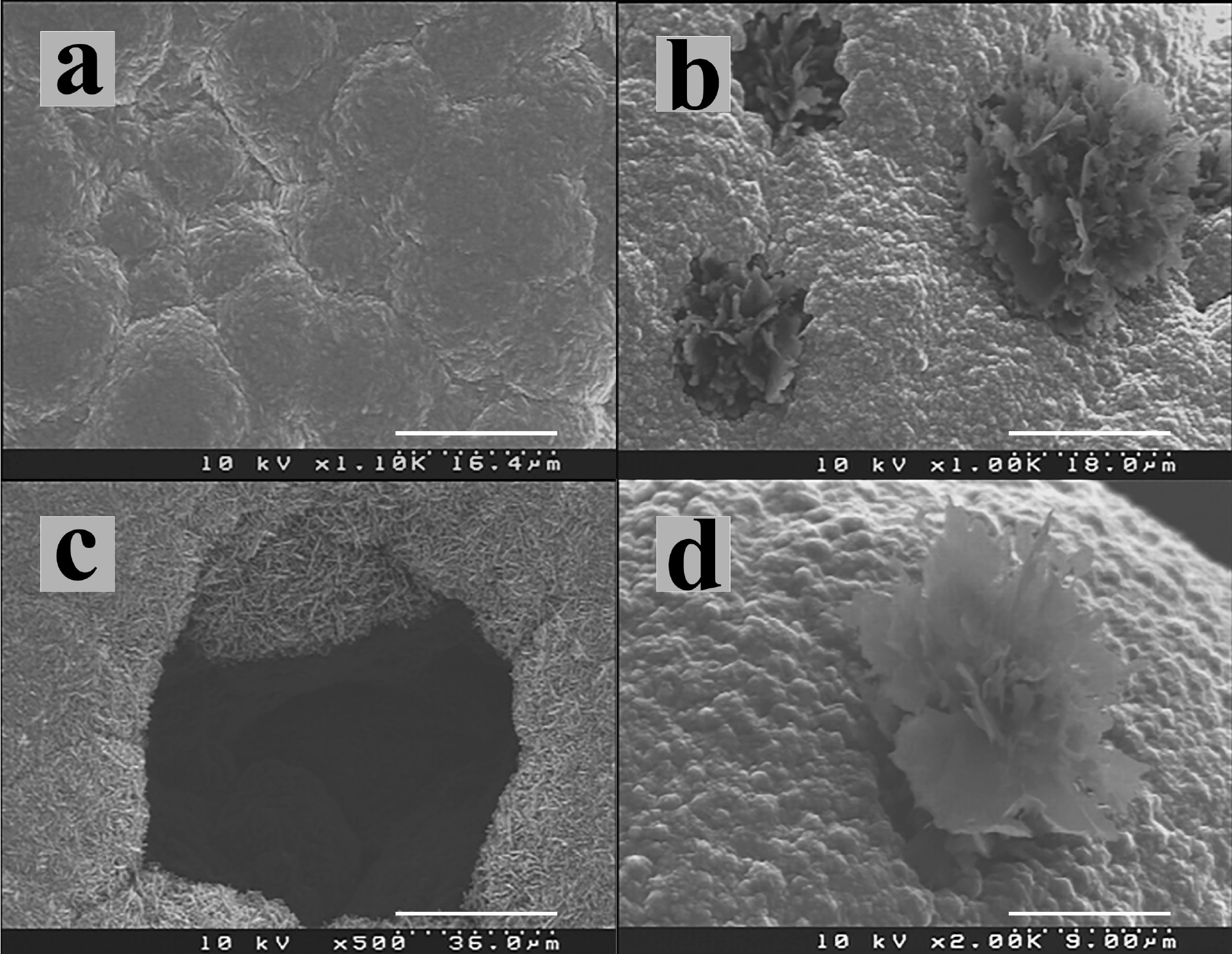
Figure 4. SEM micrographs from sample 3 showing: (a) nanocrystalline diamond film before carbon sheets growth; (b) sheets growth on diamond film, (c) etched pits showing initial growth of rod-like diamond. d) Single flower-like structure.
Figure 5 shows SEM micrographs from sample 4. For the nanocrystalline film shown in Fig. 5a, amorphous carbon growth (Fig. 5b) is evident after hydrogen treatment together with tubes of 600 nm in diameter and 750 nm length (Fig. 5c). It has been reported that the destruction of carbon nanotubes by bombardment occurs, forming conical shaped amorphous carbon layers, similar to the ones presented here 16. We believe that the high etching rate of the film, and rapid deposition of graphitic material produce these amorphous materials.
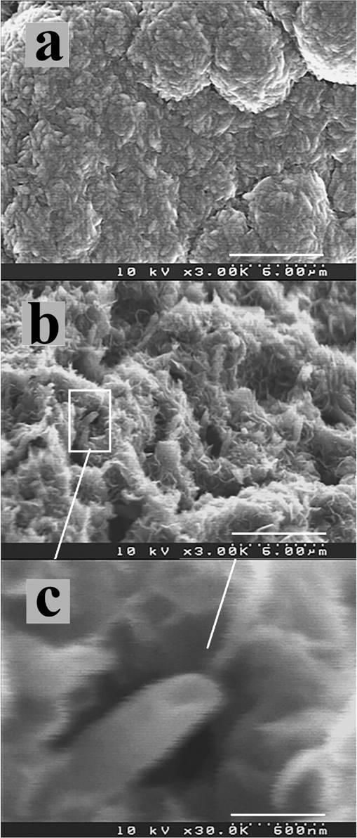
Figure 5. SEM micrographs from sample 4 showing: (a) nanocrystalline diamond film before carbon sheets growth; (b) amorphous carbon with some visible tubes; c) detail of tube.
In Fig. 6 we can see the results from the Raman spectroscopy analysis for all the samples. The spectra present contributions from nanocrystalline diamond or transpolyacetylene at 1135 and 1477 cm-1; this feature has been attributed to the presence of polymeric sp2 species at the grain boundaries 40. The broad D-band at
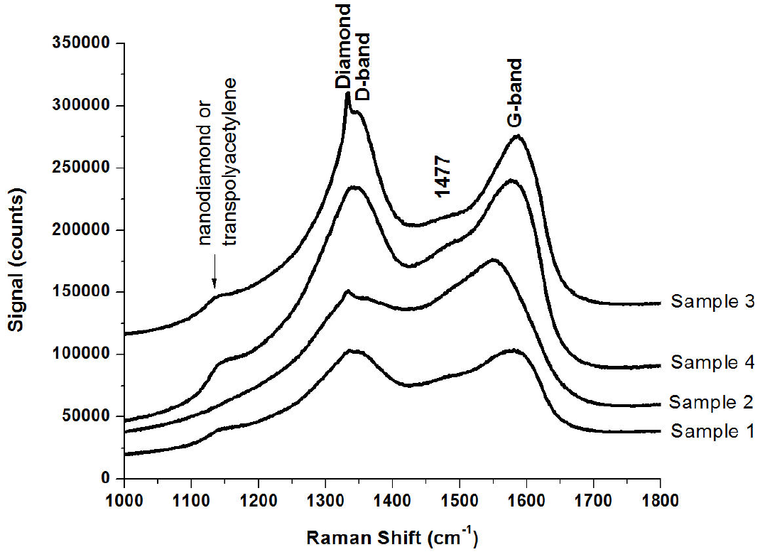
Figure 6. Raman spectra of the prepared samples containing carbon fibres, sheets and tubes grown on nanodiamond films substrates.
The XPS spectra of nanocrystalline and polycrystalline layers (an example is presented in Fig. 7, from sample 1) show an intense and sharp C1s signal at a binding energy of
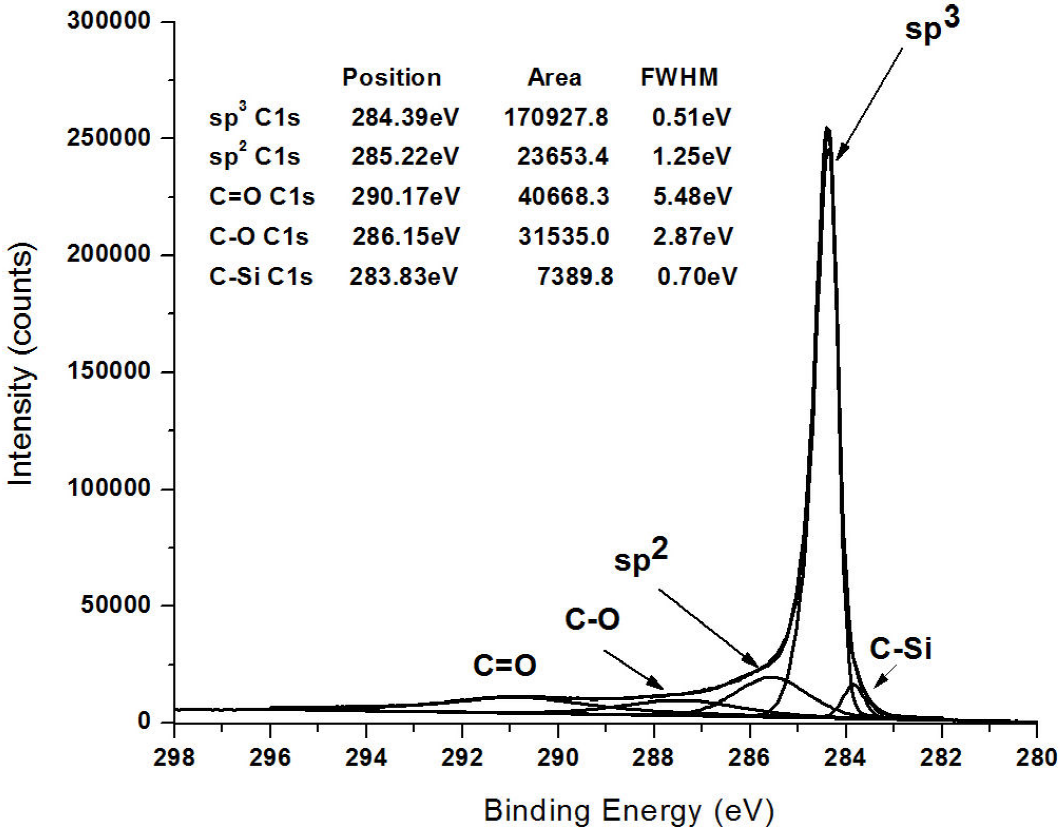
Figure 7. Typical deconvolution of C1s peak of the prepared carbon fibres, the one shown here corresponds to sample 1.
XPS analysis of a pristine graphite substrate showed the presence of 1.2 at% of oxygen (not shown here) which, after diamond deposition, reduces to around 1 at% for all samples. After hydrogen etching, the oxygen content increased in samples 1, 2 and 3 to 26.33 at%, 17.90 at% and 6.40 at% respectively. The presence of peaks from ether and especially carboxylic acid (or ester) functional groups at
4. Conclusions
The production of carbon fibres, sheets and tubes reported in this study provides information on the behaviour of diamond films under hydrogen plasma etching conditions in the presence of silicon. The carbon morphology of the fibres, sheets and tubes depended on the crystalline quality and structure of the diamond film used as a substrate. Silicon plays a key role in fibre production following plasma induce transportation to the fibres during growth. Flower-like shaped carbon structures were also observed following hydrogen plasma etching under different nucleation and plasma conditions than those used in the production of fibre or tubes. The surfaces of the structures were oxygen terminated as, evidenced by the XPS data.
The results of this work open the possibility to other applications such as catalysis, sensors and the production of electrodes, since they combine the unmatchable properties of a diamond supporting substrate with the unique properties of carbon fibres, sheets and tubes. These structures also offer some insight into the variety of formations that may arise from carbon that is hydrogen-plasma etched in the presence of additional elements, such as occurs in tokamak fusion reactor chemistry.

