SciELO - Scientific Electronic Library Online

 
vol.63 número1Design and development of an elastic-scattering lidar for the study of the atmospheric structureSíntesis y caracterización de nanopartículas de paladio, depositadas sobre un soporte modificado de TiO2 y su estudio en la reacción de oxidación de CO a CO2 índice de autoresíndice de assuntospesquisa de artigos
Home Pagelista alfabética de periódicos  

Serviços Personalizados

Journal

Artigo

Indicadores

Links relacionados

  • Não possue artigos similaresSimilares em SciELO

Compartilhar


Revista mexicana de física

versão impressa ISSN 0035-001X

Rev. mex. fis. vol.63 no.1 México Jan./Fev. 2017


Research

Characterization of highly doped Ga0.86 In0.14As0.13Sb0.87 grown by liquid phase epitaxy

J. Díaz-Reyesa  * 

M. Galván-Arellanob 

J.G. Mendoza-Alvarezc 

J.S. Arias-Cerónd 

J.L. Herrera-Péreze 

E. López-Cruzf 

aCentro de Investigación en Biotecnología Aplicada, Instituto Politécnico Nacional, Ex-Hacienda de San Juan Molino Km. 1.5. Tepetitla, Tlaxcala. 90700. México,

bDepartamento de Ingeniería Eléctrica, SEES, Centro de Investigación y de Estudios Avanzados del IPN, Apartado Postal 14-740. Cd. de México, 07000, México.

cDepartamento de Física, Centro de Investigación y de Estudios Avanzados del IPN, Apartado Postal 14-740. Cd. de México, 07000. México.

dCatedrático CONACYT, Departamento de Ingeniería Eléctrica, SEES, Centro de Investigación y de Estudios Avanzados del IPN, Apartado Postal 14-740. Cd. de México, 07000. México.

eUPIITA-IPN. Av. Instituto Politécnico Nacional, 2580, Barrio La Laguna, Ticomán, Cd. de México, 07340. México.

fInstituto de Física “Luís Rivera Terrazas”, Benemérita Universidad Autónoma de Puebla, Apartado Postal J-48, Puebla, Puebla 72570, México.


Abstract

Ga0.86In0.14As0.13Sb0.87 layers lattice-matched to (100) Te-GaSb have been grown using the liquid phase epitaxy technique under supercooling conditions. N and p type layers were grown by adding tellurium or zinc in a wide range of molar fraction in the growth solution. By Raman spectroscopy, the structural quality of the epilayers was characterized. The Raman spectra show that the layers become more defective as the dopant molar fraction is increased, n- or p-type. Two main bands are observed in the Raman spectra centered at 230 and 245 cm-1 that depend strongly on the incorporated dopant molar concentration (Te or Zn), which are assigned to the observed vibrational modes of GaAs-like and (GaSb+InAs)-like mixture. The low-temperature photoluminescence of n (or p)-type GaInAsSb was measured as function of dopant concentration added to the melt solution. The photoluminescence spectra were interpreted taking into account the nonparabolicity of the conduction (or valence) band. Both the band filled as well as band tailing effects due to Coulomb interaction of free carriers with ionized impurities and shrinkage due to exchange interaction between free carriers were considered in order to properly be taken into account for the observed features of the photoluminescence spectra. It is shown that the band-to-band transition energy can be used to estimate the free carrier concentration in GaInAsSb for a wide range of dopant concentration.

Keywords: GaInAsSb semiconductors; Liquid phase epitaxy growth; Photoluminescence spectroscopy; Raman

Resumen

Capas de Ga0.86In0.14As0.13Sb0.87 con coincidencia de parámetros de red a Te-GaSb (100) han sido crecidas mediante la técnica de epitaxia en fase líquida en condiciones de sobre-enfriamiento. Capas tipo n y p fueron crecidas mediante la adición de teluro y zinc en un amplio rango de fracción molar en la solución de crecimiento. Por espectroscopia Raman, se caracterizó la calidad estructural de los epicapas. Los espectros de Raman muestran que las capas se hacen más imperfectas a medida que aumenta la fracción molar de impurificante, tipo-n o -p. Dos bandas principales se observaron en los espectros Raman centradas en 230 y 245 cm-1 que dependen fuertemente de la concentración molar del impurificante (Te o Zn), que son asignados a los modos de vibración observados de GaAs-like y a la mezcla (GaSb + InAs)-like. La fotoluminiscencia a baja temperatura de GaInAsSb tipo-n (o p) se midió como función de la concentración de impurificante añadido a la solución en estado fundido. Los espectros de fotoluminiscencia se interpretaron teniendo en cuenta la no-parabolicidad de la banda de conducción (o de valencia). Tanto el llenado de la banda, así como los efectos de asimetría de la banda debido a la interacción coulombica de portadores libres con impurezas ionizadas y contracción debido a la interacción de intercambio entre portadores libres fueron considerados para tener debidamente en cuenta las características observadas en los espectros de fotoluminiscencia. Se muestra que la energía de transición de banda a banda puede ser usada para estimar la concentración de portadores libres en GaInAsSb para un amplio rango de concentración de impurificante.

Palabras clave: Semiconductores; GaInAsSb crecimiento epitaxial en fase líquida; espectroscopia de fotoluminiscencia; Raman

PACS: 63.20.-e; 64.70.kg; 61.66.Dk; 61.72.sd; 71.20.Nr; 71.55.Eq; 78.30.Fs; 78.55.Cr

1. Introduction

The quaternary alloy system Ga 1-x In x As1-ySb y is of great importance for optoelectronic applications because its room-temperature band gap energy covers the extremely wide range from 1.43 to 0.10 eV. Lattice matched to InP substrates, the band gap energy for the GaInAsSb alloy is nearly fixed, ranging from 0.74 to 0.78 eV. However, lattice matched to GaSb, this band gap energy varies between 0.73 and 0.29 eV, corresponding to a wavelength range from 1.7 to 4.3 μm. This is a very interesting wavelength range for anticipated future fiber optic communication systems. The development of new optical fibers, such as the heavy metal fluoride fibers, offers a possible reduction of one or two orders of magnitude in transmission losses as compared with conventional Si02 fibers; the minimum loss is expected to occur in the wavelength range between 2 to 4 μm1. The alloy system Ga 1-x In x As1-ySb y has received relatively little attention until recently because it is known to have a very large miscibility gap2 with a critical temperature estimated to be 1467°C. As shown by Nakajima et al.3, this restricts the range of solid alloys which can be grown by liquid phase epitaxy (LPE). Dolginov et al.4 reported the LPE growth of alloys near GaSb, with values of x smaller than 0.2 and values of y greater than 0.8. Kobayashi et al.5 and Kano et al.6 have studied the LPE growth of Ga 1-x In x As1-ySb y on GaSb substrates with x limited to the range < 0.18. More recently, DeWinter et al.7 reported the LPE growth of Ga 1-x In x As1-ySb y on GaSb substrates with values of x as large as 0.22; this corresponds to a band gap energy of 0.53 eV (2.33 μm). This is a slight penetration into the predicted miscibility gap (0.18 < x < 0.84)2.

Among many techniques to grow Ga 1-x In x As1-ySb y epitaxial layers on GaSb substrates, Liquid Phase Epitaxy (LPE) still remains an attractive method due to its simplicity and high crystalline quality material it produces. But the existence of a large miscibility gap3 hinders the growth of Ga 1-x In x As1-ySb y in a wide range of x and y values. It is considered a metastable alloy, with the tendency to decompose into regions of non-uniform alloy composition. It should be noted that, owing to the large unstable region, only GaSb-enriched solid solution compositions will be stable at typical LPE temperatures with lattice-matching to GaSb substrates8. This is why trying to reduce the band gap energy of the quaternary antimonide-based material for the desired value for thermophotovoltaic (TPV) applications, usually results in phase separation.

In this paper reports the structural and luminescence properties of Te (or Zn)-doped GaInAsSb with the varying Te (or Zn) molar fraction, using Raman spectroscopy and photoluminescence. After thorough investigation of doped GaInAsSb, we have found a relationship of the main energy emission band versus (Te or Zn) dopant molar fraction added to the growth solution, which could be considered a useful tool to determine the free carrier concentration in doped GaInAsSb by low temperature PL spectra measurement. The carrier concentration increases with increasing dopant mole fraction. In this work we report a systematic study and a quantitative evaluation of the effects of high Te (or Zn) doping in GaInAsSb layers grown on (100) GaSb substrates by liquid phase epitaxy (LPE) using the Raman spectroscopy and photoluminescence (PL) spectroscopy technique.

2. Experimental details

Quaternary GaInAsSb epitaxial layers were grown in a three-zone furnace under H2-atmosphere, using a horizontal graphite sliding boat. As substrates, (100) Te-GaSb wafers mechanically polished from Firebird, Inc. were used. All the precursor elements used to prepare the growth melt were of 6N purity, and the GaAs came from a wafer. For carrying out the intentional doping of the epilayers for high electron (or hole) concentration, Sb2Te3 (or Zn) pellets were added in small amounts to the growth solution. After the charge of the substrate into the boat, the temperature was raised at 640°C for one hour, in order to eliminate the oxides in the substrate surface. Then, the temperature was decreased to stabilize the system, and a cooling ramp at a rate of about 0.3°C/min was established, after which the layers were grown at temperatures of around 530°C. Elemental chemical microanalysis measurements were performed using a scanning electron microscope (SEM) FEI-Quanta 3D FEG model equipped with an X-ray dispersive energy microanalysis system (EDX). Polarized Raman scattering experiments were performed at room temperature in the near-backscattering geometry using the 6328 Å line of a He-Ne laser at normal incidence for excitation. The light was focused to a diameter of 6.0 μm at the sample using a 50x (numerical aperture 0.9) microscope objective. The nominal laser power used in these measurements was 20 mW. Scattered light was analyses using a micro-Raman system (Lambram model of Dilor), a holographic notch filter made by Kaiser Optical System, Inc. (model superNotch-Plus), and a 256 x 1024-pixel CCD used as detector cooled to 140 K using liquid nitrogen, and two interchangeable gratings (600 and 1800 g/mm). Typical spectrum acquisition time was limited to 60 s to minimize the sample heating effects. Photoluminescence measurements were carried out by exciting the sample with the 488 nm line of an Ar+-ion laser, the excitation power was 120 mW and the measuring temperature was 15 K with the sample enclosed in the cold finger of a closed-cycle He cryostat. Sample radiative emission was analyzed through an Acton monochromator and detected with an InSb infrared detector EG&G Judson cooled with liquid nitrogen. Assignation of each transition was accomplished by studying the behavior of the PL spectra with the excitation power. The energy positions and the Full-Width at Half-Maximum (FWHM) of each peak were determined by a quantitative fit to the experimental PL spectra using a sum of Gaussian line distributions; the dominant peaks were fit first and the additional peaks were added as necessary. Ga0.86In0.14As0.13Sb0.87 layers with different tellurium or zinc concentrations were grown by LPE adding small quantities of Te (or Zn) to the growth solution as is indicated in Tables I and II.

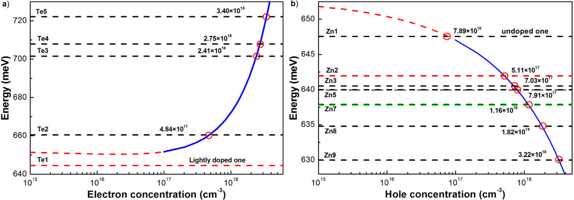
Table I. Summary of the GaInAsSb samples studied, and the Sb2Te3 fraction molar added to each one. All samples were grown at 530°C on single crystal GaSb substrates. 

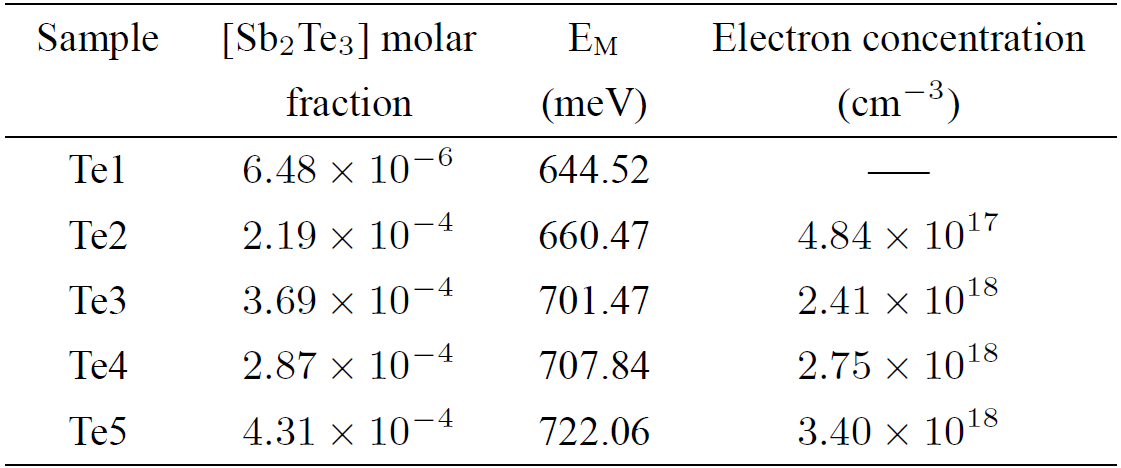
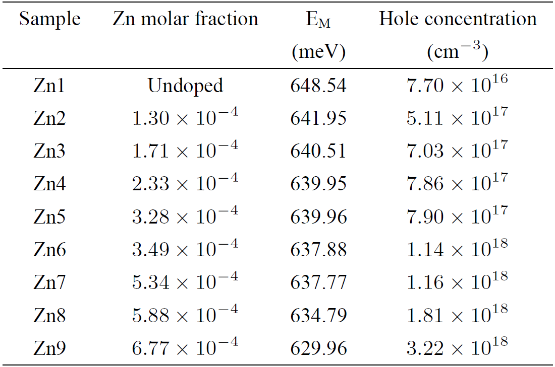
Table II. Summary of the Ga0.86In0.14As0.13Sb0.87 samples studied in this work, which were grown by liquid phase epitaxy and different Zn molar fractions were added to each one. All samples were grown at 530°C on single crystal Te-doped GaSb substrates. The fourth column shows the hole concentrations estimated by low temperature photoluminescence measured at 15 K and at a laser power of 120 mW. 

3. Results and discussion

For all the Te (or Zn)-doped Ga0.86In0.14As0.13Sb0.87 layers, the surface morphology was very smooth, i.e. mirror-like surface without any pinholes, as confirmed by optical microscopy and atomic force microscopy (AFM). The surface morphology was generally very smooth with a root-mean-square (rms) roughness of 19-39 Å as determined from tapping mode AFM.

It is interesting to consider the effect of tellurium as group VI dopant (or of zinc as a group II-dopant) on the structural and optical properties of GaInAsSb solid solutions. It means that Te atoms as substitutional impurity can substitute Sb atom in the GaSb lattice since the covalent radius of Te (a Te=0.136 nm) is nearly the same as that of Sb (a Sb =0.140 nm). Zn is an acceptor impurity in GaSb and its alloys, which means that Zn atoms as substitutional impurities can substitute Ga atoms in the GaSb lattice since the covalent radius of Zn atom (a Zn =0.125 nm) is nearly the same as that of Ga atom (a Ga =0.126 nm). The influence of these dopants on the GaInAsSb physical properties has been studied using the Raman spectroscopy and low-temperature photoluminescence for high doping regime.

The chemical composition of a typical sample was analyzed by EDX. The Zn7 EDX measurement showed the presence of oxygen (0.35%) in the samples along with zinc, indium, antimony, gallium and arsenic. It is widely accepted that oxygen is a residual impurity that introduces deep traps into III-V semiconductor compounds9, which are dominating non-radiative deep centers located below the conduction band that critically reduce the luminescence efficiency9,10. Thus, it appears that oxygen has replaced antimony or arsenic at a few random points of the GaInAsSb lattice. The EDX spectrum indicated that the sample contains a significant amount of carbon (0.78%). From EDX characterization, the chemical stoichiometry of the quaternary layers was deduced for all the samples as approximately: Ga0.86In0.14As0.13Sb0.87.

Back scattering geometry has been used to record the Raman spectra of the GaInAsSb epitaxial layers grown with different tellurium and zinc molar fractions that are shown in Figs. 1 and 2. Raman spectrum of undoped GaInAsSb layer presents four well resolved bands. There are two dominant bands observed at about 227 and 241 cm-1, which were labelled as A and B, and one small band located at 269 cm-1, labelled as C, which does not depend on the tellurium concentration incorporated into the n-type layers. The band C at 269 cm-1 is associated to GaAs TO-like mode11. For the case of p-type layers, the band χ disappears gradually as the zinc concentration is increased in the epitaxial layers indicating that the films have a better crystallinity.

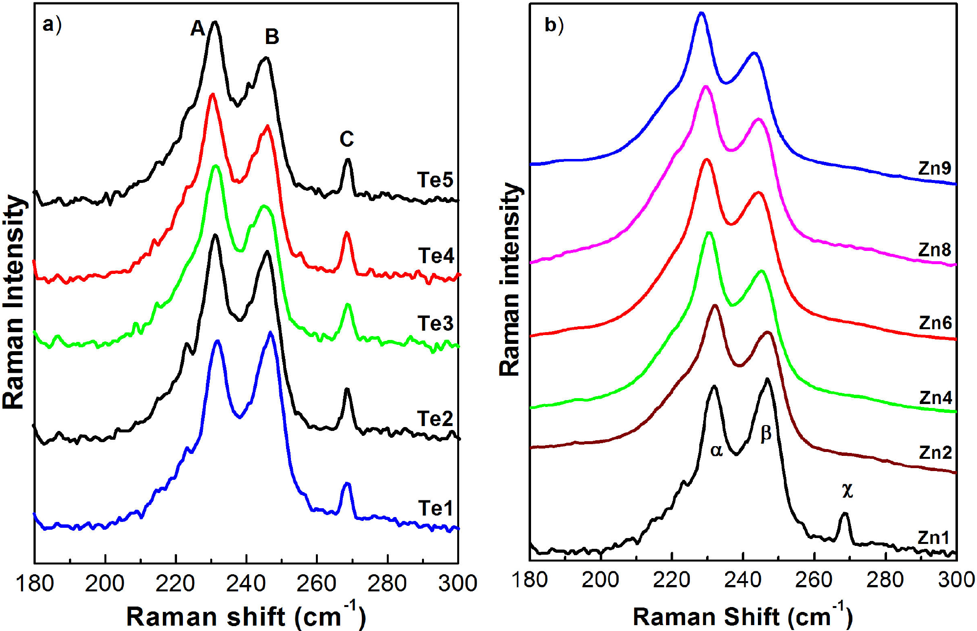
Figure 1. Raman spectra measured at 300 K for the LPE-grown GaInAsSb epitaxial layers with different dopant concentrations: a) tellurium and b) zinc. 

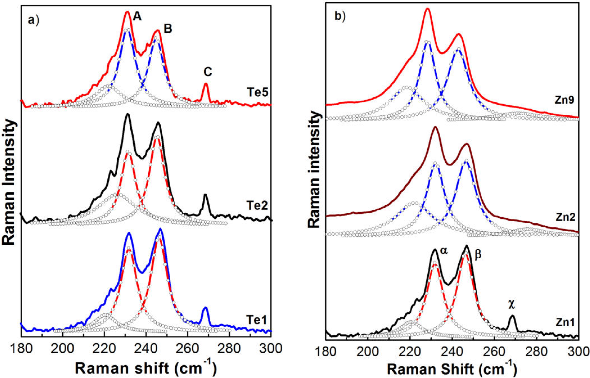
Figure 2  Decomposition of the measured GaInAsSb Raman spectra into individual components (Lorentzian shape) for three carrier concentrations: a) n-type; lightly doped, doped and highly doped. b) p-type: undoped, lightly doped and highly doped. Layers were grown on n-type GaSb substrates. The lines (-o-o-) are their respective fitting. 

The ratio of intensities of the bands A/B ( α/β) increases with the increase of tellurium (zinc) concentration incorporated into the layers; this effect will be explained later. The bands B ( β) and C (χ) can be associated to vibrational modes of the semiconductor binary compounds GaSb, GaAs and InAs12,13. These bands can be deconvoluted in three Lorentzian line shape signals as shown in Fig. 2, which are centered at 246.2, 231.8 and 221.1 cm-1 for the n-type lightly doped (Te1) and undoped (Zn1) samples. In this figure are depicted only Raman spectra corresponding to the samples: n-type; a) undoped, (b) lowest Te-doped (2.19 x 10⁻⁴) and (c) the highest Te-doped (4.31 x 10⁻⁴). For p-type: a) undoped, (b) lowest Zn-doped (1.3 x 10⁻⁴) and (c) the highest Zn-doped (6.78 x 10⁻⁴). The enhanced intensity of the two vibrational modes is due to the fact that the alloys are rich in GaSb and GaAs. The Raman shift of these vibrational modes in the alloys is modified with respect to its bulk values due to the effect of the internal stress originated on the difference in lattice constant between GaSb, InAs and GaAs13 and the incorporation of tellurium (or zinc). Taking into account that phonons are active in the first order Raman process in backscattering configuration on the (001) face, the vibrational bands observed around 216.9, 226.9 and 241.2 cm-1 are assigned to the TO-(GaSb+InAs)-like, LO-(GaSb+InAs)-like and LO-GaAs-like12,14 modes, respectively. Besides, the low frequency asymmetry of the GaAs-like mode is very likely due to the contribution of the scattering process of phonons with non-zero q-vectors that becomes active due to the alloying disorder process11,14. The TO-(GaSb+InAs)-like mode forbidden for the (100) orientation of the substrate becomes active by the breakdown of the selection rules in the backscattering configuration15. This breakdown is attributed to crystalline structural defects in the alloy originated from compositional fluctuations and by elastic scattering and by the ionized doping impurities16. Its appearance indicates that the crystalline quality of the GaInAsSb layers is not perfect due to the presence of defect structures and the stress of the lattice by the incorporation of Te (or zinc), but their crystallinity is good enough.

The reduction in Raman intensity of the LO-GaAs-like mode, at about 246.2 cm-1, for the highly Te (or Zn)-doped samples with respect to the undoped one is due to the depletion layer depth. This effect can be explained as the superposition in the observed Raman spectra of two contributions. The first one would come from the depletion layer near to the surface; this Raman spectrum could be essentially the same as that of the undoped sample, and its intensity depends only on the thickness of the depletion layer. The second contribution would come from the charge region that is between the depletion layer and the penetration depth of the exciting light. In this region, the phonon-plasmon interaction can take place and it could be the cause that the band associated with this effect is not so sharp. Thus, the intensity of the LO-GaAs-like mode in the total spectrum will be determined by the ratio of the thickness of the depletion layer to the penetration depth of the exciting light. This is the reason why the intensity of the LO-GaAs-like mode in the doped samples decreases with respect to the same mode in the undoped sample. In fact, it can be considered that a sample with a carrier concentration of around 1017 cm-3 could be treated as undoped, since, for example, for GaAs is necessary to have concentrations higher than 5 x 1017 cm-3 to observe an intensity reduction. This effect appears only for high concentrations (> 5x1017 cm-3) and has been studied in several III-V semiconductors and alloys such as n-GaAs17, p-GaAs16, n-GaSb16, p-InGaAs18, n-AlGaAs19, p-AlGaAs20 and n-GaInAsP21.

Figure 3 shows the low-temperature photoluminescence spectra of the samples Te1 and Zn1, one lightly doped and the undoped one. For the undoped sample an optical band gap energy of about 653 meV at 15 K has been estimated for this quaternary alloy22. As can be seen in Fig. 3a, the dominant emission band has a slightly asymmetric shape in the sharp high-energy edge and the low-energy tail. The quantitative fit of the dominant band of the 15K PL spectrum suggests that the main radiative emission consists of three bands with photon energies centered at 639, 645 and 649 meV that have been associated to bound excitons labelled as BE4, BE2 and BE1, respectively23,24,25, bounded to neutral acceptor impurities. The origin of these acceptor impurities is not definitely known though some authors have conjectured that they are due to native defects. The transition BE2 has been ascribed to the decay of an exciton bound to a dominant residual acceptor level that has a binding energy of 34-39 meV24. Very little is known about the acceptor impurity corresponding to the transition BE1, while there are some conflicting reports concerning the origin of the transition BE4. The values for the Full Width at Half Maximum (FWHM) of the three main three PL bands at 120 mW of laser power are about 6.5, 4.5 and 7.4 meV, respectively. This fact indicates the good crystalline quality of the undoped GaInAsSb layer. The FWHM of the BE bands are smaller than or comparable to the best results previously reported on similar composition GaInAsSb layers grown by LPE and other growth techniques24. Additionally, a broad band is observed at the PL low energy region that is constituted by acceptor-related transitions24. It is very well-known that undoped GaSb and its alloys exhibit p-type conductivity caused by native defects such as VGa or VGaGaSb26. Moreover, for sample Te1, see Fig. 3b, LT-PL shows only two bands, one associated to excitonic transition BE2 and another transition associated to neutral donor Te-to-neutral acceptor (Te°A°).

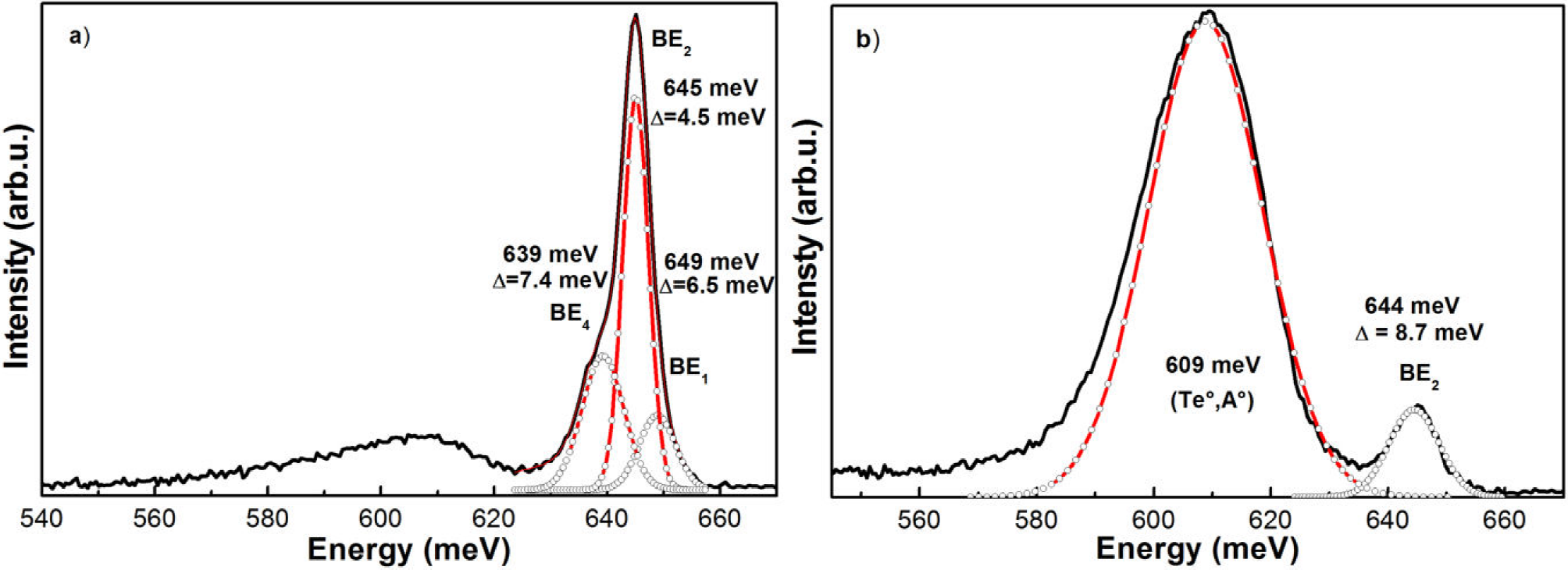
Figure 3. Decomposition of the measured GaInAsSb photoluminescence spectra into individual components (Gaussian shape) for two samples: a) Zn1 and b) Te1. The lines (-o-o-) are their respective fitting. 

Figure 4a illustrates the PL spectra measured at 15 K of n-type samples studied and Fig. 4b shows the PL spectra of p-type ones. As one can observe the PL spectra of Te (or Zn)-doped GaInAsSb have features similar and show the same radiative transitions as in the case of low doping. Therefore, the features observed in PL spectra may be attributed to tellurium (zinc) incorporated in the films. Thus, the increase of dopant concentration above the degeneracy limit results in the substantial broadening of low-temperature PL spectra. The individual band due to the band-to-band (BB) transition, as can be seen in Fig. 4, completely overlap each other at free carrier concentrations. Additionally, at very high concentrations, the low-temperature luminescence band becomes highly asymmetric27.

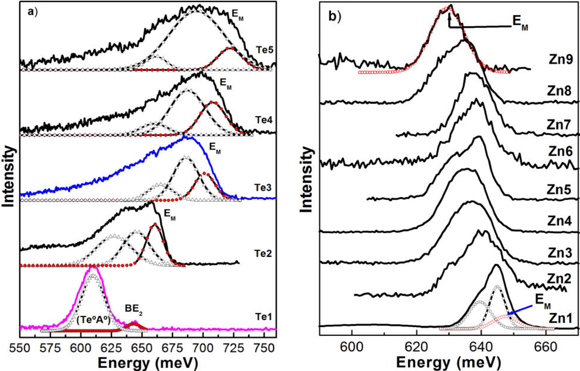
Figure 4. a) Photoluminescence spectra of n-type GaInAsSb as a function of [Sb2Te3] molar fraction in the growth solution at 15 K. The radiative transition band-to-band is renamed by EM to the Te-doped samples. b) PL spectra of p-type GaInAsSb as function of the Zn concentration. They were recorded at 120 mW of excitation power. The lines (-o-o-) correspond to the components of the experimental LT-PL spectra obtained by deconvolution by Gaussian curves. The radiative transition ban-to-band is renamed by EM to the p-type samples. 

At low doping concentration, the donor (acceptor) impurity energy could be treated as a δ function. The low temperature PL spectrum of the non-degenerate materials could be explained by band-to-band (BB) and band-to-acceptor (BA) radiative transitions, as schematically is illustrated in Fig. 5a, shown for p-type material28. As n (or p)-type dopant concentration is increased; the dopant level spreads into a band on two sides. The heavier the doping, the more the spread, as evidenced from the increase of the FWHM with the increase in dopant concentration incorporated in the layers29. However, as the doping concentration is further increased to a level comparable to the effective density of states in the conduction (or valence) band, the band maximum energy (E M ) in the PL spectrum starts shifting toward higher (or lower) energy side. Some examples are schematically shown in Figs. 5b-c, n-type and p-type.

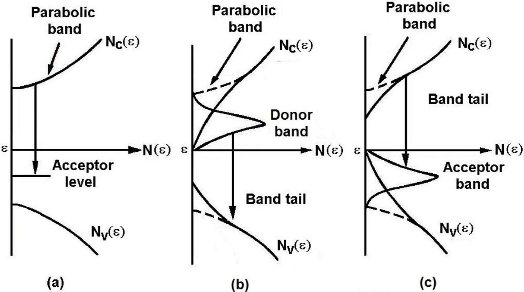
Figure 5. Schematic illustration of the photoluminescence emission from: (a) slightly doped p-type, (b) heavily doped n-type and c) heavily doped p-type samples28

As the n (or p)-type dopant concentration is increased in the crystal; the average spacing of the impurity atoms becomes smaller. When this is close to or less than the Bohr excitonic radius of the impurity states, the majority carriers in the crystal become so numerous that their presence alters the lattice periodic potential. The calculated Bohr excitonic radius to the undoped quaternary alloy is 1.88 nm that was evaluated using the numerical factor mentioned above30. As a result of the high carrier concentration, three effects should be considered for studying the physical properties of the crystal. One of them is the many-body effect that involves ionized donor-electron (acceptor-hole) interaction, electron-electron (hole-hole) interaction and electron-hole interaction. The ionized donor-electron (or ionized acceptor-hole) interaction gives as a result a reduction in the donor (or acceptor) ionization energy and causes the donor (acceptor) level to move toward the conduction (or valence) band edge, E c (or E v ). The electron-electron (hole-hole) interaction shifts E c (or E v ) down (or upward). The electron-hole Coulomb interaction reduces the electron potential energy and causes the conduction (or valence) band edge to move down (or up). The second effect that should be considered is the randomness of the Te (or Zn) atoms that causes fluctuations in the local electrostatic potential and results in the formation of band tail states. Finally, the effect of the carrier degeneracy should also be considered as the Maxwell-Boltzmann statistics will be replaced by the Fermi-Dirac statistics in the case of degenerate semiconductors.

As can be observed in Fig. 4a, PL spectra of Te-GaInAsSb as the dopant concentration is increased the peak EM is shifted to higher energies in all investigated dopant range, this indicates that the PL spectra come from the direct band-to-band or direct impurity-to-band transitions following the k conserving rule. Unlike the photoluminescence spectra of Zn-GaInAsSb have a particular behavior, as can be seen in Fig. 4b, the main radiative band EM in the LT-PL spectra shifts toward lower energies (redshift) as the Zn molar fraction is increased in growth solution from 0-2.325 x 10⁻⁴. This indicates that photoluminescence has the same radiative transitions, as above. The spectral shape of the PL emission band is almost symmetrical. The asymmetry of the spectrum observed at higher Zn molar fraction, sample Zn8, in Fig. 4b strongly indicates that effective band-to-band or effective band-to-acceptor transitions dominate the emission across the energy gap breaking the k conservation31,32. The steep slope characterized by the exponential decay, exp(-ω/Et), of the luminescence on the high-energy side is caused by a decrease in the hole population below the Fermi energy levels. Whereas the smooth slope on the low-energy side closely follows the relationship, I(Et-ω)1/2 33 where E t is the threshold energy of the band in Fig. 3 and I is the spectral intensity at the photon energy ω. In Table II are shown the results of the energetic positions of the band E M obtained by deconvolution of the PL spectra of the studied samples.

In order to compare the observed photoluminescence peaks with calculated transitions in high level of dopant concentration. It is necessary to include not only the usual band filling effect but also band gap shrinkage due to the exchange interaction among free carriers as well as the band tailing effect due to the Coulomb interaction of the free carriers with ionized impurities interaction. All the above-mentioned interactions are calculated taking into account the nonparabolicity of the conduction and valence bands, which result in a concentration-dependent effective mass. The three band Kane’s model34 has been used for the calculation of concentration-dependent effective mass. Kane’s model considers the interaction of the conduction band with the valence band, separated by the band-gap energy E g from the former. The valence band itself is composed of two bands with the energy separation of the spin-orbit split-off energy Δ. At first, one shall assume that the conduction band and valence bands in Ga0.87In0.13As0.14Sb0.86 are described by the following equation:

E'(E'-Eg)(E'+Δ)-2k2P2(E'+2Δ/3)=0 (1)

where E'=E-2k2/2m0, which is true at very high (low) energies in conduction (or valence) band, m 0 is the free electron (or hole) mass, is Planck’s constant, k is the wave number, P is the momentum matrix element, E g is the band-gap energy of undoped Ga0.87In0.13As0.14Sb0.86 and Δ is the spin-orbit split energy. Expanding the solution of Eq. (1) in power of k up to the order k 4, as has been proposed by Bose et al.35, gives the following expressions for the energy of conduction (valence) band as measured from the bottom (or top) of the conduction (or valence) band:

EC=2k22me*+(αcEg)(2k22me*)2Ev=-2k22mh*-(αvΔ)(2k22mh*)2 (2)

The second term on the right hand side of Eqs. (2) depicts the deviation of the E - k dispersion from the ideal parabolic nature. Introducing the dimensionless nonparabolicity factors α’s given by

αc=-(1-me*m0e)2(1+4Δ/3Eg+2Δ2/3Eg2)(1+Δ/Eg)(1+2Δ/3Eg)αv=-2(1-mh*m0h)2(1+Δ/Eg)2(1+2Δ/Eg)9(1+2Δ/3Eg)2 (3)

These terms are named the nonparabolicity factors. Thus, calculating the concentration-dependence effective masses, with the following numerical values of Ga 1-x In x As y Sb 1-y band structure parameters: me*/ m0e=0.0354, mh*/m0h=0.433 36, Eg(14K) = 0.653 eV 37, Δ=0.715 eV36, one can obtain αc=-0.820 and αv=-0.3364. It appears that the nonparabolicity factors are almost temperature independent. Therefore, one can write the equation for the energy within the conduction and valence bands in the following form:

Ec=E0c-0.820(E02/Eg)Ev=E0v+0.3364(E02/Δ) (4)

where E0c=2k2/2m0e* and E0v=-2k2/2m0h*. These equations are valid for highly degenerated materials, which allows to write concentration-dependence effective mass for electrons and holes in nonparabolic conduction and valence bands of the GaInAsSb alloy as:

m*(n)=0.0354m0e(1-23.136×10⁻¹⁴n2/3)-1m*(p)=0.433m0h(1-7.956×10-15p2/3)-1 (5)

These concentration-dependent effective mass expressions allow one for obtaining a useful expression for the Fermi energy of nonparabolic bands in terms of carrier concentration. It has been demonstrated for InP that the Fermi energy calculated by exact method using Fermi integrals differs only at low concentrations of the Fermi energy of nonparabolic bands obtained using the mathematical expressions above mentioned27. For high dopant concentrations, they agree very well with calculated values for the case of nonparabolic bands. Using the early obtained results and the energies of the bands EM for high levels of carrier concentrations, one may estimate the majority carrier concentration, which show a good agreement with the results obtained with the SIMS measurement38. In order to do this, it is necessary to include not only the usual band filling effect but also the band gap shrinkage due to the exchange interaction among free carriers as well as the band tailing effect due to the Coulomb interaction of the free carriers with ionized impurities interaction. All the above mentioned interactions are calculated taking into account the non-parabolicity of the conduction (or valence) band, which results in a concentration dependent effective mass. It is assumed that the hole distribution is highly degenerate, whereas the electrons (holes) introduced by optical generation occupy the states at the very bottom (top) of the conduction (or valence) band. Therefore, to a good approximation, the energy of the photoluminescence band EM arising from band-to-band (BB) transitions would be given by28,39:

EM(n)=Eg0+EFe'(n)-Ece(n)-Ecc'(n)EM(p)=Eg0-EFh'(p)+Ech(p)-Ecc'(p) (6)

Where Eg0,E'Fe(E'Fh),ECC' and ECe(ECh) are: the band gap of undoped GaInAsSb at 15 K; the Fermi energy for non-parabolic bands for electrons or holes; the electron (hole)-impurity interaction40,41; and the exchange interaction among free carriers42, respectively. These equations can be used to estimate the carrier concentration in the samples, in fast form and without using a destructive technique. Here, it has been supposed that Eq. (6) might also be valid at low concentration to estimate the free carrier concentration in the whole investigated range. The carrier concentration was measured through the low temperature PL spectra and fitting the PL peak with the band-filling model, which takes into account the shift of the Fermi energy towards the conduction (or valence) band as the donor (or acceptor) concentration increases. These results suggest that the Te (or Zn) atoms are incorporated in the samples as donor (or acceptor) impurities. The obtained results are presented in Tables I and II and in Fig. 6, which are in agreement with the reported in the literature43,44.

Figure 6. a) Electron concentration as a function of the tellurium molar fraction in GaInAsSb and b) hole concentration as a function of the zinc molar fraction in the quaternary alloy Ga0.86In0.14As0.13Sb0.87 

4. Conclusions

In order to summarize, in this work we have presented a systematic study of doping by tellurium and zinc in Ga0.87In0.13As0.14Sb0.86 epitaxial layers grown on (100) GaSb substrates by LPE. The epilayers studied were doped with Te and Zn in a broad range from low to high concentration. Raman spectra show two phonon bands, which may be assigned to the GaAs and (GaSb + InAs) mixture modes. The frequency of the former mode slightly decreases and the frequency of the latter decreases with increasing the dopant concentration. For low doping levels, the PL spectra show the presence of exciton-related transitions with a small FWHM value (7 meV), which is evidence of good crystalline quality of the layers. For higher doping levels, the PL spectra exhibit band-to-band and band-to-acceptor transitions, which merge in a broad band as the Te (or Zn) doping increases. An important result of the analysis is that the non-parabolicity of the conduction or valence band has to be taken into account in calculating the peak position of photoluminescence spectra at degenerate concentrations and in estimating the electron (or hole) concentration for the grown samples. The predictive model for the band gap narrowing has been applied to GaInAsSb, which is in good agreement with experimental results.

References

1. D.C. Tran. G.H. Siegel, Jr., B. Bendow, Lightwave Technol. (Special Issue on Low-Loss Fibers) LT-2 (1984) 566-586. [ Links ]

2. G. B. Stringfellow, J. Cryst. Growth 58 (1982) 194-202. [ Links ]

3. K. Nakajima, K. Osamura, K. Yasuda, Y. Murakami, J. Cryst. Growth 41 (1977) 87-92. [ Links ]

4. M. Dolginov, D. G. Elisev, A. N. Lapshin, M. G. Milvidskii, Cristal Tech. 13 (1978) 631-638. [ Links ]

5. N. Kobayashi, Y. Horikoshi, C. Uemura, Jpn. J. Appl. Phys. 18 (1979) 2169-2170. [ Links ]

6. H. Kano. S. Miyazawa, K. Sugiyama, Jpn. J. Appl. Phys. 18 (1979) 2183-2184. [ Links ]

7. J.C. DeWinter, M.A. Pollack, A.K. Srivastava, I.I. Zyskind, J. Electron. Mater. 14 (1985) 729-747. [ Links ]

8. J.L. Lazzari, E. Tournié, F. Pitard, A. Joullié, Mat. Sci. and Eng. B 9 (1991) 125-128. [ Links ]

9. P. K. Bhattacharya, T. Matsumoto, S. Subramanian, J. Cryst. Growth 68 (1984) 301-304. [ Links ]

10. T. Nakanisi, J. Crystal Growth 68 (1984) 282-294. [ Links ]

11. T.C. McGlinn et al., Phys. Rev. B 33 (1986) 8396-8401. [ Links ]

12. J. Díaz-Reyes, J.G. Mendoza-álvarez, P. Rodríguez-Fragoso, E. López-Cruz, J.L. Herrera-Pérez. Vib. Spectrosc. 68 (2013) 109-114. [ Links ]

13. J. Menendez, A. Pinczuk, J. Bevk, J.P. Mannaerts, J. Vac. Sci. Technol. B 6 (1988) 1306-1309. [ Links ]

14. F. Frost, G. Lippold, A. Schindler, F. Bigl, J. Appl. Phys. 85 (1999) 8378-8385. [ Links ]

15. R. Loudon, Adv. Phys. 13 (1964) 423-482. [ Links ]

16. D. Olego, M. Cardona, Phys. Rev. B 24 (1981) 7217-7232. [ Links ]

17. G. Abstreiter, E. Bauser, A. Fisher, K. Ploog. Appl. Phys. 16 (1978) 345-352. [ Links ]

18. M. Qi, M. Konagai, K. Takahashi. J. Appl. Phys. 78 (1995) 7265-7268. [ Links ]

19. T. Yuasa et al., Phys. Rev. B 33 (1986) 1222-1232. [ Links ]

20. T. Yuasa, M. Ishii, Phys. Rev. B 35 (1987) 3962-3970. [ Links ]

21. M.V. Belousov, A.T. Gorelenok, V.G. Gruzdov, V.Y. Davydov, I.Y. Yakimenko, Tech. Phys. Lett. 19 (1993) 33-35. [ Links ]

22. J. Díaz-Reyes et al., J. Phys.: Condens. Matter 15 (2003) 8941-8948. [ Links ]

23. S. Iyer, S. Hegde, A. Abul-Fadl, W. Mitchel, Phys. Rev. B 47 (1993) 1329-1339. [ Links ]

24. E.T.R. Chidley et al., Semicond. Sci. Technol. 6 (1991) 45-53. [ Links ]

25. J. Díaz-Reyes, M.L. Gómez-Herrera, J.L. Herrera-Pérez, P. Rodríguez and J.G. Mendoza-álvarez, Cryst. Growth Des. 9 (2009) 3477-3480. [ Links ]

26. M. Ichimura, K. Higuchi, Y. Hattori, T. Wada, N. Kitamura, J. Appl. Phys. 68 (1990) 6153-6158. [ Links ]

27. M. Bugajski and W. Lewandowski, J. Appl. Phys. 57 (1985) 521-530. [ Links ]

28. J. Díaz-Reyes, P. Rodríguez-Fragoso, J.G. Mendoza-álvarez. J. Lumin. 134 (2013) 126-131. [ Links ]

29. G.B. Scott, G. Duggan, P. Dawson, G. Weimann, J. Appl. Phys. 52 (1981) 6888-6894. [ Links ]

30. U.E.H. Laheld, F.B. Pedersen, P.C. Hemmer, Phys. Rev. B 52 (1995) 2697-2703. [ Links ]

31. C.W. Chen, M.C. Wu, S.C. Lu, C.C. Chang, Jpn. J. Appl. Phys. Part 1 32 (1993) 2725-2730. [ Links ]

32. Y. Jiang De-Sheng, K. Makita, Ploog, H.J. Queisser, J. Appl. Phys. 53 (1982) 999-1006. [ Links ]

33. H. Barry, E.W. Williams, in: R.K. Willardson, A.C. Beer (Eds.), Semiconductors and Semimetals, Vol. 8, Academic, New York, 1972. (Chapter. 5). [ Links ]

34. E.O. Kane, J. Phys. Chem. Solids 1 (1957) 249-261. [ Links ]

35. M.K. Bose, K. Midya, C. Bose, J. Appl. Phys. 101 (2007) 054315-1 to 5. [ Links ]

36. M.P. Mikhailova, in Handbook Series on Semiconductor Parameters, vol. 2, M. Levinshtein, S. Rumyantsev and M. Shur, ed., World Scientific, London (1999) 180-205. [ Links ]

37. J. Díaz-Reyes, J.L. Herrera-Pérez, M.L. Gómez-Herrera, J.A. Cardona-Bedoya, J.G. Mendoza-álvarez, Appl. Surf. Sci. 238 (2004) 400-404. [ Links ]

38. Y.E. Bravo-García et al., Superficies y Vacío 25 (2012) 175-178. [ Links ]

39. J. Díaz-Reyes, J.G. Mendoza-álvarez and M.L. Gómez-Herrera, J. Phys.: Condens. Matter 18 (2006) 10861-10869. [ Links ]

40. C.J. Hwang, Phys. Rev. B 2 (1970) 4117-4125. [ Links ]

41. H.C. Casey, Jr. and M.B. Panish, Heterostructure Laser, Part 1: Fundamental Principles (academic, New York, 1978) 135. [ Links ]

42. J. Camassel, D. Auvergne and H. Mathieu, J. Appl. Phys. 46 (1975) 2683-2689. [ Links ]

43. R.M. Biefeld, J.G. Cederberg, G.M. Peake, S.R. Kurtz, J. Cryst. Growth 225 (2001) 384-390. [ Links ]

44. C.A. Wang, H.K. Choi, D.C. Oakley, G.W. Charache, J. Cryst. Growth 195 (1998) 346-355. [ Links ]

Received: September 07, 2016; Accepted: October 28, 2016

Creative Commons License This is an open-access article distributed under the terms of the Creative Commons Attribution License