Research
Growth of doped PbS:Co2+ nanocrystals by Chemical Bath
O. Portillo-Morenoa
*
R. Gutiérrez-Péreza
M. Chávez Portilloa
M.N. Márquez Speciaa
G. Hernández-Télleza
M. Lazcano Hernándeza
A. Moreno Rodrígueza
R. Palomino-Merinob
E. Rubio Rosasc
aMaterials Science Laboratory, Fac. Ciencias Químicas, Autónoma de Puebla, P.O. Box 1067, Puebla, 72001, Pue. México.
bFac. Ciencias Físico Matemáticas, Posgrado en Física Aplicada, Universidad Autónoma de Puebla, México, 72001.
cCentro Universitario de Vinculación y Transferencia de Tecnología, Universidad Autónoma de Puebla, Ciudad Universitaria, 72001.
ABSTRACT
Nanocrystalline PbS films grown by chemical bath at T = 40 ± 2 oC onto glass slides were modified by in situ Co2+ -doping and their structural and optical properties were examined. By FT-IR spectra, a sharp stretching mode can be seen at ~1384 cm-1 due to the vibration mode of CO32 ions. XRD patterns shown the growth on the zinc blende crystalline face. The grain size was determined by using X-rays diffractograms and was found at ~28 nm and ~13 - 25 nm for undoped and doped samples, respectively. Optical absorption spectra was used for calculating the energy band gap, and displayed a shift in the ~1:21 - 2:21 eV range, associated with quantum confinement effect. Raman peaks at ~ 210, 271, and 451 cm-1, corresponding to a 1LO phonon mode, a two-phonon process, and a 2LO phonon mode respectively were also recorded. The surface and grain size of the films were measured by AFM studies.
Keywords: Thin films; nanocrystals; quantum; confinement effect; doping
PACS: 71.20.Nr; 68.55.A; 64.70.kg
1. Introduction
Semiconductors obtained by combining elements from IIB and VA groups, such as CdSe, CdS, PbS,
ZnO, etc., are interesting systems demonstrating quantum-confinement effects as the
nanocrystal size corresponds to the Bohr exciton radius. Some reports have evidenced
that quantum confinement in thin films produced by reduction grain size (GS) afford
changes in electro-optical properties that can be exploited in a broad range of
applications 1. Hence, doping of
semiconductors have shown different optical and structural changes in Lead
Chalcogenide materials. Furthermore, there is an increasing interest into deposition
of ternary derivative materials due to their potential tunable band-gap energy
(Eg), by means of the growth parameters such as reaction temperature
and concentration of reactive precursors by systematic doping2,3. Several methods for the preparation of PbS
nanocrystals have been reported in recent years such as microwave and sonochemical
methods4, chemosyntesis 5, etc. However, most of the reported
studies have been focused on the deposition of ternary derivatives material on thin
films as Pb1-x CoxS6, Pb1-x
NixS 7,
Pb1-xCdxS 8. In this regard, PbS nanocrystals
with GS dimensions in the 5-20 nm range are of technological interest for advanced
optoelectronic applications, showing a stronger quantum confinement effect when the
crystal size matches the dimension of Bohr exciton 9. In the present work, PbS and PbSCo2+ -
doped films were prepared by a green approach: chemical bath (CB), in order to
investigate their structural and optical properties. FTIR spectra were recorded
using a Perkin Elmer spectrophotometer in the 500-4000 cm-1 wavelength
region. The crystalline structure characterization was carried out by X-Ray
diffraction (XRD) patterns registered in a Bruker D8 Discover Diffractometer, using
the Cu Kα line. The optical absorption spectra, measured in a Varian CARY
spectrophotometer, allowed to calculate Eg. A micro-Raman Lab Ram- Idler
apparatus with an excitement line of 514.5 nm wavelength Ar laser for Raman
spectroscopy was used. Images of the surface were obtained by atomic force
microscopy (AFM) with Nano-scoped E model contact mode instrument from UGC-DAE
consortium of Scientific Research, Indore.
2. Chemical reactions and experimental procedure
We carried out a simple model of chemical reactions in the preparation of undoped and doped PbS films with a Co2+ solution determined by employing the reported cell potential values in basic media 7,10,11
SC(NH2)2+3OH-↔CO32-+S2-+7H+
(1)
CH3 COO- ion is generated by dissociation of Pb(CH3CO3) according to:
Pb(CH3COO)2↔Pb2++2CH3COO-
(2)
The coordinate complex ion [Pb(NH3)4]2+ generated inderectly in our working conditions slowly release Pb2+ ions 7:
[Pb(NH3)4]2++S2-↔PbS+4NH3ΔG0=+362.88KJ
(3)
The doping that generates Co2+ ion has the following chemical equilibrium:
Co(OH)2↔Co2++2OH- ΔG0=+140.08 KJ
(4)
Finally, the overall reaction is:
[Pb(NH3)4]2++S2-Co(OH)2↔PbSCo2++4NH3+2OH-ΔG0=+502.96KJ
(5)
Chemical equilibrium is associated with changes in Gibbs free energy as the dopant ion is incorporated in ionic form in the PbS samples.
For the preparation of polycrystalline PbS thin films onto glass substrates, both undoped and doped samples (volume-solution V[Co2+] containing the doping Co2+ chemical agent) grown by CB, PbS films three different levels of doping V[Co2+] were obtained by in situ addition of 10, 20, 30, mLs in the solution for PbS growth: Pb(CH3CO3)2 (0.01M), KOH (0.1M), NH4NO3 (1.2M), SC(NH2)2 (0.1M). The solutions were mixed and the final solution kept at 40 ± 2 °C during 1.0 h(3). The optimal doping concentration V[Co2+] Co(NO3)2 (0.125 M) was determined after several trials when the films had attained good adherence. This solution is routinely added to the reaction mixture during the growth of the PbS films. The samples were labelled as PbS for the undoped sample and PbSCo10,…, PbSCo30 for the doped samples.
3. Results and discussion
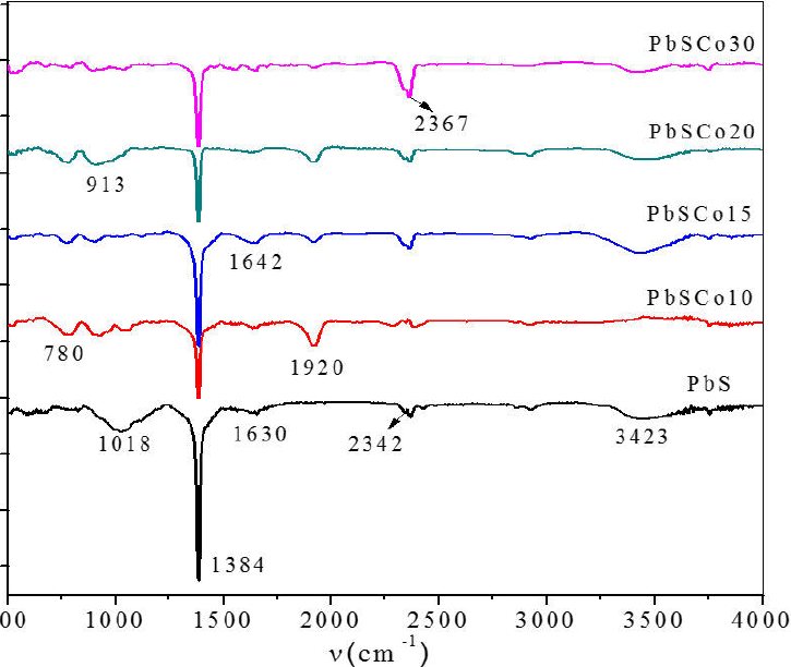
FT-IR spectra of PbS and PbSCo2+ -doped films are displayed in Fig. 1. The main spectral features are similar, excepting the intensity of the absorption band of CO32- at ~ 1384 cm-1; the band located at ~ 1921 cm-1 was assigned to one of the fundamental frequency of COO- bonds12 (see Equations (1) and (2) for the processes involved in the COO- and CO32- formation). The broad absorption band at the ~ 3423 cm-1 region can be attributed to stretching of the -OH groups of defective sites and the physically adsorbed water molecules. The bands at ~ 1642 and ~ 1018 cm-1 were ascribed to the vibration of amine groups 13. The peak at ~ 2342 and ~ 2367 cm-1 are characteristic of COO- and S-H stretching vibrations, confirming the presence of acetate and sulfur ions. The decrease in the peak located at ~ 1384 cm-1, assigned to the CO32- vibration indicates the bonding to the surface of PbS by the carboxyl groups. As a result, the characteristic vibrations for the CO32- ions displayed at 1642 cm-1 and 1630 cm-1 are symmetric bending and stretching modes, respectively. The Pb-S bond is mainly an electrovalent bond, thus the FT-IR spectrum of spectrum of PbS does not show strong bands associated with Pb-S stretching and bending vibration. The bands at ~ 780 and ~ 920 cm-1 were not identified, but may be associated with Pb-Co bonds. When V[Co2+] is added and PbS are supplied into crystals, the interactions reduce as some of PbS will react to forms nanoparticles. A comparison of these spectra clearly shows that many CH3-COO-, OH- and CO32- ions remain on the surface of nanocrystals, which were removed by washing with distilled water and drying the films with an hot air flow.
We associate this peak broadening considering the Pb2+ ion radius compared to the dopant ionaccording to: Pb2+ = 1.20 Å, S2- = 1.84 Å and Co2+ = 0.83 Å. In a previous report7, we proposed the following that for a relative low concentration of Co2+ ions, a majority can be located in (i) Pb2+ vacancies sites, which otherwise would be empty (ii) in Pb2+ sites causing the appearance of Pb2+ interstitial sites, and (iii) in interstitial positions 3. It can be mentioned that the stable crystal structure of PbS, when Co2+ occupies more sites of Pb2+ in the host lattice, afford an increase in internal strain. Through this gradual occupation in vacancies and interstitial sites of the ions in the crystal lattice, the GS is reduced to release the strain. As the Co2+ concentration is increased, the diffraction peaks become broader due to the reduction in the GS. Inset in Fig. 2 shows the GS vs V[Co2+] for all samples corresponding to the (200) plane. The GS of ~ 28 nm for PbS and PbSCo10 layers decrease ~ 13 nm, however GS increase almost linearly with increasing V[Co2+]. The effect of the GS by the doping effect has been reported in films of doped samples 2,3,5.
The absorbance spectra vs wavelength (nm) of all the films is shown in Fig. 3, in order to compare the changes produced by the dopant. These absorption spectra show an abrupt change in the doped samples compared to undoped PbS. The spectra of PbSCo20 and PbSCo30 layers exhibited an absorption onset of ~ 550-700 nm, these bands are shown with a blue strip. These exciton bands were at- tributed to a 1Se - 1Sh transition, this effect is associated with quantum confinement produced by the decrease of GS14. However, Todd et al. reported three sharp peaks in the absorption spectra of the lowest exciton transitions calculated for particles of 1.5 nm radius 15. The absorption spectra in the visible light region presents a component at ~ 587 nm, assigned to the spin and electric-dipole-allowed 4A2 (F) → 2A1 (G), 4A2(F) → 2T1(G), and 4A2 (F) → 2E(G) transitions, respectively. All doped samples have weak absorption in the visible and NIR regions, and the intensity of the absorption band increases with V[Co2+] increasing. Such augmentation is associated with the increasing of Co2+ ions located in tetrahedral sites of PbS. The observed structures in the optical absorption spectra of PbSCo samples are similar to those observed in other materials, both in bulk as well as in the nanocrystalline form16.
A comparison of the effect of nanocrystalline size on electron-phonon coupling for PbS quantum
dots with controlled but variable particle size in PbSCo grown by CB has not been
reported so far. The plot of Eg vs. V[Co2+] for all samples is displayed in Fig.
4. It can be observed a Eg = 1.21 eV for the PbS sample. Bulk
PbS (Eg = 0.41 eV) and bulk CoS (Eg = 1.15 eV) are expected to
vary Eg between 0.41 and 1.15 eV, however in these spectra such change
are not appreciated 6. The
confinement effect appears as a shift in the edge of the absorption spectra and the
absorption to lower wavelengths, due to the decrease in GS and number of defects. It
is clearly seen, from the optical spectrum, an absorption edge shift towards a lower
wavelength in doped films. Thus, the observed modification of PbSCo samples showed
the existence of quantum confinement. The experimentally observed Eg
values for the shift indicated an alloying in nanocrystalline PbS 17,18. The fundamental optical transition of doped
films (Eg = 0.41 eV) is not observed in these doped films, because of
complete mixing of PbS with Co2+ ions yielding an unique intermetallic
compound of PbxCo1-x S type
5. The Eg in our
work for samples in the ~ 1.2-2.2 eV range shows the extent of quantum size effect
in the nanoparticle films. A similar shift observed in the position of the excitonic
peak towards higher energies in CdSe crystallites has been explained due to a
decrease in crystallite size 19.
Inset in Fig. 4 shows the plot of Eg
vs. (αhγ)2 of PbS-PbSCo. In our case, the introduction
of Co2+ ions into the PbS lattice induced a increase of strain. Such
strain in PbSCo samples tends to reduce GS.
Raman spectra is shown in Fig. 5. The spectra are compared each other to observe the differences produced by the Co2+ dopant. Similar peaks in these spectra at 148, 192, 201, 281, 442 cm-1 are observed along with a prominent band at ~ 148 cm-1. Peaks at ~ 210, 271, 451 cm-1 can also be observed, corresponding to a 1LO phonon mode, a two-phonon process, and a 2LO phonon mode, respectively20. In addition, the peak or shoulder at ~ 192 cm-1 has been identified to be due to the SP mode, and its intensity greatly increases with decreasing crystal size.
These results confirm those obtained by optical absorption and XRD. They are influenced by
some parameters, such as atomic masses of Pb, S and Co atoms and vibration constant
of bonding atoms residing in the lattice. Our measurements on samples from different V[Co2+] exhibited a variation on the intensity of these broad bands, so in these
films, the effect of dopant is clear and can be seen with variations of the
intensities of the bands. The reason for this behavior is associated with the
stoichiometry of PbS caused by the gradual incorporation of the Co2+
ions. Raman bands in the high-frequency two-phonon region can also be observed at ~
450 cm-1
7.
The 3D images of atomic force microscopy (AFM) are showed in Fig. 6 for: (a) PbS, in this image the surface morphology exhibited agglomerates with pyramidal geometry grown on the flat surface, and no holes or islands are observed. (b) in this 3D image of PbSCo20 film, the disappearance of conglomerates displayed an almost flat surface. In this sample the effect of dopant can be clearly seen. Images of all doped samples are not shown because there are few significant changes compared to the one shown here.
4. Conclusions
The effect of VCo2+ on the morphological, crystal structure and optical band gap properties of thin films has been investigated. The composition study showed that these films were stoichiometric, with slight variation in sulfur deficiency. The XRD pattern revealed that films are crystalline with average grain size decreased as VCo2+ increased. These films also displayed large final thickness and their surface morphologies were composed of small grains with an approximate size of 27-12 nm. Optical absorbance measurements indicated the existence of direct transition with corresponding energy gap in a 2.1-2.4 eV range. These films also exhibited a good transmittance of about 60% in visible and near infrared regions, allowing their potential use as a window layer in high efficiency thin films solar cells. In summary, we have found an efficient process to introduce Co2+ ions into the PbS structure with, practically, no large damage to the lattice.
Acknowledgments
The authors thank Lic R. Villegas Tovar from BUAP Library from their collaboration in the achievement of this research.
REFERENCES
1. E.O. Chukwuocha, M.C. Onyeaju, T.S.T. Harry, Condensed Matter Physics 2 (2012) 96-100.
[ Links ]
2. K. Rakesh, H.A. Joshi, H.K. Sehgal, Appl. Surf. Sci. 14 (2003) 809.
[ Links ]
3. R. Palomino Merino et al., J. Nanosci. Nanotech. 14 (2014) 5408.
[ Links ]
4. H. Khallaf, C. Guangyu, O. Lupan, L. Chow, S. Park, A. Schulte, Appl. Surf. Sci. 255 (2009) 4129.
[ Links ]
5. S.B. Pawar, J.S. Shaikh, R.S. Devan, Y.R. Ma, P.N. Bhosale, P.S. Patil, Appl. Surf. Sci. 258 (2011) 1869.
[ Links ]
6. N. Mathur, R.K. Joshi, G.V. Subbaraju, H.K. Sehgal, Physica B 23 (2004) 56.
[ Links ]
7. O. Portillo Moreno et al., ISRN Nanotechnology, 1 (2012).
[ Links ]
8. H.M. Upadhyaya, S. Chandra, J. Mat. Sci 29 (1994) 2134.
[ Links ]
9. J.B. Biswal, N.V. Sawant, S.S. Garje, Thin Solid Films 518 (2010) 3164.
[ Links ]
10. A.J. Bethune, N.A.S Loud. In Standard Aqueous Potential and Temperature Coefficients at 25°C, C.C. Hampel, Skokie, II. 1969.
[ Links ]
11. M. Chávez Portillo et al., Rev. Mex. Fis. 61 (2015) 83.
[ Links ]
12. C. Li, Y. Zaho, F. Li, Z. Shi, S. Feng, Chem. Mat. 22 (2010) 1901; Froment, M. Lincot, D. Electrochem. Acta 40 (1995) 1293.
[ Links ]
13. D.H. Lee, R.A. Condrate, J.S. Reed, J. Mater. Sci. 31 (1996) 471.
[ Links ]
14. Y. Wang, A. Suna, W. Mahler, R. Kasowsky, J. Chem. Phys. 87 (1987) 7315.
[ Links ]
15. F.J. Torres, U.R. Rodríguez Mendoza, V. Lavin, E.R. de Sola, J. Alarcón, J. Non-Cryst. Solids 353 (2007) 4093.
[ Links ]
16. L. Nataf, F. Rodríguez, R. Valiente, Phys. Rev. B 86 (2012) 10010.
[ Links ]
17. R. Kostic et al., Opt. Mat., 30 (2010) 1177.
[ Links ]
18. M.J. Ventura, C. Bullen, M. Gu, Opt. Express 15 (2007) 1622.
[ Links ]
19. A. Rivera Márquez et al., phys. solidi state 188 (2001) 1059.
[ Links ]
20. J.P. Ge, J. Wang, H.-X. Zhang, X. Wang, Q. Peng, Y.-D. Li, Chem. Eur. J. 11 (2005) 1889.
[ Links ]


 nueva página del texto (beta)
 Inglés (pdf)
 Artículo en XML
 Referencias del artículo
 Enviar artículo por email
 Citado por SciELO
  Similares en
SciELO
Similares en
SciELO 
 Permalink