


 text new page (beta)
 English (pdf)
 Article in xml format
 Article references
 Send this article by e-mail
 Cited by SciELO
  Similars in
SciELO
Similars in
SciELO 
 Permalink
PACS: 71.70.Ej; 72.25.Dc; 73.21.Hb; 73.23.Ad
1. Synopsis of Fundamentals and Motivation
For many actual practical solutions and technological applications, due to the impressive development of low-dimensional electronic and optoelectronic devices, it is drastically important to include the valence-band mixing1, i.e. the degree of freedom transverse to the main transport direction, whenever the holes are involved. Previous theoretical studies had focused this topic in resonant tunneling2 and had pointed up its relevance for experimental and technological applications1 . If the electronic transport through these systems, engage both electrons and holes, the low-dimensional device response threshold depends on the slower-heavier charge-carrier’s motion through specific potential regions3. It is unavoidable to recognize that in the specialized literature there is plenty of reports studying several physical phenomena derived from hole mixing effects and strain, via standard existing methods. Some authors had managed to determine optimal situations in a resonant tunneling of holes under internal strains, disregarding scattering effects and assuming a spatial symmetry for a constant potential4 . A first-principles study on valence-band (VB)-mixing, established a non-linear response for a pseudo-potential in series of the atomic distribution function5 . Over the past few decades VB-mixing and/or strain had been extensively studied in several nanostructures ranging from quantum wells4,6,7,8 to quantum wires9,10 and to quantum dots11. However, just a few reports are available regarding the very evolution itself of the effective potential due to several causes, as a central topic of research. We do not focus in the present paper on the VB-mixing and strain effects problem themselves, but rather on the evolution of the effective potential when tuning both effects and on their possible influence over the scattering properties. We hope to make some progress in the understanding of the underlying physics as well as determining whether or not the VB-mixing and strain are competitor mechanisms in the evolution of the effective potential. Few direct measurements -if any- are available because they have not been usually carried out on the subject. We hope to trigger further experimental works on hole-coupling effects and strain phenomenon in the same setup, even in complementary fields whenever scattering events of mixed holes through stressed heterostructures are involved.
Earliest striking elucidations due to Milanović and Tjapkin for electrons,12 and recalled much later by Pérez-Álvarez and García-Moliner for a fully unspecific multiband theoretical case14, are fundamental cornerstones in this concern. The metamorphosis of the effective band offset potential Veff, “felt" by charge carriers depending on the transverse momentum value, is a very persuasive workbench to graphically mimic, the phenomenon of the in-plane dependence of the effective mass, widely known as the VB-mixing for holes. In a few words, a hole band mixing is crucial for bulk and low-dimensional confined systems possessing quantal heterogeneity, as shall be discussed in this paper, similarly to the single-band-electron problem12 and somehow to the unstrained multiband-hole problem13 . Particularities of the appealing evolution features of Veff for holes, in the presence of gradually increasing VB-mixing under strain and assuming their effects are well understood, could be of interest for condensed-matter physicists, working in the area of quantum transport through standard quantum barrier(QB)-quantum well(QW) layered systems in multiband-multichannel models.
As common assertion, the Veff input value derives from bulk band offset lineup as long as the transverse momentum (κT) values are negligible14 . For finite κT, this assertion is no longer valid and the mixing effects appear. Such phenomenology is a typical non-linear κT effect, whose most striking consequence is the predicted interchange of functions between QW and QB12,14 . Past theoretical studies have emphasized the existence of energy shifted bound states under κT-dependent Veff15 and a larger reduction for Veff as a function of κT for light holes (lh) in respect to that of heavy holes (hh) . These former works5,12,14,15,16, were motivating enough and put us on an effort to develop a more comprehensive vision, of how Veff evolves spatially with κT and strain for hh and lh. This paper is devoted to demonstrate, that Veff profile evolution, QB-QW permutations and bandgap changes, are reliable tools for tuning the response threshold of a layered semiconductor system with spatial-dependent effective mass, and that VB-mixing and stress effects are possible concurrent mechanisms.
Built-in elastic strained layered heterostructures, has been remarkably used in the last decade, for development of light-emitting diodes, lasers, solar cells and photodetectors17. Besides, internal strain may results into a considerable modification of the electronic structure of both electrons and holes, thereby altering the response of strained systems respect to nominal behavior of strain-free designs17 . To account for strain in the present study, we additionally suppose a heterostructure sandwiched into an arbitrary configuration of pseudomorphically strained sequence of QW-acting and QB-acting binary(ternary) alloys. This assumption is motivated by actual technological interest on specific materials and configurations. On a layer-by-layer deposition, whenever the epitaxially grown layer’s lattice parameter matches that of the substrate in the in-plane direction -without collateral dislocations or vacancies- the process is referred as pseudomorphic [see Fig. 1(b)]18 . The last one is standardized and chosen for most day-to-day applications like write-read platforms, such as sound/image players and data-manipulating devices. Our motivation arises from the probable existence of a competitor mechanism able to diminish the effects of VB-mixing on Veff13, or even wipe them out occasionally. Such prediction is not available yet in the specialized literature. The uncommon simultaneous treatment of the strain in the presence of hole-coupling effects remains absent or insufficiently addressed, thereof the scientific merit of the present theoretical attempt regarding earlier specialized reports4,6,7,8,11,13 is warranted.
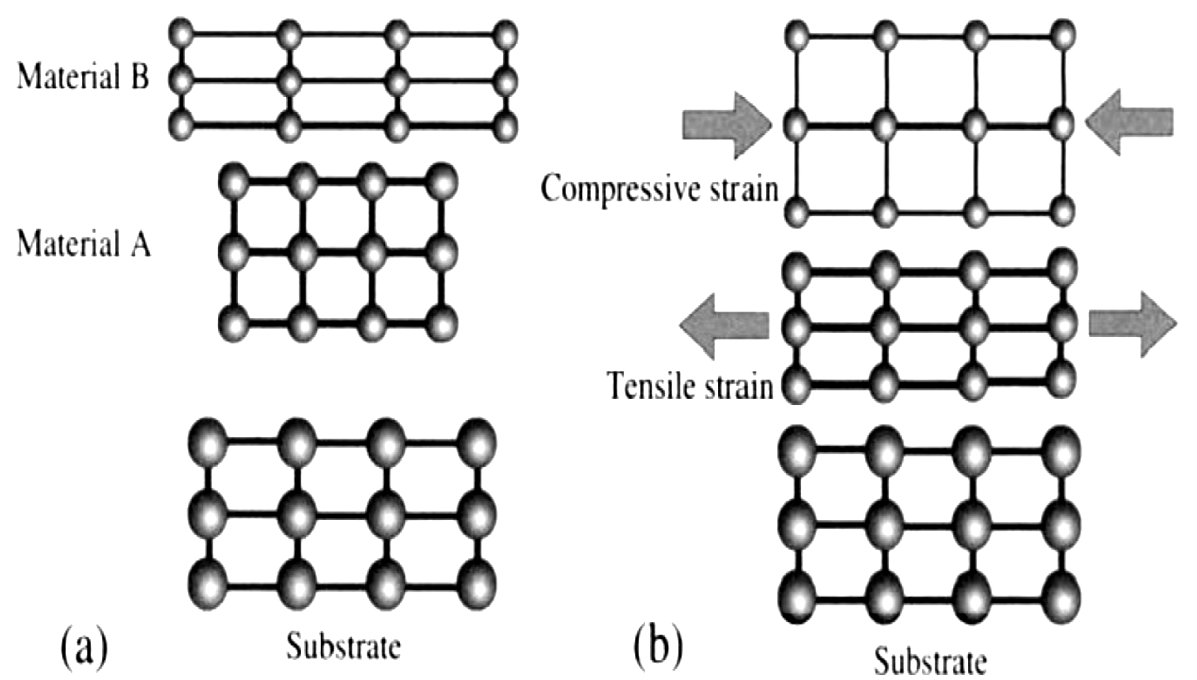
Figure 1 Panel (a) shows the stress-free bulk materials, with lattice parameter al < as smaller (GaAsP), and larger al > as (InGaAs) tan that of the substrate 22. Panel (b) illustrates a schematic representation of a pseudomorphic grown process for a layered heterostructure 18. The material GaAsP is under a tensile strain, while the material (InGaAs) is under compressive strain, as they both are forced to conform the buffer’s lattice constant as of a suitable semiconductor wafer.
The outline for this paper is the following: Sec. 2 presents briefly the theoretical framework to quote the VB Veff for both unstressed and stressed systems. Graphical simulations on Veff evolution, are exposed in Sec. 3. In that section, we discuss highly specialized III-V semiconductor binary (ternary)-compound cases with straight links to real-word technological applications. That section supports the main contribution of the present study and suggests possible applications. Sec. 4, contains the conclusions.
2. Calculation of the effective potential
Commonly, a wide class of solid-state physics problems, related to electronic and transport properties, demands the solution of multiband-coupled differential system of equations, widely known as Sturm-Liouville matrix generalized boundary problem14:
where B(z) and W(z) are, in general, (N × N) Hermitian matrices and is fulfilled Y(z) = -P†(z). In the absence of external fields, standard plane-wave solutions are assumed and it is straightforward to derive a non-linear algebraic problem
called as quadratic eigenvalue problem (QEP)16, since Q(kz) is a second-degree matrix polynomial on the z-component wavevector kz. In the specific case of the well-known (4 × 4) Kohn-Lüttinger (KL) model Hamiltonian, the matrix coefficients of Equation (2) bear a simple relation with those in (1)16:
Then for (4 × 4) KL model, the matrix coefficients of (2) can be cast as:
Here
Bearing direct association to the original matrix dynamic equation, we exclusively focus to
the case when
is an eighth-degree polynomial with only even power of
kz and real coefficients. The
coefficients qi are functions of the
system’s parameters, and q0=det
Based on our, it is straightforward to know whereas kz is oscillatory or not by dealing with (7), and thereof to retrieve the phenomenological characteristics for Veff. To manage complex-valued eigensolutions for (7) as a function of the VB-mixing and strain, we retrieve the root-locus-like procedure 13, provided its robustness when pursuing a simple graphical interpretation for a non-linear eigenvalue problem (2). To our knowledge, just few pure theoretical or numerical applications of the root-locus-like algorithm, particularly for the QEP scenario, have been previously addressed to explicitly describe several standard III-V semiconductor compounds13,19. We acknowledge the advantages of the root-locus-like technique application within the low-dimensional solid state physics13,19 -we may be the first ones- and try to predict unknown phenomenology whenever coupled holes interplay with mutable Veff of the stressed system. For some high specialized zinc-blenda and wurtzite systems, current knowledge of the hole quantum transport mechanism is limited. The present theoretical contribution, claims to shed light on that issue. We think readers will be interested more on how the Veff metamorphosis under VB-mixing and strain could influence their real-world devices, rather than getting involved into the very details of the theoretical model itself. In regard to that concern, we propose a simple and comprehensive modelling procedure for Veff to deal with, and a gedanken-like simulation for a passage of mixed holes throughout a strained-free and strained layered heterostructures. The purpose of that is hardly a hypothetic exercise, but rather pretends to show to condensed-matter theoreticians and to complementary-fields physicists, why a non-mutable Veff under VB-mixing and strain is not acceptable and how they can re-model Veff to improve their own works within similar conditions.
According to prior description for VB-mixing5
and in order to achieve the target of the present study, an effective potential
operator
Next we follow symmetry considerations 20, and solve a Schrodinger-like equation in the (2 × 2) Hilbert reduced-space of the KL model
whose eigensolutions are the expected values for Veff. The
superscript indicates the order of the corresponding matrix. The operator
Strain field may rise questions over their relative effects on the electronic structure and, in particular on the valence-band structure where shape and size of the potential profile lead to stronger hybridization of the quantum states. Lets now examine the effects of the stress in the framework of the KL model Hamiltonian. The existence of a biaxial stress applied upon the plane parallel to the heterostructure interfaces leads to the appearance of an in-plane strain. The effective potential operator
where
is the accumulated strain energy resulting from the tensile or compressive stress acting on the crystal, when an epitaxial layer is grown on a different lattice-parameter substrate. Owing to strictness in formulation22 , we guess that a maximum-quota criterium (11) suffices to achieve the goal posted in Sec. 1. Being independent from κT, a maximized Us was taken for granted to evaluate if there is a real challenger strain effect over VB-mixing’s influence on the metamorphosis of Veff. In (10)-(11), the subscript s stands for strain. In (11) av /b represent the Pikus-Bir deformation/break potentials, describing the influence of hydrostatic/uniaxial strain. Meanwhile ε1,3, are the in-plane, and normal-to-plane lattice displacements, respectively. For commonly used cubic and hexagonal semiconductor compounds, we assume17,18
with as,l the lattice parameter of the substrate and the epitaxial layer, respectively. Though no external stress is considered along the growth direction z, the lattice parameter is forced to change due to the Poisson effect18 . Hence, the normal-to-plane displacement can be cast as
which remains connected to in-plane deformation ε1 via the Poisson radio ν. The last is valid for zinc blende and wurtzite materials.
By changing the material and the growth plane, the value of v modifies. For cubic materials it reads17
while for the hexagonal ones we have17
To quote the parameter
For the sake of completeness of the present theoretical framework, we have derived analytic expressions for the VB-band offset Veff as a straightforward function of the band mixing parameters and the strain energy. In current solid-state physics studies, the later could allow a comprehensive analysis in cubic as well as in hexagonal layered-stressed semiconductor systems, whenever one manages to manipulate the accumulated pseudomorphic strain and mixing effects in a single shoot. We have considered (10)-(11) for solving (9), and thus for zinc blende (cubic) materials it may be cast
being
and
for j = A, B. In these expressions,
Ej stands for the particle
energy in the material j; while
For systems that crystalize in the wurtzite structure have been derived a (6 × 6) effective Hamiltonian
yielding a (6 × 6) block-diagonal Hamiltonian, quite similar in general sense to the reduced-space KL Hamiltonian we had used for the zinc blend heterostructures. The sub-scripts u(l) stand for up(low) respectively, as a resemblance of the up(down) spin-electronic states flavors and have been introduced by Broido and Sham 25, who found alike transformation as (17), but for the (4 × 4) KL model. The (3 × 3) Hilbert reduced-space blocks in (17), satisfy the following symmetry relation
which is an analog to that deduced for the (2 × 2) Hilbert reduced-space of the KL model20. Preserving the same conception
framework posted above, the potential-energy operator
whose blocks fulfil
The up-block of (19) -in the presence of biaxial pseudomorphic strain-, has the general form
while its matrix elements are taken as
together with
On the ground of symmetry relations (18) and (20), the quoting of
and has the solutions
For (22) and (23) we have taken
3. Discussion of results
Unless otherwise specified, the graphical simulations of Veff reported here, were calculated using highly specialized III-V semiconductor binary(ternary)-compound cases for both unstressed and stressed cubic and hexagonal systems. The present numerical simulations consider different constituent media, regardless if they can be grown. In this section, we briefly present numerical exercises within the root-locus-like technique, to foretell multiband-coupled charge-carrier effects for pseudomorphically stressed III-V semiconductor layered systems.
3.1. Simulation of Veff profile evolution
On general grounds, for κT ≈ 0 the Veff is constant14,16, while by letting grow κT, the band mixing effects arise and Veff changes12,14,16. We are focused here on evaluating first the stress-free systems, and then the effect of a pseudomorphic strain on Veff.
3.1.1. Unstressed Veff metamorphosis
Pursuing a deeper understanding of the rather cumbersome κT impact over the Veff, we simulate its profile evolution for pure (κT ≈ 0) and mixed (κT ≠ 0) holes. To get this problem solved, one has to figure out (9) for several III-V semiconducting heterostructures, having taken external layers length as 25 Å and the embedded stripe thickness as 50 Å.
Figure 2 confirms the fixed-height Vz as a reliable input QB-energy for hh (blue lines), valid even for a strong VB-mixing [see panel (b)]. The opposite reveals panel (a) for lh (red lines), considering the Vz trend to diminish with κT. This kind of evidence suffices to demonstrate the essentialness of introducing a mutable effective band offset Veff, to correctly characterize scattering processes for holes. There are further features that deserve to be referred, indeed: the left(right) Veff edges move upward non-rigidly nearly 0.5 eV, meanwhile middle border stays practically unchangeable. Worthwhile to remark that we recovered here a phenomenology of this sort, previously obtained for the first bound states of lh and hh in a QW 26. We had found the same behavior of the embedded layer for other materials of real-word interest (AlSb, AlP, AlN).
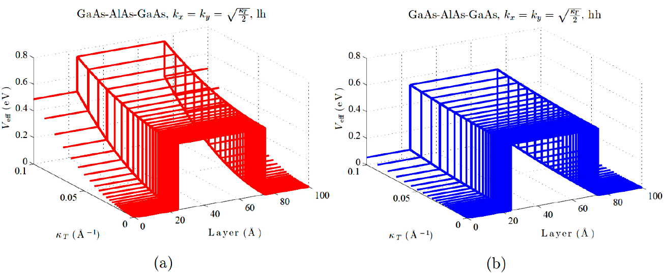
Figure 2 (Color online) Panel (a)/(b) displays the metamorphosis of the effective potential profile Veff for lh/hh (red/blue lines), as a function of κT and layer dimension for a GaAs/AlAs/GaAs heterostructure.
An appealing situation arises at a specific entry of the transverse momentum. An earlier
detailed study on this subject12 , has predicted the existence of quantity
being Vo = Veff(κT = 0) and A/B standing for concomitant cladding/middle layer. A direct consequence for Veff being flat at κTo is the existence of a crossover of Veff respect to (24).
In other words, if a QW-like profile is present for
In Fig. 3(a) the Veff valence-band mixing dependence, exhibits a neatly permutation of the Veff character as the one predicted for electrons12 . This permutation pattern is what we call “keyboard” effect, and was detected for lh only in stress-free systems. This striking interchange of roles for QB-like and QW-like layers, whenever the in-plane kinetic energy, varies from low to large intensity, represents the most striking contribution to the present study. For a single-band-electron Schrödinger problem, some authors have predicted that both QW and QB may appear in the embedded layers of a semiconductor superlattice, depending on the transverse-component value of the wave vector12 . It has recently been unambiguously demonstrated that the effective-band offset energy Veff, “felt” by the two flavors of holes, as κT grows, is not the same. Inspired by these earlier results, we have addressed a wider analysis of this appealing topic, displayed in Fig. 3, pursuing a more detailed insight. We have considered a InAs/AlSb/InAs heterostructure. Panel (a)/(b) of Fig. 3 shows explicitly the metamorphosis of Veff, felt by both flavors of holes independently, respect to concomitant-material slabs. From panels (a) and (b), it is straightforward to see that for hh (blue lines) an almost constant Veff remains, while κT varies from 0 (uncoupled holes) to 0.1 Å-1 (strong hole band mixing), despite the respective band-edge levels have changed. Contrary to hh [blue lines, panel (b)], the lh exclusively [red lines, panel (a)] exhibit the keyboard effect, i.e. they feel an effective band offset exchanging from a QW-like into a QB-like one, and viceversa for an InAs/AlSb/InAs heterostructure while κT increases. The evident keyboard effect of Veff, resembles a former prediction for electrons . This observation means that in the selected rank of parameters for a given binary-compound materials, a lh might “feel” a qualitative different Veff (QW or QB) during its passage through a layered system, while the degree of freedom varies in the transverse plane. Former assertions can be readily observed in Fig. 3(c)-(d), where we have plotted the evolution of Veff profile [panel (c)], as well as the progression of the band offset [panel (d)], with κT at a fixed transverse plane of the heterostructure. Both upper-edge and lower-edge move in opposite directions [see panel (c)] and the zero-band offset point configuration is detected in the vicinity of κT ≈ 0.066 Å-1 [see panel (d)]. The permutation holds for other in-plane directions, as can be seen from panel (c). Although not shown here for simplicity, the keyboard effect, remains robust for other middle-layer binary compounds, namely: AlAs, AlP, and AlN.
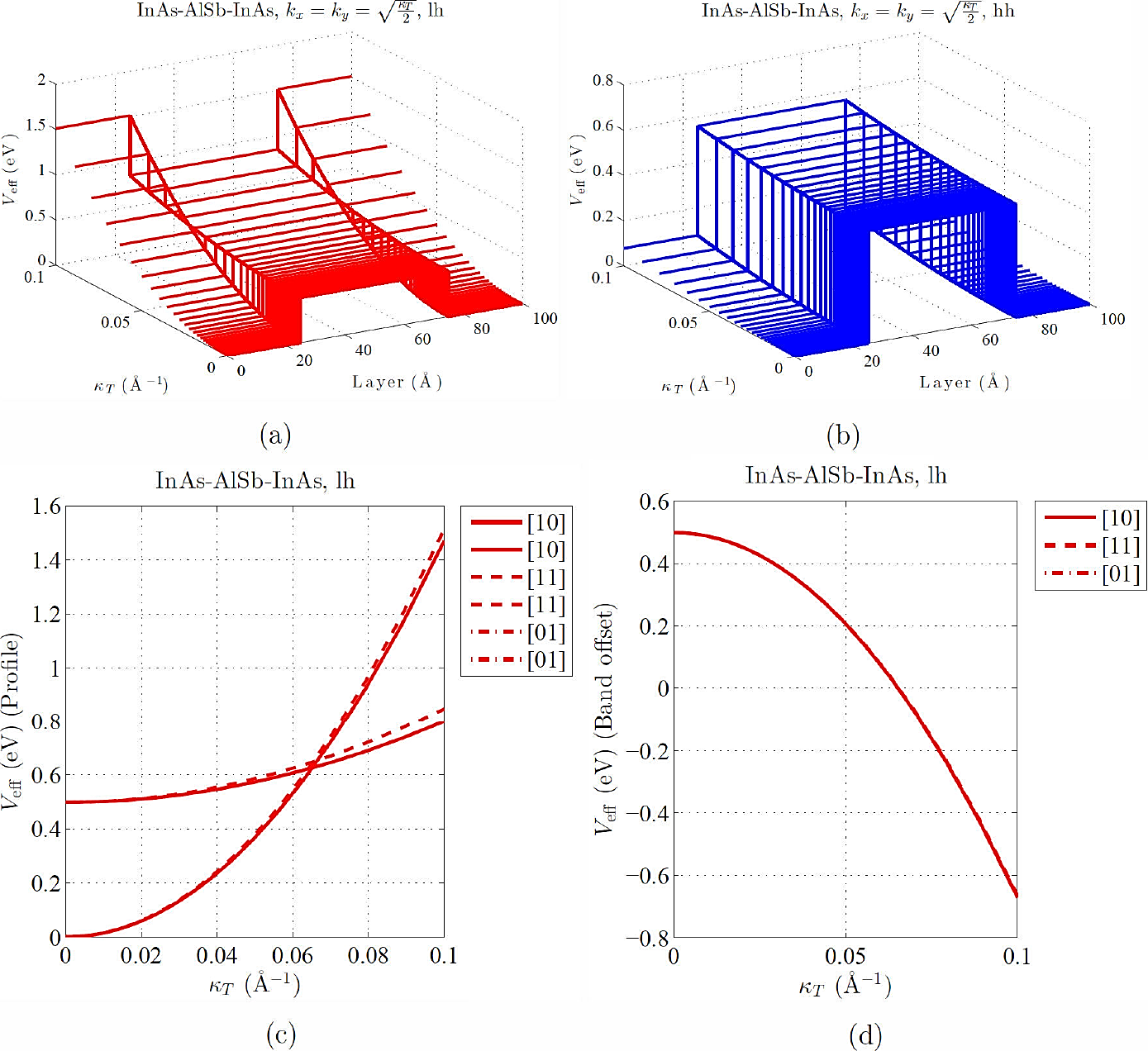
Figure 3 (Color online) Panel (a)/(b) displays the 3D-perspective evolution of the Veff profile for lh/hh (red/blue lines), as κ T and layer dimension grow. Panel (c) displays a cut of the Veff profile for lh (red line), at the interface plane between left and middle layers, as a function of κT. Panel (d) shows the progression of the band offset, at the same interface for lh, i.e. the difference between the upper-edge and lower-edge of the Veff profile. We have considered a InAs/AlSb/InAs stress-free layered heterostructure.
3.1.2. Keyboard effect versus pseudomorphic strain
Turning now to built-in elastic stressed layered heterostructures, we are interested in answering a simple question: whether or not the existence of a pseudomorphic strain becomes a weak or a strong competitor mechanism able to diminish the keyboard effect on Veff, or even make it rises/vanishes occasionally. Thereby, we need to account the accumulated strain energy resulting from the tensile or compressive stress acting on the crystal slabs. The last requires to solve ([for:Weff-s]), assuming the heterostructure sandwiched into a pseudomorphically strained QW/QB/QW-sequence.
Figure 4 is devoted to demonstrate that the keyboard pattern for lh remains robust in a InSb:InSb/AlN/InSb pseudomorphically strained layered heterostructure [see panel (b)], respect to that of the stress-free system [see panel (a)]. In this case, we conclude that maximized U s ([for:Strain]) do not represent any antagonist mechanism regarding to valence-band mixing influence on Veff. Identical middle-layer nitride material (AlN) may not follow a same evolution of VB-offset, if the concomitant cladding layers change. This in shown in panel (c), whose displayed behavior is the opposite to that in panel (a), i.e. we found no evidences of the keyboard effect. In this case, none zero-band offset point configuration were found even at strong VB mixing, though a remarkable anisotropy was detected, despite a common trend of Veff is neatly preserved. On the contrary, a robust isotropic character in the VB-offset progression for the same middle-layer binary compound embedded in the strained heterostructure, have been detected and shown in panel (d).
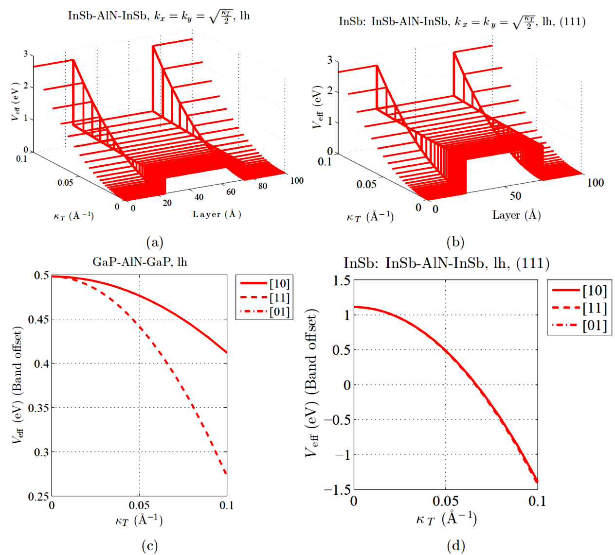
Figure 4 (Color online) Panel (a) displays the 3D-perspective evolution of the stress-free Veff profile for lh as κT and layer dimensión grow. Panel (b) shows the same for a InSb:InSb/AlN/InSb strained layered heterostructure. Panel (c) exhibits the evolution of the band offset for lh, in a stress-free GaP/AlN/GaP system. Panel (d) shows the same for a InSb:InSb/AlN/InSb strained heterostructure.
Figure 5(b) exhibits an unexpected keyboard effect for lh in a InP:GaP/AlSb/GaP layered heterostructure under a pseudomorphic strain, in comparison with a stress-free heterostructure [see panel (a)]. This evidence encourages to suggest Us ([for:Strain]) as a trigger mechanism in the presence of valence-band mixing to influence Veff, forcing a qualitative distinctive phenomenology to arise in the effective VB-offset profile (keyboard effect). Besides, it is worth to underline the inversion of the valence-band line-up, which is also remarkable considering the appealing interplay from QW-like to QB-like behavior (and viceversa) when comparing both stress-free [see panel (a)] and strained [see panel (b)] heterostructures. It is worth noticing the difference in the phenomenology of several stressed antimonide-based systems, respect to that discussed for nitride ones in Fig. 4(d). As can be seen in Fig. 5(c), an anisotropic pattern characterizes the lh case in a InP:GaP/AlSb/GaP layered heterostructure under a pseudomorphic strain. Importantly, the keyboard effect on Veff stays steady along [10] and [01] in-plane directions, while vanishes in the [11]. Thus a topological tuning of this striking effect reveals possible.
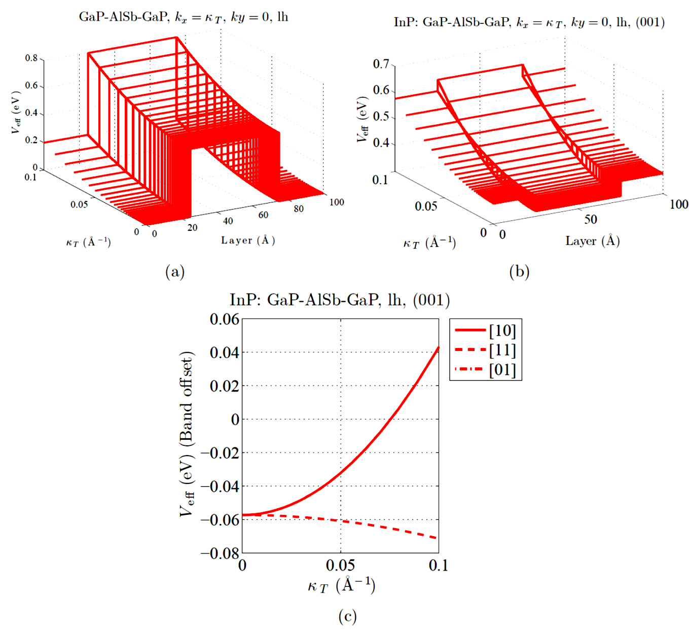
Figure 5 (Color online) Panel (a) displays the 3D-perspective evolution of the stress-free Veff profile for lh as κT and layer dimensión grow. Panel (b) shows the same for a InP:GaP/AlSb/GaP strained layered heterostructure. Panel (c) plots the progression of the band offset for lh, considering a InP:GaP/AlSb/GaP strained heterostructure along several in-plane directions.
Figure 6 shows another striking performance of Veff, when unexpectedly a keyboard effect has arisen for hh in a InSb:GaP/AlAs/GaP strained layered heterostructure [see panel (b)]. Indeed, if we consider the stress-free case of Fig. 6(a), we can see that the standard rectangular distribution for Veff remains consistent in a wide range of κT. Furthermore, a valence-band line-up inversion takes place, which is yet another remarkable performance for QW-like and QB-like slabs. For the sake of continue the qualitative insight into the influence of the concomitant cladding/middle layers as presented in the discussion of Fig. 4(a,c), we alter here just the cladding ones. At the opposite to the mentioned previous case for lh, the same kind of Veff evolution for hh remains [see panels (a) and (c)], however a difference of tendency along [10] and [01] in-plane directions, respect to that of the [11], was observed. We underline in panel (d), the possibility for topological tuning of the keyboard effect on Veff, as for hh now the [11] in-plane direction solely shows a zero-band offset point at the vicinity of κT ≈ 0.075 Å-1.
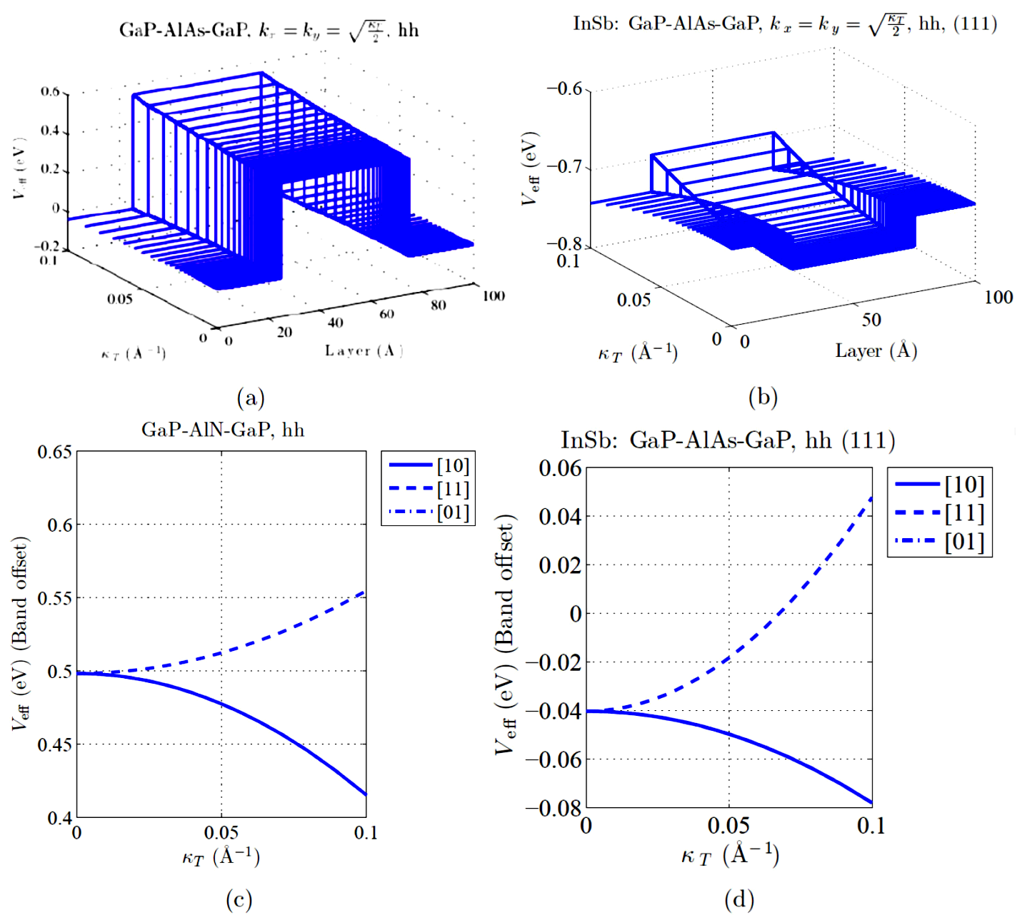
Figure 6 (Color online) Panel (a) shows the stress-free evolution of Veff for hh as a function of κT and layer thickness. Panel (b) shows the same for a AlN:GaP/AlAs/GaP strained layered heterostructure. Panel (c) displays the metamorphosis of the band offset for hh, in a stress-free GaP/AlN/GaP system. Panel (d) shows the same for a InSb:GaP/AlAs/GaP strained heterostructure.
Finally, Fig. 7 confirms the existence of a strong competitor mechanism between strain and keyboard effect. We can see in Fig. 7(b) how the keyboard pattern vanishes in a AlAs:InAs/AlN/InAs layered heterostructure under a pseudomorphic strain. The envisioned effect was apparently robust for the stress-free analogous systems shown in panel (a), within the selected range of κT. In panel (d), a resembling phenomenon was found for the strained InSb:InSb/AlAs/InSb layered heterostructure, with an appealing bonus of the interplay from QW-like to QB-like behavior (and viceversa) of the slabs. The last inversion of the valence-band line-up was not obtained for the stress-free correspondent system, exhibited in Fig. 7(c).
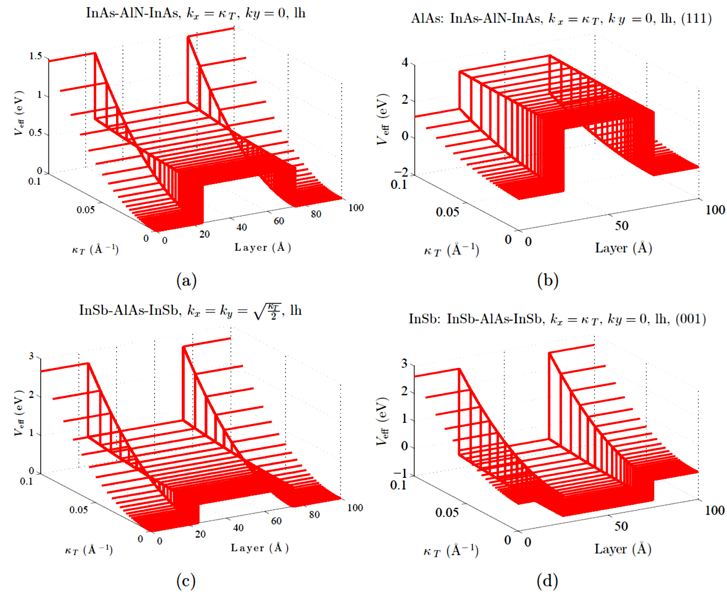
Figure 7 (Color online) Veff profile metamorphosis of for stress-free/strained layered heterostructure (panel a,c)/(panel b,d) as κT and layer thickness increase.
Although not depicted here, we have found qualitative patterns alike keyboard effect under pseudomorphic strain, for several III - V binary compounds (see Table I). As a bonus, a numerical evaluation of the polynomial interpolation (16) is presented in the last column of the Table I, thus complementing the characterization of the selected systems.

3.2 Influence of the pseudomorphic strain on kz -spectrum
The QEP kz-spectrum is a meaningful, and well-founded physical quantity that can be obtained via the root-locus-like procedure19 by unfolding back in the complex plane the dispersion-curve values for bulk materials, determined by stress-induced effects on the stress-free heterostructure. Thus, we take advantage of the root-locus-like know-how, to promptly identify evanescent modes, keeping in mind that complex (or pure imaginary) solutions are forbidden for some layers and represent unstable solutions underlying the lack of hospitality of these slabs for oscillating modes. The opposite examination is straightforward and also suitable for propagating modes, which become equated with stable solutions for given layers.
To obtain the QEP kz-spectrum in a periodic pseudomorphically
strained heterostructures of QB-acting/QW-acting/QB-acting materials, we first
use ([for:Weff-s]) and substitute it in
The Fig. 8 and 9
illustrate the role of band mixing for κT
[10-6, 10-1] Å-1, on the
kz spectrum from QEP (7) for a III-V strained
alloy, clearly distinguished as QW in most layered systems of technological
interest. Importantly, by assuming two different substrates AlSb (Fig. 8) and InAs (Fig. 9), we found different patterns of the
kz spectrum for lh and
hh. Namely for the [10] in-plane direction, the
kz
root-locus-like evolution is real for lh, in
the range of
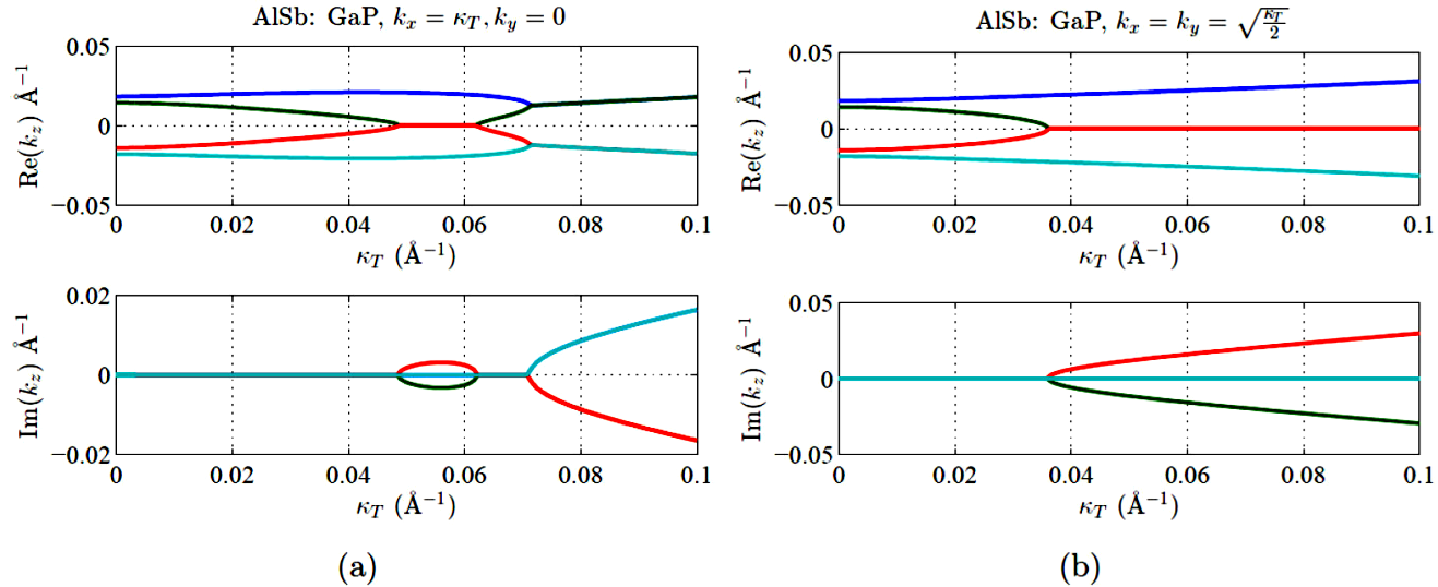
Figure 8 (Color online) Root locus for the eigenvalues kz from QEP (7), as a function of κT for strained AlSb(substrate)/GaP (epitaxial layer). We had assumed E = 0:6 eV, and in-plane directions [10]/[01] for panel (a)/(b).
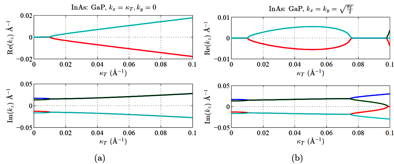
Figure 9 (Color online) Root locus for the eigenvalues kv from QEP (7), as a function of κT for strained InAs(substrate)/GaP (epitaxial layer). We had assumed E = 0:45 eV, and in-plane directions [10]/[01] for panel (a)/(b).
For completeness, the pseudomorphic perturbation on several stress-free hexagonal heterostructures have been considered here and we found slight modifications in the band offset compared to the unstrained case for growth planes (0001) and (1m00). However, nor permutations of Veff neither keyboard patterns were detected in such semiconductors materials.
3.3 Bandgap and valence-band offset manipulation
It has widely been accepted that electronic properties can be tuned by elastic stress. This assertion is clearly illustrated computationally for VB in Figs. 4, 5, 6 and 7, which exhibit modifications of the VB-offset whenever a biaxial-pseudomorphic strain is applied. Recently, some authors have addressed a first-principles density functional theory calculations to a monolayer of a MoS2 and indicate that both direct and indirect bandgap decrease in the presence of biaxial strain, with transitions from direct to indirect bandgap27. As uniform stress leads to band-structure changes, we thereby expect the bandgap of exercised III-V heterostructures displayed in Figs. 4, 5, 6 and 7, to evolve from nominal unstrained crystal spectrum forbidden gap. It is worth noting that as shown independently in Fig. 3(c,d), the way to tune the Veff profile as well as the VB offset is by letting grow the hh - lh coupling. The latter represents a complementary tool, to that proposed before27,28 in manipulating the electronic structure, but this time for tensile strain-free systems. Importantly, VB-offset progression depicted in Figs. 3(c,d), 5(b) and 6 for III-nitride(antimonide) heterostructure, as one of its constituent media, demonstrates an anisotropic behavior, as a bonus to the expected differences between hh and lh, due to their effective masses.
In Subsecs. (3.1.2) and (3.3) we have shown the Veff profile evolution and the keyboard effect under the competitors hole-mixing and strain. We hope that these appealing events would attract the attention of a wider community of physicists beyond condensed-matter theoreticians. The present graphic modelling of Veff evolution, may be a reliable workbench for testing several configurations of materials with minor changes, if any, being useful in both experimental applications and in theoretical analysis. The latter means that rather than considering the present study as an end-in-itself theoretical exercise -which is not ourgoal-, readers working in complementary and even in different fields most use (16) for zinc blende, and (22) for wurtzite to quote Veff eigenvalues from (9) and this way incorporate the mutable profile of Veff instead of the commonly used fixed V(z) = VB - VA. If the studies involve electronic properties and/or scattering processes, modifications of the conductance and thereby the tunneling time, should be expected by taking realistic Veff mutable quantities derived from work out the eigenvalue problem (9)-(10) rather than take a constant-guess value V(z) = Vo. We strongly recommend to include current results to further improve own researches that should be related to the real-world experiments and day-to-day applications.
4. Conclusions
We present an alternative graphic-based unambiguous theoretical procedure to demonstrate the VB-mixing and strain impact on Veff metamorphosis. Have been accurately derived an analytic expression of the VB-offset for zinc blende semiconductors, while for the wurtzite its explicit eigen-values were deduced from the proper (6 × 6) Hamiltonian . The lh experience the striking keyboard effect of Veff in stress-free and stressed systems. Nevertheless, in strained heterostructures the former behavior have been also found for hh. Evidences of this sort foretell their usefulness in experimental applications such as: VB-profile tuning, VB-offset manipulation and in theoretical analysis of hole tunneling and spectrum. Pseudomorphic strain is able to diminish the keyboard effect and also makes it emerge or even vanish eventually. We remark that the multiband-mixing and stress-induced events, are strong concurrent appliances that can not be universally neglected in layered systems. Tuning in-plane directions the keyboard effect under strain reveals anisotropic and thereof topologically tunable. The present modelling of V eff evolution, may be a reliable workbench for testing other configurations and may be of relevance for promising heterostructure’s design guided by VB-structure modelling to enhance the hole mobility in III-V semiconducting devices provided they always lagged compared to II-IV media 8.

