


 nueva página del texto (beta)
 Inglés (pdf)
 Artículo en XML
 Referencias del artículo
 Enviar artículo por email
 Citado por SciELO
  Similares en
SciELO
Similares en
SciELO 
 Permalink
PACS: 85.30.Tv; 85.30.De
1.Introduction
Currently, flexible and transparent electronics are of great interest, mainly, for the high potential to enable a wide variety of low-cost novel applications, such as, flexible displays, sensors and wearable electronic circuits 1-6. Many of these are possible by the development of thin-film transistors, where considerable improvements in organic, metal-oxide and chalcogenide based devices have been achieved 7,8,9,10. In this technology, solution-process techniques are attracting great attention due to the advantage over typical-used techniques, such as simplicity, compatibility with large-area substrates, low-cost and no-vacuum need. Although, solution-processed electronic devices have already been demonstrated, the fabrication temperature used in active and dielectric layers is high in order to obtain good performance devices11,12,13,14. Then, it is necessary reduce the fabrication temperature at values close to 200oC in order to be compatible with most of the low-cost flexible substrates.
In this work, we report the fabrication and characterization of MOS and MIM capacitors using a solution-processed dielectric based on spin-on glass (SOG) solution diluted with deionized water (DI). The SOG solution form an arrangement of silicate polymers with a Si-O structure, these polymers are in an alcohol solvent system. Here, the SOG solution is diluted with deionized water in order to make easier the evaporation of the organic material presented in the SOG solution, since the films are cured at lower temperature than the indicated by the producer 15. In previous work 15, it was demonstrated that dilution of SOG is necessary to obtain good quality films cured at temperatures below 300oC. The films produced from diluted-SOG solution showed a considerable reduction in the organic content compared with films produced from non-diluted solution. In order to demonstrate the application of the solution-processed SOG/DI films as dielectric for electronic devices, the films are cured at 200oC and 300oC, while the films cured at 470oC are used for comparison.
2. Experiment
The SOG solution (SOG700B Filmtronics) was diluted 3:1 with deionized water (DI) and spin coated into the samples. To fabricate the MOS and MIM capacitors, n-type silicon wafers (Phosphorous, 1-10
The capacitance-voltage and current-voltage characteristics were measured using the Keithley-4200 Semiconductor Characterization System equipped with the 4200-CVU Integrated C-V, under dark conditions, air ambient and room temperature. The characteristics here reported are representative of 8 capacitors in each set of devices.
3. Results and discussion
Figure 1 shows the optical transmittance for the SOG/DI films cured at 200oC, 300oC and 470oC. The films are highly transparent in the visible range, which makes feasible they use in transparent electronics. Although the spectra is similar for the three films, it can be seen the film cured at 200oC is slightly less transparent than the film cured at 470oC. This may be attributed to residuals in the SOG/DI films cured at lower temperature 15,16.
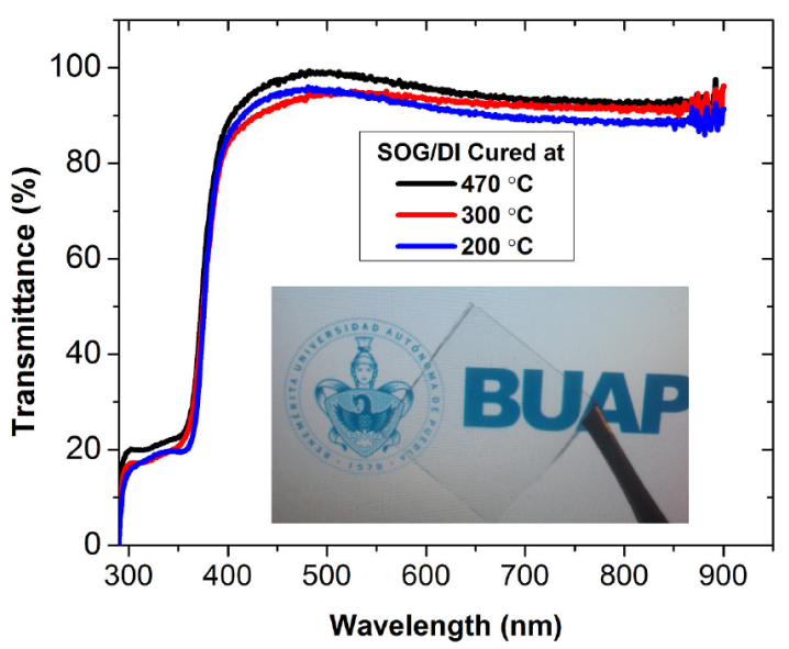
Figure 1 Optical transmittance of the SOG/DI thin films on glass slides at different deposition temperatures. Inset: SOG/DI thin film deposited at 200oC.
Figure 2 shows the capacitance-voltage characteristics at 50 KHz for the n-type MOS capacitors using the SOG/DI films cured at 200oC and 470oC for comparison. The characteristics of the three sets of capacitors show a well-defined accumulation region with low hysteresis, demonstrating the application of the SOG/DI films as gate dielectric for electronic devices. Despite on this, the MOS capacitors using the SOG/DI film cured at 470oC show slightly less hysteresis than the capacitors using the film cured at 200oC. This behaviour can be attributed to less organic residuals due to the higher curing temperature 15,16. From the overall capacitance-voltage characteristics, one can conclude that a high-quality dielectric-semiconductor interface is achieved regardless of the curing temperature.
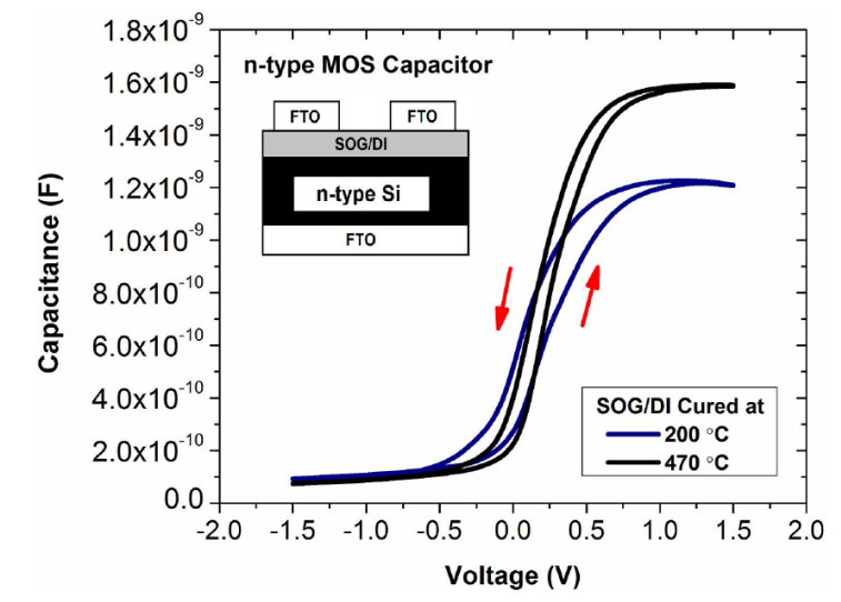
Figure 2 Capacitance-voltage curves of the n-type MOS capacitors using SOG/DI films at 470±C and 200oC. Inset: schematic cross section of the MOS capacitor.
Figure 3 shows the current density as function of the electric field from the MIM capacitors. All the MIM capacitors have similar values of current density and breakdown voltage. Although it was expected a higher breakdown voltage, the approximately 4 MV/cm obtained is reliable for applications of electronic devices 13,14. At 1 MV/cm, it can be observed, the MIM capacitors using the SOG/DI film cured at 470oC show less current density compared with the MIM capacitors cured at lower temperature. For higher electric fields than 1 MV/cm, the values of current density are similar until the dielectric breakdown. The behaviour of the electrical characteristics may be due to Pores induced by the evaporation of solvents during the curing of the film and to the curing ambient 13,16. Using Oxygen or Nitrogen ambient may improve the quality of the film 15,16.
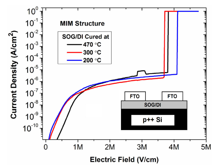
Figure 3 Current density as function of the electric field of the MIM structures. Inset: schematic cross section of the MIM structure.
On the other hand, it was proposed to show the dependence of the dielectric constant with frequency (Fig. 4). The n-type MOS capacitors using SOG/DI films cured at 470oC show a clear and unexpected dielectric constant dependency with frequency. Contrary to this, the MOS capacitors using SOG/DI films cured at 300oC and 200oC not shown a dependency at frequencies below 10 KHz but at higher frequencies. The later may be due to thermal stress in the films induced by the thermal shock from the initial 100oC to the immediate final curing temperature, where the films cured at 470oC are the most thermal stressed. One possible solution may be increasing the initial temperature by a slow ramp until the final curing temperature is reached, avoiding the thermal shock. Further research is necessary to address these assumptions.

Figure 4 Dielectric constant as function of the frequency of the SOG/DI thin films at different deposition temperatures.
From the results here reported, although the SOG/DI films are better in quality when they are cured at higher temperature, the films cured at 200oC and 300oC present high-quality dielectric properties and are compatible with glass substrates and some flexible substrates, which make feasible their use as gate dielectric for low-cost transparent thin-film Transistors.
4. Conclusions
In this work, the fabrication and characterization of MOS and MIM capacitors using a solution-processed dielectric based on spin-on glass solution diluted with deionized water is successfully presented. The films are highly transparent in the visible range. The C-V and I-V characteristics of the three sets of capacitors show a well-defined accumulation region with low hysteresis. A high-quality dielectric-semiconductor interface is achieved regardless of the curing temperature. The breakdown voltage of 4 MV/cm obtained is reliable for applications of electronic devices. Some unexpected characteristics may be due to a thermal stress in the films induced by a thermal shock and Pores induced by the evaporation of solvents, both of them, during the curing of the films.

