Research
Impact of planarized gate electrode in bottom-gate thin-film transistors
M.A. Domíngueza
P. Rosalesb
A. Torresb
F. Floresa
J.A. Lunaa
S. Alcantaraa
M. Morenob
aCentro de Investigaciones en Dispositivos Semiconductores, Instituto de Ciencias, Benemérita Universidad Autónoma de Puebla, Puebla, 72570, México. Tel/Fax: (52)(222) 229-55-00 Ext 7876 e-mail: madominguezj@gmail.com
bNational Institute for Astrophysics, Optics and Electronics, Electronics Department, Luis Enrique Erro No. 1, Puebla, 72840, México
Abstract
In this work, the fabrication of bottom-gate TFTs with unplanarized and planarized gate electrode are reported, as well simulations of the impact of the gate planarization in the TFTs are presented. Previously in literature, a reduction of the contact resistance has been attributed to this planarized structure. In order to provide a physical explanation of this improvement, the electrical performance of ambipolar a-SiGe:H TFTs with planarized gate electrode by Spin-On Glass is compared with unplanarized ambipolar a-SiGe:H TFTs. Then, the properties in the main device interfaces are analyzed by physically-based simulations. The planarized TFTs have better characteristics such as field-effect mobility, on-current, threshold voltage and on/off-current ratio which are consequence of the improved contact resistance.
Keywords: Thin-film transistor; hydrogenated amorphous silicon-germanium; simulation; planarization
PACS: 85.30.Tv; 85.30.De
1.Introduction
Thin-film Transistors (TFTs) are successfully employed in active-matrix displays, where considerable improvements in organic, oxide and chalcogenide TFTs have been achieved. However, the contact resistance is still a bottleneck due to the lack of a source/drain heavily doped interlayer film. Moreover, since the active-matrix displays become larger (where the inverted staggered structure is the most used), the number of address lines must increase and the gate lines must be longer and narrower. To avoid a delay in the display performance, the gate line must be thicker in order to reduce its resistance 1. Therefore, the problem associated with this thicker gate is that in the inverted staggered TFT structure the gate insulator tends to be thinner around the corners of the gate, causing that the insulator may suffer strong leakage and electric stress due to the high electric field at the corner 1,2. With the aim to reduce these effects, some groups have implemented a planarization process to planarize the gate electrode 2-6. J. Cheon et al. 3,4 used Spin-On Glass not only as gate dielectric but also to planarize the gate electrode. J. Lan et al. 5 reported a planarized Copper gate electrode for a-Si:H TFTs, while S. Martin et al., 6 reported planarized Organic Polymer TFTs.
As far as we know, in literature the only work related to the study of the planarization of the gate electrode is the reported by M. Chen et al. 2, where is reported a reduction in the contact resistance attributed by the planarization process. However, this improvement in the contact resistance is barely understood.
In this work, the fabrication of inverted staggered ambipolar a-SiGe:H TFTs with unplanarized and planarized gate electrode are reported, as well simulations of the impact of the gate planarization in the TFTs, in order to provide a physical explanation of the improvement in the contact resistance. The physical simulators ATHENA and ATLAS from Silvaco were used 7,8. Physically-based simulation has become very important for two reasons. One, it is much quicker and cheaper than performing experiments. Two, it provides information that is difficult or impossible to measure. The drawbacks of physically-based simulation are the rigorous knowledge of the relevant material parameters and device physics to be incorporated into the simulator, as well, numerical procedures must be implemented to solve the associated equations.
2. Experiment
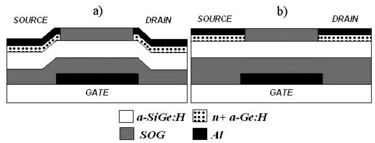
The devices were fabricated on Corning 1737 Glass substrate. The cross section of the planarized and unplanarized a-SiGe:H TFTs is shown in Fig. 1.
After planarize the gate electrode in one set, both set of devices were fabricated in the same process. To planarize the gate, 100 nm of silicon oxide (SiO2) by Spin-On Glass was deposited over the corning glass. Then, photoresist was applied and patterned to leave uncovered the place that will be used for the gate. Later, the SiO2 film was etching by Reactive Ion Etching leaving the place of the gate. Finally, the planarized gate is formed by lift-off and 100 nm of e-gun evaporated aluminum. 80 nm-thick of high quality SiO2 by Spin-On Glass was used as the gate dielectric for both devices. 100 nm-thick undoped a-SiGe:H and 40 nm-thick n-type a-Ge:H films were used as active layer and contact region film, respectively. 300 nm-thick aluminum e-beam evaporated as source and drain electrodes. The complete fabrication process can be found in Ref. 9.
The simulations were done as follows: using ATHENA, both unplanarized and planarized structures were generated following the fabrication process established. Si3 N4 was defined as the substrate, with no physical effects on the results.
The gate insulator used in the simulations was SiO2 with default properties values, because is the most similar to SiO 2 by Spin-On glass used in the a-SiGe:H TFTs 10). The parameters used for the a-SiGe:H and n-type a-Ge:H films were obtained from 11-15. It was used the TFT module to simulate the a-SiGe:H TFTs. Both electron and hole carriers were considered in the simulation. The temperature was set at 300 K. Newton’s method was the numerical method used for equations solution. The thickness used for the gate dielectric, a-SiGe:H and a-Ge:H films were 200 nm, 200 nm and 70 nm, respectively. The thickness of the source and drain electrodes, and passivation film are irrelevant for the simulation. The thickness of the gate electrode for planarized TFTs is also irrelevant for the simulation, while for unplanarized TFTs were 400 nm. After that, using ATLAS, a positive gate bias of 5 V (while Vds=0 V) was applied in order to study the effects of the planarization in the electric field around the corners of the gate. Finally, to analyze the TFTs interfaces (insulator-semiconductor and metal-semiconductor), one dimensional profiles were generated by the cutline tool 8,16.
3. Results and discussion
For the electrical characterization of the devices it was used a Semiconductor Parameter Analyzer (HP 4156B). All the measurements were performed in dark under ambient conditions.
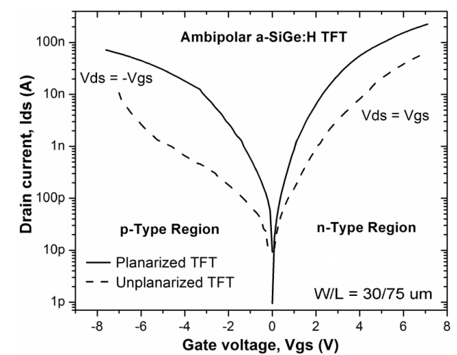
The measured transfer characteristic of unplanarized and planarized a-SiGe:H TFTs is shown in Fig. 2. The unplanarized a-SiGe:H TFT shows a subthreshold slope for n-type region and 1.3 V/DEC for p-type region, on/off-current ratios ∼104 and 103, for n-type and p-type regions respectively. Whereas the planarized a-SiGe:H TFT shows a subthreshold slope ∼0.45 V/DEC and ∼0.49V/DEC, for n-type and p-type regions respectively, while on/off-current ratios >105 and close to 105 for n-type and p-type regions, respectively. The threshold voltage and field-effect mobility were extracted from the transfer characteristics operating in the saturation regime ( Vds=Vgs). For unplanarized TFTs, the threshold voltage was 2.4 V for n-type region and -3.35 V for p-type region. The extracted field-effect mobilities were 0.11 cm2/Vs for n-type region and 0.02 cm2/Vs for p-type region. For planarized TFTs, the threshold voltage was 1.11 V for n-type region and -2.18 V for p-type region. The extracted field-effect mobilities were 0.68 cm2/Vs and 0.15 cm2/Vs for n-type and p-type regions, respectively.
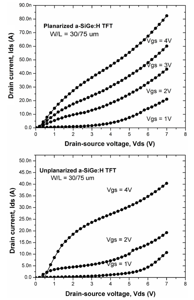
Figure 3 shows the output characteristics for planarized and unplanarized TFTs. The output characteristics show an ambipolar behavior, where the increase in the drain current (at higher values of Vds) is due to the contribution of the drain-induced holes. A detailed discussion and modeling can be found in Ref. 17. This ambipolar behavior has been also reported in nanocrystalline Silicon, Organic and Oxide semiconductors 18,19,20,21,22,23. Also, in the output characteristics of unplanarized TFTs a high contact resistance effect appears in the bias range of 0 to 1 V of Vds. This high contact resistance effect slightly appears in planarized TFTs. The values of drain current in planarized TFTs indicate their better driving current capability. Moreover, the contact resistance was extracted from the n-type region of both planarized and unplanarized ambipolar a-SiGe:H TFTs. A high contact resistance was confirmed by the extrapolation of the width-normalized contact resistance (RcW) (obtained from the linear region of Ids vs Vds) for different channel lengths and gate voltages Vgs. The RcW obtained was approximately 1413 Ωcm for unplanarized TFTs and 589 Ωcm for planarized devices. This high contact resistance reduces the on-current, the on/off-current ratio and masks the real value of the electron mobility. On the other hand, the subthreshold slope is improved in planarized TFTs by the reduced electric stress and better distribution of the electric field at the insulator-semiconductor interface, also, even by the improved contact resistance, since other authors have reported a better subthreshold slope by improving the contact resistance 24,25,26. Some published reports suggest that this may be due to a better injection of carriers from the source electrode into the semiconductor 26,27. All the above results are evidence of the performance improvement of the planarized TFTs and are in agreement with the reported by M. Chen et al. 2.
It is complex to understand why the planarization process, which affects the corners of the gate, will improve the metal-semiconductor interface (contact resistance). Considering that the electric field distribution around the corners of the gate is different for unplanarized and planarized TFTs, it is feasible that the higher electric field affect the contact regions (above the gate corners). In order to address this assumption, using ATHENA, both unplanarized and planarized structures were generated following the fabrication process established. After that, using the cutline tool within the ATLAS simulator, one dimensional profiles from the a-SiGe:H/ SiO2 and a-SiGe:H/n+ a-Ge:H interfaces were created. These simulations attempt to reproduce the impact of the planarized gate electrode comparing planarized and unplanarized simulated devices. Following this, although one can incorporate the extracted values of contact resistance into the simulator, this would force the simulation results. For this reason, the source/drain contacts in both planarized and unplanarized simulated TFTs were considered ideal contacts (without contact resistance).
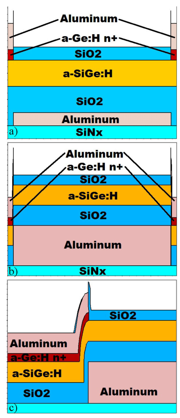
Figure 4 shows the cross section of planarized and unplanarized structures generated by ATHENA. Figure 4c shows a zoom at the corner of the gate of unplanarized TFTs, where the thinner gate insulator can be appreciated.
Figure 5 shows the electric field of the unplanarized and planarized structures extracted by ATLAS using the cutline tool, while a positive gate bias of 5V (at Vds=0 V) was applied. For the planarized structure, the electric field distribution is uniform through the insulator-semiconductor interface. While for the unplanarized structure, the electric field distribution is not uniform through the insulator-semiconductor interface. It can be seen that around the corners of the gate, just beneath of the metal-semiconductor interface, there is an increase of the electric field due to the thinner gate insulator. As expected, this higher electric field causes an increase in the electron concentration in the induced channel close to the corner of the gate, as show Fig. 6b. The difference of the electron concentration in the channel respect to that at the corner of the gate is more than one order of magnitude. These variations in the induced channel may act as a scattering mechanism, limiting the mobility of the carriers. This can explain the low on-current and, hence, the lower extracted field-effect mobility in the unplanarized TFTs. On the other hand, in Fig. 6a can be observed the uniform electron concentration through the channel for the planarized TFT.
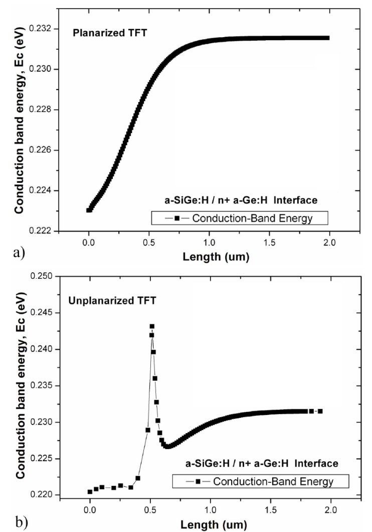
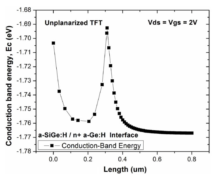
The variations of the electron concentration in the unplanarized TFT reflect an increase in the conduction band energy in the a-SiGe:H film at the a-SiGe:H/ n+ a-Ge:H interface, as show Fig. 7b. This increase in the conduction band energy acts as a barrier for the electrons, since only electrons with higher energy can pass above the barrier and be collected by the drain contact. Therefore, as result, the device contact resistance apparently increases. To corroborate this assumption, Fig. 8 shows the simulated conduction band energy in the drain contact of the unplanarized TFT at Vgs=Vds=2V, where the barrier can be appreciated. These can lead to an explanation of the high contact resistance effects appreciated at linear regime in the output characteristics of unplanarized TFTs and their lower drain current.
These results can be applied to other material based bottom-gate TFTs, even not ambipolar, since the parameters of the a-SiGe:H and a-Ge:H films are just responsible of the values extracted and do not affect the behavior here reported. It is important to mention that in real devices, the discussed effects may be higher because the gate insulator is even thinner than that presented in the simulations.
4. Conclusions
The planarized TFTs have better performance such as field-effect mobility, off-current, subthreshold slope, threshold voltage and on/off-current ratio which are due mainly to the improved contact resistance, the reduced electric stress and better distribution of the electric field at the insulator-semiconductor interface. It can be seen that around the corners of the gate, just beneath of the metal-semiconductor interface, there is an increase of the electric field. This causes an increase in the conduction band energy in the a-SiGe:H film at the a-SiGe:H/ n+ a-Ge:H interface. Therefore, this increase in the conduction band energy acts as a barrier for the electrons, resulting in the apparent increase of contact resistance.
Acknowledgments
The authors want to thank to all personnel of the Laboratory of Microelectronics at INAOE and to the CONACyT-Mexico for partial funding.
References
1. J. Kanicki and S. Martin, “Hydrogenated amorphous Silicon thin-film transistors”, in Thin Film Transistors, ed. by C. Kagan and P. Andry, Marcel Dekker Inc., (2003).
[ Links ]
2. M. Chen, J. Chou and S. Lee, IEEE Trans. Electron Devices 42 (1995) 1918.
[ Links ]
3. J. Cheon, J. Bae, W. Lee and J. Jang, Electrochem. Solid-State Lett. 11 (2008) H77.
[ Links ]
4. J. Cheon, J. Bae and J. Jang, IEEE Electron Device Lett. 29 (2008) 235.
[ Links ]
5. J. Lan and J. Kanicki, IEEE Electron Device Lett. 20 (1999) 129.
[ Links ]
6. S. Martin, J. Nahm and J. Kanicki, J. Electron Mater. 31 (2002) 512.
[ Links ]
7. ATHENA User’s manual, Silvaco International (2002).
[ Links ]
8. ATLAS User’s manual, Silvaco International (2002).
[ Links ]
9. M. Dominguez, P. Rosales, A. Torres and M. Moreno, Mater. Res. Soc. Symp. Proc. 1426 (2012) A19-03.
[ Links ]
10. M. Dominguez, P. Rosales, A. Torres, M. Moreno and A. Orduña, Thin Solid Films 520 2012 5018.
[ Links ]
11. P. Rosales, A. Torres, R. Murphy and M. Landa, Semiconductor Sci. Technol. 19 (2004) 366.
[ Links ]
12. P. Rosales et al., J. Appl. Phys. 97 (2005) 083710-1.
[ Links ]
13. M. Dominguez et al., J. Non-Cryst. Solids 358 (2012) 2340.
[ Links ]
14. M. Dominguez, P. Rosales and A. Torres, Rev. Mex. Fis. 59 (2013) 62.
[ Links ]
15. M. Dominguez et al., Thin Solid Films 562 (2014) 260.
[ Links ]
16. VWF Interactive Tools, Silvaco International (2004).
[ Links ]
17. M. Dominguez et al., Solid State Electron. 99 (2014) 45.
[ Links ]
18. K. Nomura, T. Kamiya and H. Hosono, Adv. Mater 23 (2011) 3431.
[ Links ]
19. A. Subramaniam, K. Cantley, H. Stiegler, R. Chapman and E. Vogel, IEEE Trans. Electron. Devices 59 (2012) 359.
[ Links ]
20. C. Lee, A. Sazonov, M. Rad, G. Chaji and A. Nathan, Mater. Res. Soc. Symp. Proc. 910 (2006) A22-05.
[ Links ]
21. C. Yang et al., Organic Electronics 12 (2011) 411.
[ Links ]
22. R. Ye, M. Baba, K. Suzuki and K. Mori, Solid State Electronics 52 (2008) 60.
[ Links ]
23. J. Zaumseil and H. Sirringhaus, Chem. Rev. 107 (2007) 1296.
[ Links ]
24. D. Han, Y. Kang, J. Park, H. Jeon and J. Park, Mater. Res. Bull. 58 (2014) 174.
[ Links ]
25. J. Wu, H. Lin, B. Su, Y. Chen, S. Chu, S. Liu, C. Chang and C. Wu, J. Alloys Comp. 592 (2014) 35.
[ Links ]
26. F. Chen, Y. Lin, T. Chen and L. Kung, Electrochem. Solid-State Lett. 10 (2007) H186.
[ Links ]
27. O. Marinov, M. Deen and B. Iñiguez, J. Vac. Sci. Technol. B 24 (2006) 1728.
[ Links ]


 nueva página del texto (beta)
 Inglés (pdf)
 Artículo en XML
 Referencias del artículo
 Enviar artículo por email
 Citado por SciELO
  Similares en
SciELO
Similares en
SciELO 
 Permalink