Research
GaN nanowires and nanotubes growth by chemical vapor deposition method at different NH3 flow rate
Pengan Li1
Yihe Liu1
Xianquan Meng1
1Key Laboratory of Artificial Micro-and Nanostructures Ministry of Education and School of Physics and Technology, Wuhan University, Wuhan 430072, Hubei, People’s Republic of China.
Abstract
GaN nanowires and nanotubes have been successfully synthesized via the simple chemical vapor deposition method. NH3 flow rate was found to be a crucial factor in the synthesis of different type of GaN which affects the shape and the diameter of generated GaN nanostructures. X-ray diffraction confirms that GaN nanowires grown on Si(111) substrate under 900o C and with NH3 flow rate of 50 sccm presents the preferred orientation growth in the (002) direction. It is beneficial to the growth of nanostructure through catalyst annealing. Transmission electron microscopy and scanning electron microscopy were used to measure the size and structures of the samples.
Keywords: GaN; CVD; nanotube; TEM
PACS: 81.15.Gh; 68.37.Lp; 81.07.De
1. Introduction
Gallium nitride (GaN), an important semiconductor with a band-gap of 3.4 eV, has high saturated electron drift velocity and high thermal conductivity 1,2. GaN nanostructures, for example, nanowires, nanorods and nanotubes have a bright application prospect in UV detector, high-temperature electronic devices, high-speed field-effect transistors, lasers, LEDs and other functional devices 3,4.
The GaN nanowires are very interesting building blocks for the fabrication of various nanoscale devices because of their own superior properties such as the capability of the doping modulation and the selectivity of the carriers3,5,6,7. GaN nanotubes can be obtained through two-step template-assisted methods and direct reaction of metal gallium with flowing NH 3 . However, the synthesis of high-purity well-structured GaN nanotubes is still a challenge,the mechanical properties of well-crystallized GaN nanotubes are still unknown due to synthetic difficulties8. In addition, it is essential to study the Young’s modulus of GaN nanotubes, which differ from GaN nanowires in shape, size, morphology and atomic structure, in order to fully evaluate their possibilities for nanoelectronic mechanical system (NEMS) devices1,9,10.
Liu et al. 1,11,12 have introduced a complex methord to synthesis the GaN nanotubes with mixed powder of Ga 2 O 3 and GaN.He et al. [13] gave the simple synthesis method of CVD,but they did not explore the mechanism.In this paper,we further discussed the influence of different NH 3 flow rate on GaN nanowires and nanotubes.
2. Experimental details
In this letter, GaN nanowires and nanotubes were synthesized through direct reaction of metal gallium (Ga,99.99%) vapor with flowing NH3 in a electric furnace. The Si (111) substrate was cleaned by acetone, ethanol, and de-ionized water with ultrasonic bath for 5 min each to remove residual organic contaminations on the surface. Three samples were synthesized at different ammonia concentration using nickel (Ni, ∼ 10 nm thick) as a catalyst. The Ga was placed on an quartz boat at the center of the furnace, and the Ni/Si (111) substrates was located about 1 cm downstream to the Ga source. The tube was pumped and filled with N2 for 3 times to clear the residual O2, then was gradually heated to 950oC at a rate of 25oC/min and kept for 10 min for catalyst annealing, protected by N2. The temperature was dropped to 900oC, the tube was bumped, NH3 was introduced at a desired flow rate. The first sample was grown using a NH3 flow rate of 50 sccm for 0.5 h, the second grown using a NH3 flow of 100 sccm for 0.5 h and the third grown using a NH3 flow of 200 sccm for 0.5 h.The growth temperature was maintained for a desired time. Finally the system was cooled down to room temperature in vacuum. GaN products were obtained on the Si (111) substrate.
3. Results and discussion
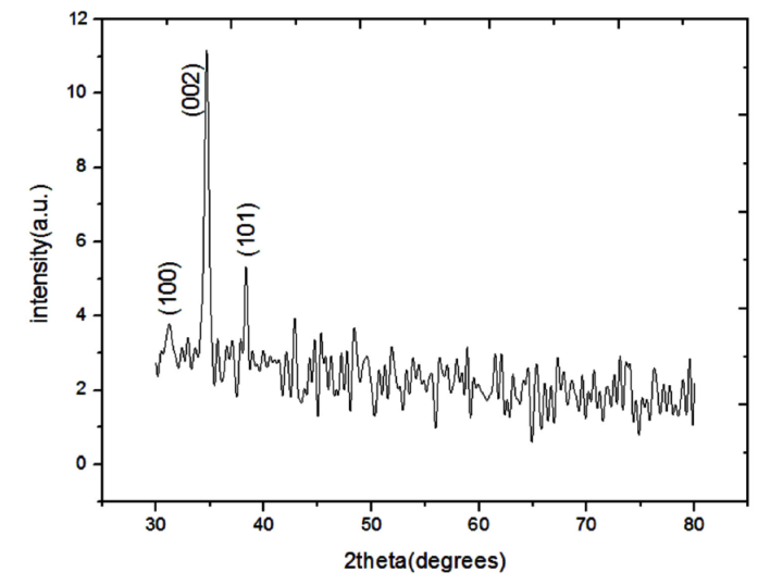
The first sample grown at 900oC with NH3 flow of 50 sccm is characterized by XRD. Figure 1 shows the XRD patterns of the GaN nanowires and the diffraction peaks show that the GaN nanowires present the preferred growth orientation on the (002) direction and good quality. Because of the lowest surface energy in the (002) crystal plane, the growth of GaN nanostructure tend to (002) crystallographic orientation, while the growth of other direction is subdued.
Before the growth of GaN nanostructures, the catalyst of nickel thin film must be annealed to transform it to nanoparticles. Substrate with nickel was gradually heated to 950oC at a rate of 25oC/min and kept for 10 min, then the temperature was dropped to 900oC with 5 min. The whole annealing process was under the protect of N2. Figure 2 (a) is the SEM image of not annealed nickel, and Fig. 2 (b) is the annealed one. It can be clearly seen from the images that catalyst become more compact and the sizes of catalyst particles are about 70 nm after anneal. So catalyst annealing is beneficial to the growth of nanostructure if we want better product.
Figure 3 shows the SEM images of GaN products, the SEM images (a) and (b) recorded the information of the first sample with GaN nanowires of diameters between 50 and 92 nm, most of the length can reach 5 μm. The images (c) and (d) come from the second sample, the product is much shorter than the first sample, but it has larger diameter in the range from 134 nm to 230 nm. From images (e) and (f), we can measure the diameter of the third sample range from 132 nm to 267 nm. At the same time, it is clearly seen that some nanosheets appear in Fig. 3 (e) and (f). Figure 3 (g) is the SEM image of Ni catalyst on the tip of GaN nanowire, this is typical evidence for VLS mechanism.
Figure 4 (a) is a TEM image of the first sample (nanowires), and the inset in the upper-left-hand corner of Fig. 4(a) is a selected area electron diffraction pattern (SAED) of the wire sample. Diameters of most of the wires can reach at 54 nm. Similarly, Fig. 4 (c) is the TEM image of the third sample. To our surprise, the one dimensional nanostructures in the third sample are GaN nanotubes. The inset picture of Fig. 4 (c) is an electron diffraction pattern of the nanotube. From the Fig. 4 (c), the outside diameter of the tube can up to 250 nm and an inside diameter of 160 nm. As mention above, some nanosheets appear in the third sample, Fig. 4 (b) is the TEM image of the third sample. We all know that the nanosheets would become the nanotube if they were rolled up properly.
Generally, under the same growth temperature, the faster the NH3 flow rate between 50 and 200 sccm, the larger the nanowires or nanotubes diameter. By the simple methord, GaN nanostructures with manifold morphologies, including nanowires, nanorodes,nanotubes and nanosheets are fabricated. NH3 flow has great impact on the morphology of the nanostructures. When the flow rate of NH3 is low, GaN nanowires are synthesized based on the VLS mechanism11. We get nanowires.As the flow rate increased,on the basis of VLS mechanism, the increase of the NH3 flow rate enhance the lateral growth, which leads to the decreasing of the length to diameter ratio and promoting the formation of nanorods and nanosheets. To date, the direct fabrication of a hexagonal GaN tubular structure free from contamination has been a challenge 12, the nanosheets as showed in Fig. 4(b) were transformed to the nanotubes by rolled up. The work may helpful to achieve the controllable fabrication of GaN nanostructures with varous morphologies.
4. Conclusions
In summary, with different NH3 flow rate between 50 and 200 sccm, large scale GaN nanowires and tubes were formed at the growth temperature of 900oC on Si(111) substrate. The GaN nanowires grown on Si(111) substrate under 900oC and with NH3 flow rate of 50 sccm present the preferred orientation growth on the (002) direction. When the NH3 flow rate increases to 100 sccm, the products have much wider diameter but shorter length. Continue to increase the NH3 flow rate to 200 sccm, we get nanotubes and nanosheets. This may be because the faster the NH3 flow rate, the greater the tension of the GaN surface. This leads to very easy to form nanosheets. As the temperature is reduced,nanosheets would become the nanotube if they were rolled up properly. We are continuing to study other factors which may influence the growth of GaN nanostructures, such as sample location, pressure and trying to gain an better understanding of the detailed growth mechanism.
Acknowledgments
This work was supported by the National Natural Science Foundation of China under Grant Nos. 11275144 and J1210061.
References
1. B.D. Liu, Y. Bando, M.S. Wang, C.C. Tang, M. Mitome and D. Golberg, Nanotechnology 20 (2009) 185705.
[ Links ]
2. K.M.A. Saron, M.R. Hashim, Materials Science and Engineering B 178 (2013) 330.
[ Links ]
3. T.H. Kim, S.Y. Lee, N.K. Cho, H.K. Seong, H.J. Choi, S.W. Jung and S.K. Lee, Nanotechnology 17 (2006) 3394.
[ Links ]
4. B.D. Liu et al., ACS Appl. Mater. Interfaces 6 (2014) 14159.
[ Links ]
5. H.F. Ji, M. Kuball, R.A. Burke and J.M. Redwing, Nanotechnology 18 (2007) 445704.
[ Links ]
6. G. Guzman and M. Herrera, Semiconductor science and technology 29 (2014) 025001.
[ Links ]
7. Q.N. Abdullah et al., Ceramics International 40 (2014) 9563.
[ Links ]
8. M.P. Persson and A.D. Carlo, Journal of Applied Physics 104 (2008) 073718.
[ Links ]
9. Y.J. Hong, J.M. Jeon, M. Kim, S.R. Jeon, K.H. Park and G.C. Yi, New Journal of Physics 11 (2009) 125021.
[ Links ]
10. Z.W. Liang et al., Journal of Applied Physics 108 (2010) 074313.
[ Links ]
11. B.D. Liu, Y. Bando, C.C. Tang, F. F. Xu, and D. Golberg, Appl. Phys. Lett. 87 (2005) 073106.
[ Links ]
12. B. D. Liu, Y. Bando, C. C. Tang, G. Z. Shen, D. Golberg, and F. F. Xu, Appl. Phys. Lett. 88 (2006) 093120.
[ Links ]
13. M. Q. He et al., Appl. Phys. Lett. 77 (2000) 3731.
[ Links ]


 nueva página del texto (beta)
 Inglés (pdf)
 Artículo en XML
 Referencias del artículo
 Enviar artículo por email
 Citado por SciELO
  Similares en
SciELO
Similares en
SciELO 
 Permalink