


 nueva página del texto (beta)
 Inglés (pdf)
 Artículo en XML
 Referencias del artículo
 Enviar artículo por email
 Citado por SciELO
  Similares en
SciELO
Similares en
SciELO 
 Permalink
1. Introduction
Planar waveguides with thickness smaller than the wavelength of the transmitted light have been recently proposed as promising components for nano-photonic devices. In these sub-wavelength thick planar waveguides, only a few discrete modes of light can be propagated [1]. High-speed and high-capacity optical connections are expected to be possible with optical sub-wavelength wave guiding [2].
Recently, the energy propagation in a planar waveguide was studied, with the transmitted and reflected energies estimated as a function of a discontinuity gap [3]; in that work, the authors compared some numerical methods in three different configurations. With the rapid development of photonic integrated circuits, it is convenient to revisit the discontinuity problem from the standpoint of mode conversion, which shall allow for more precise control of the flow of light. In recent years, there has been a lot of interest in the conversion of discrete modes in photonic waveguides due to its multiple applications [2, 4-6]. A mode converter relies on the waveguide propagation of the allowed modes. It produces a spatial spectrum of modes which relates the eigenmodes of the system. It is therefore desirable to design a dependable tool for switching from one spatial mode to another.
Several structures have been reported that enable conversion between the transverse electric fundamental mode (TE0) and the first higher-order mode (TE1) [7-11]. Mode conversion between two waveguides is obtained when these are connected together with a specific geometry that allows for mode change. For instance, it has been already investigated how to optimize the topology of a photonic crystal in order to achieve mode conversion due to interference processes [7, 8]. Another method of connecting two waveguides together consists in using a cavity as a mode converter [10]. The mode conversion across a bent waveguide has also been taken into consideration [11]; in that work, the mode conversion in a planar waveguide as a function of the bending angle was proposed. Sub-strip waveguides have also been investigated and manufactured as mode converters with variations in their topologies, using different silicon-based dielectrics, to convert the fundamental mode TE0 into the higher-order modes TE1 and TE2 [12].
While a planar waveguide is typically used as a simple connection between two components of an optical circuit, our research has uncovered an unexpected phenomenon. Specifically, we have observed that the introduction of a discontinuity in the planar waveguide leads to the excitation of higher-order modes. This finding highlights the potential for planar waveguides to serve as more than just a basic connection in optical circuits and suggests exciting possibilities for the development of novel devices and applications.
In an effort to answer the question that some authors have raised, of how to obtain the smallest possible mode converter [13], the present work is devoted to describe the simplest mode converter ever reported in a waveguide. Taking one of the three structures shown in [3] as the starting point, our mode converter is a dielectric planar waveguide with a step discontinuity that allows the mode TE0 to be converted into the higher order modes TE1 and TE2. We believe that this configuration could be easily modified to create a wide variety of compact photonic integrated circuits.
2. Theory
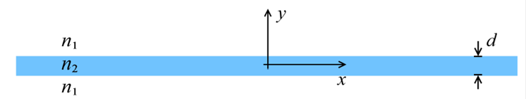
We start by considering a planar dielectric waveguide that consists of an infinite slab of width d. It has a refractive index n 2 = 3.6 and it is surrounded by air (n 1 = 1), as shown in Fig. 1. For the transverse electric polarization (TE), the electric field parallel to the z-axis can be expressed as
For a dielectric waveguide, the electromagnetic waves propagate inside the slab and vanish outside it.
The even and odd modes in a waveguide are given by two well-known transcendental equations [14]. The even-parity modes, related to the y-axis, are given by the equation
while the odd-parity modes are given by
where the reduced wave vectors are
The reduced frequency is written as
and the reduced wave vector, on the x-axis, is
The dispersion relations for the even and odd modes are shown in Fig. 2. The allowed modes exist between the light lines L
1 = n
1Ω and L
2 = n
2Ω (gray dashed lines), corresponding to the air and the dielectric, respectively. At the reduced frequency Ω = 0.32 (green line), only 3 guided modes are allowed: TE0, TE1, and TE2, which exist at the reduced wave vector values
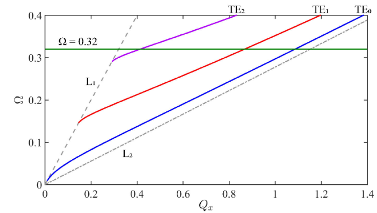
Figure 2 Dispersion relation for a planar waveguide. The gray dashed lines are the light lines for air (L1) and the dielectric material (L2). The guided modes are depicted with continue lines: TE0 (blue), TE1 (red), and TE2 (purple). The green continuous line indicates the reduced frequency Ω = 0.32.
3. Numerical method
The propagation of the electromagnetic field is simulated using the finite-difference time-domain (FDTD) method [15]. This computational technique is used to model the temporal evolution of Maxwell’s equations, based on the reformulation of the differential equations in central finite differences. In the case of time-dependent Maxwell’s equations, these are discretized by an approximation to spatio-temporal partial derivatives. The resulting system is written as a recursive computational algorithm, which can be solved in the time domain. In this work, we have performed the simulations of the FDTD method by implementing the Meep package, a freely available software [16].
Considering the polarization of the electric field along the z-axis, described in Eq. (1), we can rewrite Ampère-Maxwell’s equation as
whereas for Faraday’s equation, we have
Equations (7) to (9) can be reformulated in terms of central finite differences. For Eq. (7), considering a discretization at around
Now, considering the change for the point
Finally, by rewriting Eq. (9) in terms of finite differences at the point
To suppress spurious reflections of waves radiated from the artificial boundaries, perfect matched layers (PMLs) with a thickness of d, were implemented [16].
To validate the excitation of the guided modes, the Fourier transform (FT) of the electric field was implemented through the expression
where p 1 and p 2 are the discrete limits of integration such that the discontinuities in the waveguides near the origin and the PMLs are avoided.
4. Mode Conversion
To produce the simplest mode converter reported so far, to the best of our knowledge, we have considered a planar waveguide with two kinds of anisotropies: first, a discontinuity along the propagation axis (x-axis), and second, a lateral shift (y-axis). To simulate the propagation of light in the waveguide, a continuous and monochromatic light source was defined with a reduced frequency Ω = 0.32. According to Eq. (5), the wavelength of the source is
4.1. Horizontal shifting
We shall first analyze the mode conversion caused by a simple discontinuity gap of length L in the propagation direction of the waveguide, as illustrated in Fig. 3. This setup is similar to the one described in Fig. 8a), presented in Ref. [3] in section B. It is worth mentioning that, in contrast to the methodology employed by the authors, we successfully replicated the results of those sections A and B (Figs. 5 and 7 in Ref. [3]) using the FDTD method. Section C was not examined.
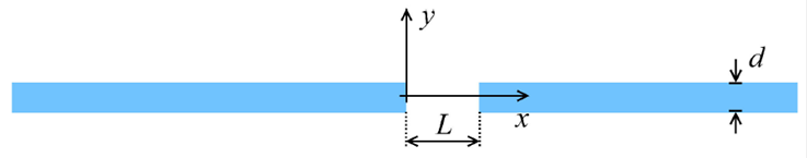
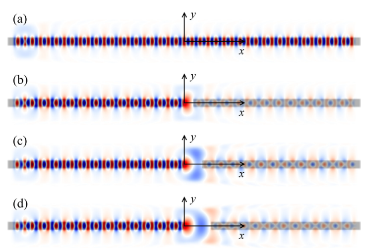
Figure 4 Propagation of the electric field, in the horizontal-shift converter (TE0 and TE2 modes), for the cases (a) L = 0, (b) L = d, (c) L = 2d, and (d) L = 3d.
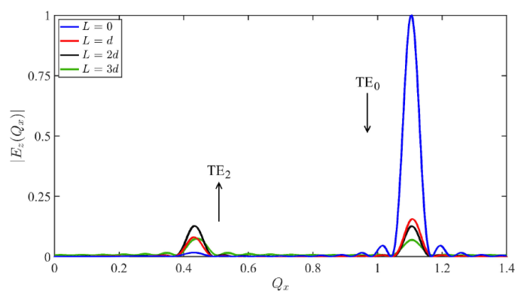
Figure 5 Fourier transform of the electric field for the horizontal shift: L = 0 (blue), L = d (red), L = 2d (black), and L = 3d (green).
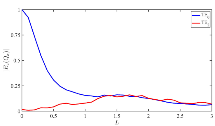
Figure 6 Evolution of the Fourier transform of the electric field as a function of the horizontal shift L. The intensity of the even modes TE0 and TE2 are represented by the blue and red lines, respectively.
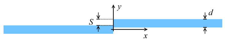
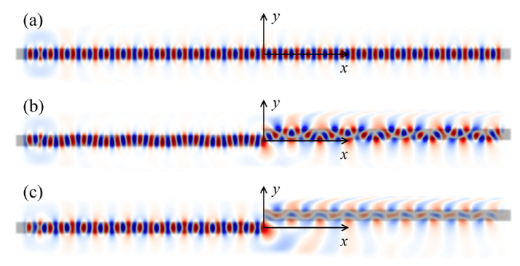
Figure 8 Propagation of the electric field, in the vertical-shift converter (from TE0 to TE1 and TE2 modes), for the cases (a) S = 0, (b) S = 0.5d, and (c) S = d.
The discontinuity length was taken from L = 0 up to L = 3d, as depicted in Fig. 4, where the spatial evolution of the electric field is shown for some cases. In Fig. 4a) (no discontinuity) the propagation of the fundamental mode is observed, while in Fig. 4b)-4d), the linear combination of the TE0 and TE2 modes is attested by those small lobes in the spatial profile in the guided mode. In all cases, symmetrical profiles with respect to the propagation axis can be observed because of the sole presence of even modes.
As light propagates through the original waveguide without discontinuities (L = 0), the fundamental mode TE0 is predominant as expected (Fig. 5; blue line). By implementing the FT through Eq. (13), we can clearly see that as the discontinuity gap L increases, the Fourier component of the modes varies, as illustrated in Fig. 5, for the values L = 0, d, 2d, and 3d. We have found that a simple horizontal discontinuity in the waveguide can induce high-order mode conversion from the TE0 to TE2, skipping the TE1 odd mode (no peak at
4.2. Lateral shifting
Considering a second configuration, whose geometry is presented in Fig. 7, we obtain a distinct mode converter. In this case, a lateral shift S is defined in the range from S = 0 (the original waveguide) to S = d. Figure 8 shows the lateral displacement for the cases when S = 0, S = 0.5d, and S = d, where the spatial evolution of the electric field is illustrated.
In Fig. 8a), the spatial profile of the propagated fundamental mode is presented again; in Fig. 8b), an asymmetrical profile is observed due to the presence of the TE1 odd mode, in a linear combination with the TE0 and TE2 modes. Finally, Fig. 8c) shows a symmetrical spatial profile due to the presence of the TE2 mode only since there is no contribution of the other modes
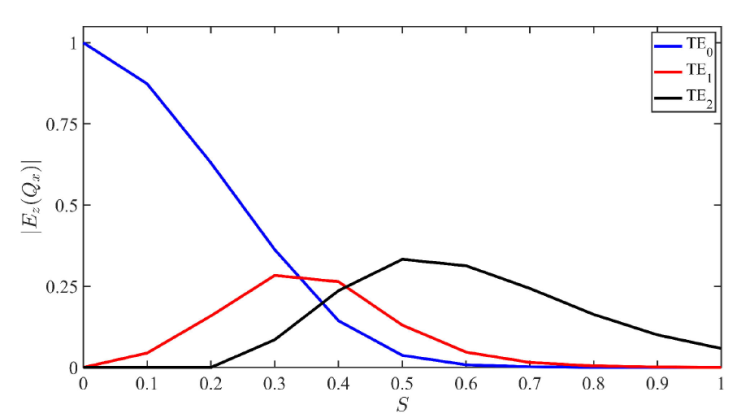
As presented in Fig. 9, by increasing the shifting S, a conversion from the TE0 mode to the higher-order modes TE1 and TE2 is induced. Here it can be seen that, for values greater than 0.6d (Fig. 9; black line), the TE0 and TE1 modes have almost no contribution. In fact, Fig. 10 shows the evolution of the FT in the range from S = 0 to d. When the lateral shift S is about 0.7d, the fundamental mode becomes negligible; likewise, when S = 0.8d, the TE1 mode is practically extinguished. In the figure it can also be seen that the maximum for the TE1 mode is around 0.35d, and around 0.55d for the TE2 mode. We have found that after S = 0.8d, only the TE2 mode propagates.
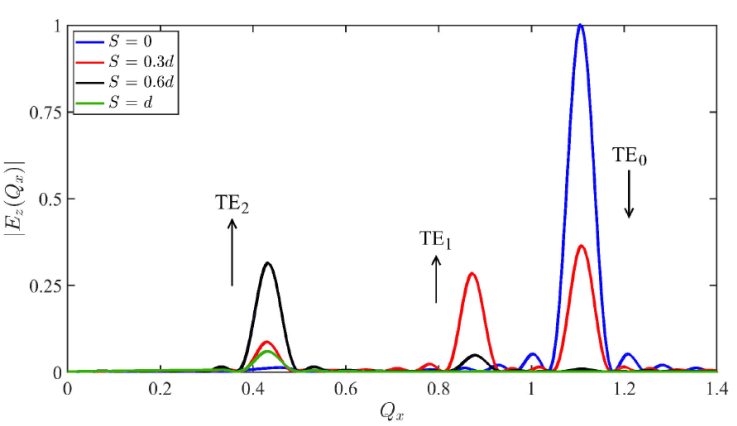
Figure 9 Fourier transform of the electric field for the lateral shift: S = 0 (blue), S = 0.3d (red), S = 0.6d (yellow), and S = d (green).
5. Conclusion
The most basic high-order waveguide mode converter induced by discontinuities is proposed here. On the one hand, by allowing a simple discontinuity in the propagation axis of the waveguide we created a mode converter. We found that the TE0 and TE2 modes are excited in this setup and the TE1 odd mode is skipped and consequently not excited. On the other hand, the fundamental mode TE0 can be converted into the higher-order modes TE1 and TE2 by means of a lateral shift in the waveguide. Here, we found that the TE0 and TE1 modes entirely vanish after some lateral displacement, leaving only the TE2 mode. We believe that this high-order waveguide mode converter might be easily implemented for the design and manufacturing of compact integrated optical circuits.

