


 nueva página del texto (beta)
 Inglés (pdf)
 Artículo en XML
 Referencias del artículo
 Enviar artículo por email
 Citado por SciELO
  Similares en
SciELO
Similares en
SciELO 
 Permalink
PACS: 84.40 Dc; 84.40 Lj
1.- Introduction
In modern wireless communication systems, where multiband capabilities are required, the diplexer is an essential component of the Radio Frequency front-end. In addition, for higher noise immunity, balanced circuits offer common mode (CM) noise suppression 1.
Several active components such as low noise amplifiers (LNA), mixers, and voltage control oscillators have been developed as balanced circuits in order to reduce common-mode noise 2,3. However, in most of the high frequency literature, single-ended filters and diplexers have dominated the field 4,5. In order to interconnect such single ended passive devices to balanced LNAs, baluns are necessary as shown in Fig. 1a. Neverheless, the addition of baluns results in larger circuits. For this reason, in recent years, balanced filters and diplexers have been proposed in the literature eliminating the need for baluns and therefore, obtaining system miniaturization 6,7. Figure 1b and 1c, show a scheme where all the front end components work in balanced mode.

In Refs. 7 to 9, diplexers suitable for an unbalanced antenna and balanced output are shown. However, it is not possible to have all balanced ports. In Ref. 10 another planar configuration is presented where either differential antenna input or differential filter output is possible; however complete differential ports are not supported. In Ref. 11 a diplexer with differential input for all ports is presented but it is not suitable for narrow-band applications. Moreover, a narrow-band full differential diplexer is proposed in Ref. 12; however as it requires via holes, it is not suitable for 2D fabrication. In Ref. 13 another all-port differential diplexer is presented; nevertheless, its contra-directional outputs make it unsuitable for complete planar integration to other components.
In this paper we present a novel balanced diplexer topology that allows to have a balanced antenna input 14,15, while having either one or both balanced outputs at the filters. In addition, this topology allows 2D fabrication and planar integration to other components. To the auhors’ knowledge, this is the first paper decribing a topology supporitng a balanced antenna and allowing any of the filter outputs to be balanced without using baluns. As summarized on Table I, the topology presented in this paper is the only one supporting a balanced antenna input while having the choice of selecting the type of filter output as balanced or unbalanced.

For demonstration, two circuits are presented in this paper, the first one has a differential antenna input, and both filter outputs have single ended connections. The second diplexer has a differential antenna input, one filter with differential output and the other one with single ended terminals.
2.- Novel feed
To feed the circuit we use a 0° and a 180° delay lines that change the polarity of the input signal as shown in Fig. 2. This structure is then connected to a coupling ring. Depending on the input condition, this ring will have an open or short circuit at the line of symmetry. For a CM input signal, a short circuit is forced along the symmetry line, therefore the coupled signal to the resonator is highly attenuated. On the contrary, for a differential mode (DM) signal, an open circuit is forced at the symmetry line therefore coupling the signal to the resonator.

To investigate the coupling characteristics, a 180° meander microstrip line was designed on a substrate with εr = 10.2 and thickness h=1.27 mm at 2 GHz and a hairpin resonator was coupled to it. Another weakly coupled line was added as shown In Fig. 1. Here, LR = 14 mm and WR = 3.5 mm. The structure was simulated in Ref. 16 by changing the distance p from 0.3 to 0.65 mm. Then, the S parameters were imported in Ref. 17 where an ideal rat-race coupler is connected to ports 1 and 2 to operate the circuit in CM or DM mode. By choosing the right input port of the coupler, its outputs will give 180° (for the differential mode operation) and 0° for the common mode operation. By following the procedure shown in Ref. 18, the DM and CM external Q values are obtained (QpDM and QpCM ). The results are shown in Fig. 3. The DM Q factor (QpDM ) changes from 20 to 40. For the same case, the CM changes from 500 to 1000, therefore CM is highly attenuated.

3.- Diplexer with differential input and single ended outputs
The first diplexer to be presented has a differential input and two single ended outputs. Fort the first band, a filter at a center frequency fo = 1.85 GHz, FBW = 3.7% with a 3 pole asynchronously tuned response is chosen. This filter has a transmission zero at 1.95 GHz. The coupling matrix (1) is obtained by optimization 18
From (1), our required external coupling becomes Qp-DM =27 therefore we use p = 0.5 mm (from Fig. 3). In this case Qp-CM is 750.
To calculate the gap between the first and second resonators, the structure in Fig. 4a is simulated in Ref. 16 at different lengths d. The mutual coupling coefficients (k a12) are plotted in Fig. 3. In our case, k a12 = 0.036, therefore d = 25 mm.
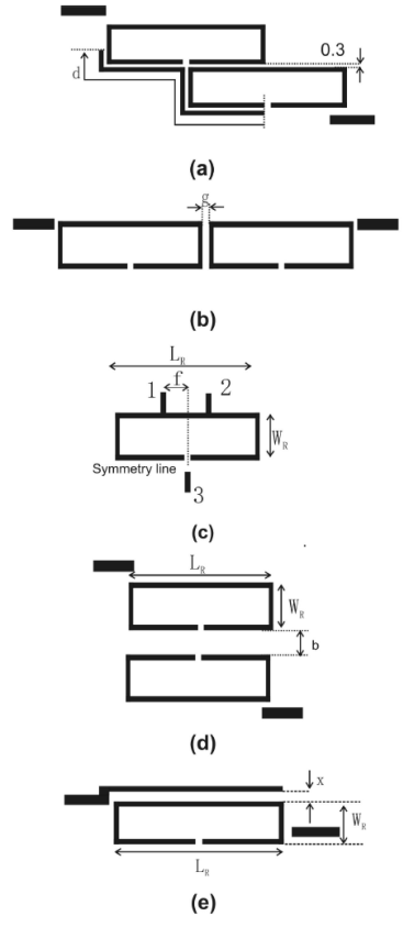
Figure 4 (a) Differential coupling of hairpin resonator using novel feed; (b) and (c) mutual coupling configuration; (d) differential external coupling; (e) mutual coupling; and (f) single ended external coupling. All dimensions are in millimeters.
To calculate the cross-coupling k a23, the structure in Fig. 4b is simulated in Ref. 16 for different gaps g and the results are depicted in Fig. 3. For our requirement, k a23 =0.014 hence g = 0.5 mm.
For the single-ended output external coupling (Fig. 4e), the required dimension for a Qa = 27, is x = 0.56 mm (Fig. 3). To adjust the position of the transmission zero, the second resonator’s width was slightly changed as seen in Fig. 5.
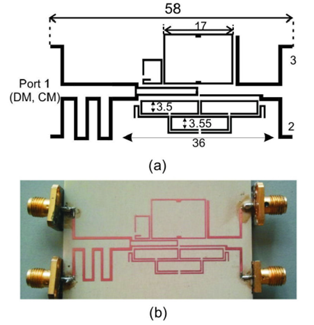
Figure 5 (a) Layout and (b) picture of diplexer with 3 pole hairpin filter and 2 pole ring filter. All dimensions are in mm.
For the second band we will use a 2 pole Chebyshev filter using ring resonators centered at fo = 2.06 GHz and FBW = 1.97%. A transmission zero is added at 2 GHz 19.
Firstly, we obtain the low pass prototype g values from20 for a 0.1 dB ripple, which are: go = 1, g 1 = 0.843, g 2 = 0.622 and g 3 = 1.355. Then, we calculate the mutual coupling between the ith and jth resonators (kij ) and external coupling (Q) using (2) and (3) respectively
 (2)
(2)
 (3)
(3)
Where gn is the nth g parameter for an nth order filter, gi is the g value of the ith resonator and gj for the jth resonator.
For our requirement, the external DM quality factor is Qd = 43 and the mutual coupling coefficient Is kc 12 = 0.027. To obtain the physical layout we simulate the structure in Fig. 6a in Ref. 16 for different values of La. The results are plotted in Fig. 7. For our requirement La = 0.4 mm. For this structure, the DM external coupling is 1250, therefore the DM is highly attenuated. Similarly, to calculate the mutual coupling, the structure in Fig. 6b was simulated In Ref. 16 for different notch widths (y) and the results are plotted in Fig. 7. Our final value is y = 2 mm. For the output coupling (Fig. 5b), the extracted external Q values plotted versus the length Lb are shown in Fig. 7. For our required Qb = 43 we get Lb = 12 mm. The final filter layout is shown in Fig. 5.
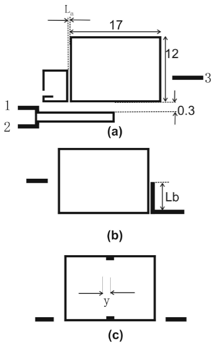
Figure 6 (a) External differential coupling of ring-resonator; (b) single-ended external coupling; and (c) mutual coupling. All dimensions are in mm.

The diplexer was fined tuned in Ref. 16 and then fabricated using photo-lithography (Fig. 5b). All the ports were measured with a 2 port Vector Network Analyzer and the unconnected ports were connected to a 50 Ω load. In order to obtain the final Differential and Common Mode responses, the experimental measurements were imported into 17 and an ideal 180° hybrid coupler was used to activate DM or CM respectively. The final experimental and simulated results are shown in Fig. 8.
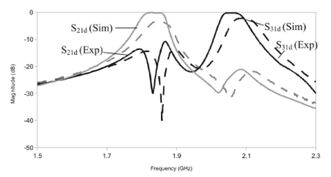
Figure 8 Experimental and simulated differential intersection losses of diplexer with differential input and single ended outputs.
For the first passband, the experimental center frequency is 1.85 GHz with an insertion loss (S21d) of 3.2 dB. For the second passband the experimental center frequency is 2.09 GHz with an insertion loss (S31d) of 2.5 dB. The experimental and simulated differential return losses (S11d) are better than 15 dB for both bands (Fig. 8). The CM insertion losses for the lower band filter (S21c) are better than 18 dB for the simulation and 20 dB for the experiment. For the second filter (S31c), the simulation insertion losses are greater than 13 dB and the experimental are greater than 16 dB.
It is important to note that the simulation results assume lossless conductors and dielectrics, resulting in much higher experimental losses. In addition, no filter tuning was performed during the experiment, for that reason, the differences between simulated and experimental results can also be attributed to manufacturing errors during the photolitograhy process, as well as material tolerances such as substrate thickness and permittivity.
4.- Diplexer with differential input, one single ended output and a differential output
As previously discussed, this topology is suitable for any type of output according to the chosen resonator. In this section we will describe the circuit having a differential antenna input, one differential output and one single ended output.
The 3 pole filter described in the previous section will be used at a center frequency fo = 1.77 GHz and having a differential output. For this, the output coupling was changed to the one shown in Fig. 4c as previously reported in Ref. 6. In this case, a differential signal will force a short circuit at the symmetry line. In order to extract the Qf = 27 parameter, the distance f was varied and simulated in Ref. 16. Then, from Fig. 3 the value of f is calculated as f = 1.0 mm. In this case LR = 14 mm and WR = 4 mm.
For the single ended output a 2-pole Chebyshev filter was designed at fo = 2.2 GHz with a fractional bandwidth FBW = 2.3%. The g values are described in Sec. 3. This leads to an external quality factor, Qc = 37 and a coupling factor kf12 = 0.03. In order to couple the circuit, the configuration shown in Fig. 4e was simulated at different x values. From Fig. 3, for the required Qc , x is 0.66 mm.
To obtain the mutual coupling value, the structure in Fig. 4d was simulated for different b values. The required b distance is extracted from Fig. 3 as b = 1.6 mm. Finally, for the differential input coupling, the structure of Fig. 2 is used and the gap value (p) is extracted from Fig. 3 as 0.6 mm. In this case LR = 12.2 mm and WR = 3.2.
The final filter layout and the fabricated prototype are shown in Fig. 10. To measure the filter a similar technique as in the previous sections was used. The simulation and experimental results are shown in Fig. 11 and 12.
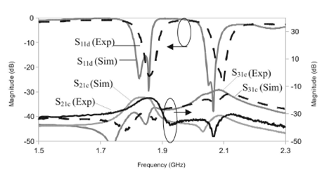
Figure 9 Experimental and simulated differential return losses of duplex with differential input and single ended outputs plus its common mode response.
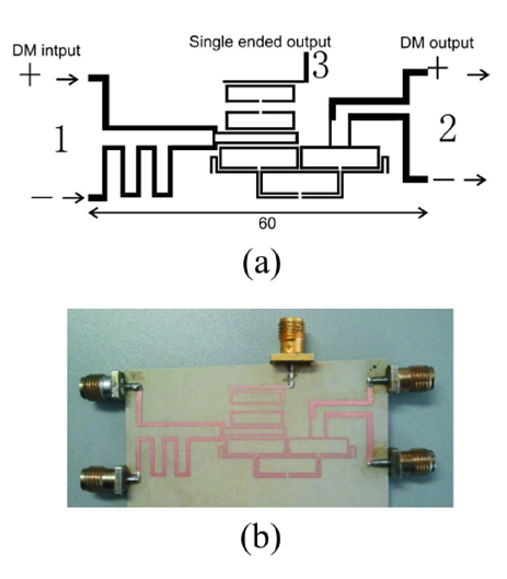
Figure 10 (a) Layout of diplexer with differential input and differential/single-ended outputs; (b) Fabricated diplexer. All dimensions are in mm.
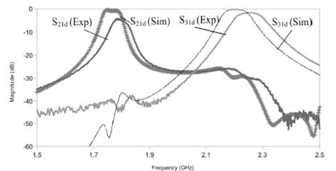
Figure 11 Experimental and simulated differential insertion losses of diplexer with differential input and differential/single ended outputs.
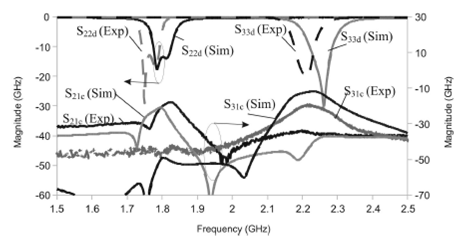
Figure 12 Experimental and simulated return losses of diplexer with differential input and differential/single-ended outputs, ant its common mode response.
For the first passband, the experimental center frequency is 1.78 GHz with an insertion loss (S21d) of 4 dB. For the second passband the experimental center frequency is 2.25 GHz with an insertion loss (S31d) of 1.6 dB. The experimental and simulated differential return losses at the filter output ports (S22d and S33d) are better than 14 dB for both bands (Fig. 12).
The CM insertion losses for the lower band filter (S21c) are better than 21 dB for the simulation and 18 dB for the experiment. For the second filter (S31c), the simulation has insertion losses greater than 12 dB and the experiment greater than 19 dB.
As in the previous circuit, perfect conductor and dielectric were assumed in the simulation, for that reason, insertion losses are much higher in the experiment. In addition, no tunning was performed during the experiment. The differences between simulated and experimental results are attributed to manufacturing and material tolerances.
5.- Conclusions
In this paper a novel differential mode diplexer topology has been presented. This structure allows complete design independence between both diplexer bands. In addition, this feed can be combined to provide single- ended or differential outputs while having a differential input. Two diplexers were shown, one has a differential input, and single-ended outputs; the other one has differential input, a single ended output and a differential output. All structures presented agreeable results between experiment and simulations

